Note: Descriptions are shown in the official language in which they were submitted.
CA 02314854 2003-12-17
1
OPTICAL COMMUNICATION SYSTEM OPTICALLY COMBINING BOTH
BASEBAND AND PASSBAND SIGNALS
Field Of The Invention
This invention relates to optical communication systems and, in particular,
to an optical communication system which optically combines baseband signals
and passband signals and transmits the combined signals over a common optical
fiber.
Background Of The Invention
An ever increasing communication need of today is to deliver multimedia
services such as voice, data, high speed Internet access, video conferencing,
video on demand, and broadcast television video to small businesses and
residences. Cost is the prominent issue for the deployment of such networks.
Among various technologies that are currently available and being deployed,
optical fiber extending to users -- Fiber to the Home (FTTH) -- is the
preferred
technology to meet present and future needs. Service providers are taking
fiber
as deep into their networks as their costs allow.
Two different optical fiber communication systems have evolved for
carrying information in digital formats to homes and businesses. One system
delivers information by a digitally modulated series of light pulses. These
are
referred to as baseband signals. A second system uses a plurality of frequency
separated carriers. Each carrier is modulated to transmit a digital
CA 02314854 2000-08-02
Chand 11-11-1-5-9 2
signal. These are passband signals. Each system has its own specialized
equipment, its own physical plant and its own standards.
Fig. 1A schematically illustrates a baseband system 10 comprising a
central office 11 providing optical fiber connections to a plurality of homes
12
and businesses 13. High power optical signals at single or multiple
wavelengths are transmitted over a plurality of access fibers 15A, 15B, 15C to
respective optical power splitters and/or wavelength demultiplexers 16A, 16B,
16C, and at each power splitter or demultiplexer, e.g., 16B, the high power
signal is divided into a plurality of lower power or separate wavelength
signals
and transmitted over a respective plurality of end user fibers 17A and 17B.
These signals are called downstream signals. The downstream signals are
typically a digitally modulated baseband series of light pulses centered in
the
1.3 - 1.6 wm wavelength band. Signals from the end users to the central
office, called upstream signals, are typically digitally modulated baseband
pulses in the same 1.3 -1.6 wavelength band but at different wavelength from
the downstream wavelength. They are transmitted in the reverse direction over
the same fibers. The upstream signals can be buffered and time division
multiplexed for burst transmission at the power splitters, e.g., 16B. Since
this
system does not employ any active electronic or photonic component between
the central office and the users, it is called a Passive Optical Network
(PON).
Fig. 1 B illustrates a simplified baseband modulation scheme. Typically,
a digital 1 is represented by a light pulse in the series. A digital 0, by the
absence of a pulse in a pulse position. Alternatively, the signal can be
inverted
with a pulse representing digital 0 and its absence representing 1.
Fig. 2A schematically illustrates a passband system 20 comprising a hub
21, and a plurality of fibers 22A, 22B, 22C connecting the hub to a respective
plurality of fiber nodes 23A, 23B and 23C. Each node is connected, as by a
plurality of fibers or coaxial cables 24A and 24B to a plurality of homes 12
and
businesses 13.
CA 02314854 2000-08-02
Chand 11-11-1-5-9 3
Fig. 2B illustrates the radio frequency spectrum of a typical digitally
modulated passband signal. The signal comprises a plurality of different radio
frequency (RF) carriers spaced apart in frequency (e.g. 6 MHz spacing in the
NTSC system). Each of the carriers is modulated among a plurality of states to
carry a higher order digital signal to encode plural bits for each modulation
state. The modulation can be amplitude modulation, frequency modulation,
phase modulation or a combination of them.
Digital passband signals are conventionally transmitted using two RF
carriers that are frequency locked but 90 degrees out of phase. The two
l0 carriers are said to be in quadrature. The two carriers are separately
amplitude
modulated (AM), and the modulated carriers are combined to form a single RF
output having both amplitude information corresponding to their vector sum and
phase information corresponding to their vector angle. The technique is known
as quadrature amplitude modulation or QAM.
Fig. 2C illustrates the simplest case of QAM which occurs when each of
the carriers has only two states (e.g. +V and -V). One carrier, is considered
the
reference carrier and is called the in-phase channel. Its amplitude is
represented along the horizontal axis of Fig. 2(C). The other carrier,
90° out of
phase, is called the quadrature charJnel. Its amplitude is represented along
the
vertical axis. As can be seen from the diagram, if each carrier has two states
(+V, -V), then there are four possible combined outputs, each of which can
represent two bits of information: (0,0), (0,1), (1,0), (1,1). This simple
modulation scheme is known as quadrature phase shift keying (QPSK).
Similar modulation schemes can be based on amplitude modulation of
the carriers among a larger number of states. For example if both carriers can
be modulated among four amplitudes, the combined output can represent 4 x 4
= 16 states, and the modulation is called 16 QAM modulation. Modulation
using 8 x 8 = 64 states is 64 QAM. With an increasing number of modulation
states, the required signal-to-noise ratio also increases.
CA 02314854 2003-12-17
4
In the past few years there has been an international effort from service
providers and system manufacturers to define common specifications aimed at
the extension of fiber all the way to homes and businesses to deliver existing
and
future services. These specifications are now part of International
Telecommunication Union (ITU) standard 6.983.1.
According to 6.983.1, all services are transported in baseband format in
both the upstream and downstream directions on a power splitter-based system.
In one variant of the network, a shared 1 55-Mbps baseband signal is
transported
downstream in the 1.5-pm band and the same bit rate is sent upstream in the
1.3-pm band on a single fiber. For low cost, a single transmitter in the
central
office and a single fiber can serve up to 32 users if the fiber is all the way
to the
user's premises. The number of users can even be greater if the receiver is at
the curb and electrical signals are distributed to multiple dwellings. The
6.983.1
specification calls for a minimum logical reach of at least 20 km and an
optical
power budget consistent with that reach. The specified downstream receiver
sensitivity at a bit error ratio of <10~° is -30 dBm for Class B
operation and
-33 dBm for Class C.
A downstream capacity of 155 Mbps shared among 32 end users is more
than adequate for interactive services such as voice, data, or interactive
video,
but can be quickly exhausted by multichannel broadcast video, especially if
high
definition TV (HDTV) is to be delivered. One approach to dealing with
broadcast
video delivery in 6.983.1 is to increase the downstream bandwidth from 155 to
622 Mbps. This approach is very expensive and complicates video channel
switching. Alternatively, video signals can be delivered on a separate fiber
using
a separate transmitter and a separate receiver. This approach is even more
expensive. Accordingly, there is a need for a new approach which improves the
performance and lowers the cost.
An optical communication system for gracefully combining both baseband
and passband signals on a common fiber is known.
CA 02314854 2003-12-17
In this system, the baseband and passband signals are electrically
combined, and the combined signal modulates an optical output signal at the
Central office. The optical signal can be sent over an optical fiber to a
remote
power splitter where it is passively power split among a plurality of fibers
to
5 respective end users. Within the power budgets of ITU-T 6.983.1, this
architecture can support the QPSK modulation format that satellite TV uses for
class B operation with a PIN diode receiver or class C operation with an APD
receiver: For terrestrial transmission of broadcast digital services, most
service
provider's, such as providers of cable TV, or wireless cable TV (MMDS
services),
use 64 QAM or higher order modulation. Compared to QPSK, delivery of 64
QAM modulated signal requires about 13 dB more signal to noise ratio in the
electrical domain which means 6.5 dBm more optical power at the receiver.
Alternatively, the receiver should be at least 6.5 dB more sensitive.
Experimental
data show that to deliver a 64 QAM modulated passband signal on top of a 155
Mbps baseband signal in class B of 6.983.1, an APD based receiver is required.
An APD is much more expensive than a PIN diode. The APD operation requires
a supply of typically more than 50V with much more complex voltage and
temperature stabilization circuitry as compared to a PIN diode that requires
less
than 5V and much simpler circuitry.
Telecommunication and Cable TV service providers would prefer to use 64
QAM or higher order modulation for broadcast digital services to make use of
their existing video infrastructure and to use the bandwidth efficiency of 64
QAM
that can deliver up to 6 bits per Hertz as opposed to a maximum of 2 bits per
Hertz by QPSK. To deliver 6.5 dBm more optical power for 64 QAM and to
remain within the power budgets of ITU-T 6.983.1 for the baseband signal,
there
is a need for a different architecture (system) that can combine baseband and
passband signals with an even higher level of performance.
CA 02314854 2000-08-02
Chand 11-11-1-5-9 6
Summary Of The Invention
This invention is a new communication system in which multichannel
broadcast digital services are distributed to each user with the broadcast
services signal riding in the passband above a digital baseband signal. The
system can deliver more than 1 Gbps additional bandwidth to each subscriber.
The passband bandwidth will accommodate growth in downstream services
including video on demand, higher speed web downloads including improved
streaming audio and video, HDTV, interactive video, and personalized video.
The invention requires only a single fiber path and a single optical receiver
for
each user or group of users. A single fiber, single optical receiver system is
much less expensive than two systems, one transmitting baseband and the
other passband. A single receiver is greatly cost beneficial to achieving
economical fiber to the home.
Although the result of the invention is to add digital video and other
bandwidth demanding services on the system described in 6983.1, it can also
be used in other architectures where specifications or requirements differ
from
6983.1. For example, upstream or downstream data rate and optical
wavelengths and the required receiver sensitivity and bit error rates may vary
according to the specific application. The invention can also be used in point
to point transmission of baseband and passband signals on a single fiber and
receiver. Furthermore, the optical receiver or ONT does not have to be at the
customer premises. It can be outside on the curb. From the curb, the
baseband and passband services can be delivered to subscribers sharing that
ONT on twisted copper wires or coaxial cables, in an architecture popularly
known as Fiber to the Curb (FTTC). For twisted copper wires, the services can
be delivered using any of the conventional digital subscriber line techniques.
For coaxial lines, hybrid fiber-coaxial (HFC) technology is used.
In an exemplary embodiment, an optical communication system
comprises a first optical transmitter for generating an optical baseband
signal,
t
CA 02314854 2000-08-02
Chand 11-11-1-5-9 7
a second optical transmitter for generating an optical passband signal, an
optical power coupler for combining the signals, a length of optical
transmission
fiber for transmitting the combined optical signal, and one or more receivers
optically coupled to the fiber. In an advantageous system, an optical power
splitter is optically coupled to the transmission fiber for power splitting
the
transmitted signal among a plurality of end-user fibers, and, for each user or
group of users, an optical receiver is coupled to the user fiber.
Brief Description Of The Drawin4s
The advantages, nature and various additional features of the invention
l0 will appear more fully upon consideration of the illustrative embodiments
described in connection with the accompanying drawings. In the drawings:
Figs. 1A and 1B illustrate features of a typical baseband communication
system;
Figs. 2A, 2B and 2C illustrate features of a typical passband
communication system;
Fig. 3 is a schematic block diagram of an exemplary optical
communication system combining both baseband and passband signals;
Fig. 4 is a schematic diagram of an optical transceiver for the system of
Fig. 3;
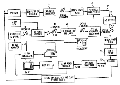
Fig. 5 is a diagram of a test system combining both baseband and
passband signals; and
Figs. 6-9 are graphical illustrations showing the results of tests using the
system of Fig. 5.
It is to be understood that these drawings are for purposes of illustrating
the concepts of the invention and, except for the graphs, are not to scale.
CA 02314854 2003-12-17
8
Detailed Description
Figs. 1 and 2, which relate to conventional baseband and conventional
passband systems were described in the Background of the Invention.
Fig. 3 is a schematic block diagram of an optical communication system
30 for combining both baseband signals and passband signals on one or more
common optical transmission fibers 32. In essence, the system 30 comprises a
first optical transmitter 40 responsive to an input electrical baseband signal
from
a baseband source 28 and a second optical transmitter 41 responsive to an
input
electrical passband signal from a passband source 29. Transmitter 40 can be a
digital transmitter (e.g. directly modulated digital laser) digital laser, and
transmitter 41 can be an analog transmitter (e.g. an analog laser or an
externally
modulated digital laser). Both transmitters 40 and 41 can be semiconductor
lasers. The transmitters 40, 41 separately generate optical signals containing
the
information of their respective input signals. The optical signals are then
optically
combined in an optical combiner such as an optical power coupler 42, and the
combined optical signal is transmitted to one or more optical receivers 35. At
least one optical receiver 35 can detect and demodulate both the baseband
signal and the passband signal. It is contemplated that the transmitters 40,
41
will be located at a central office. It is also possible that the electrical
to optical
conversion of the passband signal may occur deeper in the network, presenting
an optical passband signal at the central office.
In the preferred arrangement shown in Fig. 3 the passband signal
comprises broadcast digital signals that will be virtually the same for all
users
whereas the baseband signal is dedicated to a particular group of users.
Accordingly, it may be advantageous to amplify the optical passband signal in
an
erbium doped fiber amplifier (EDFA) 43 and apply the amplified output to an
optical power splitter 44. This provides plural optical passband signals that
can
be combined with other dedicated baseband signals for other groups of users
(not shown).
CA 02314854 2000-08-02
Chand 11-11-1-5-9 9
In one embodiment, the baseband signal is a digitally modulated time
division multiplexed (TDM) 155 Mbps baseband signal conforming to the power
budgets and other specifications of the ITU industry standard 6983.1. The
passband signal is a quadrature phase-shift keying frequency division
multiplexed (FDM) signal carrying greater than 1 Gbps of information. The
baseband and passband signals are converted by transmitter lasers 40 and 41
into two different wavelengths in the 1.5 ~,m band such that the optical
interaction between the two wavelengths does not cause any distortion of the
baseband and passband signals which are combined in the optical domain.
Although the preferred embodiment of this invention uses a single optical
receiver for both baseband and passband signals for low cost, a variant of
this
invention may use an integrated optical module at the receiver to separate the
passband signal for detection by a separate O/E receiver or for delivery to
another location with a separate fiber.
An important advantage of this system is that the optical transmitters 40
and 41 can be separately optimized for their respective signals. Such
optimization eliminates a 1 to 2 dB transmitter-related optical power penalty
that would be incurred if a single transmitter were used, and it improves
system
performance. For example, the optical path for the passband signal can
include an additional erbium doped fiber amplifier 44 to optimize passband
transmission.
Fig. 4 schematically illustrates an advantageous optical transceiving
arrangement 35 for end-users. The arrangement receives the transmitted
combined optical signal from a fiber 34 through a MUX 50. The combined
signal is applied to a receiving element 51, such as a PIN diode, and the
resulting combined electrical signal is fed into a preamplifier 52. The
preamplified combined electrical signal is then split by diplexer 53 into its
baseband portion and its passband portion.
CA 02314854 2000-08-02
Chand 11-11-1-5-9 10
To permit two-way communication with the end user, the transceiver 35
may advantageously include a transmitter laser 54 for receiving electrical
signals from the users and generating an optical return signal at wavelength
different from the optical input signal. This return signal is presented to
the
multiplexer 50 and sent back toward the central office by fiber 34. The input
downstream signals are preferably at two spaced apart wavelengths in the
1.48-1.60 p,m range and the output upstream signal is preferably at 1.3 ~,m.
The invention may now be better understood by consideration of the
following specific examples and tests. In the examples and tests, which are
l0 intended for those skilled in the art, the acronyms used are expanded when
they are first used and in the definitions section at the end of this
specification.
The following examples are provided for the purpose of illustration only.
The examples should not be construed as limiting the invention.
Example 1
This example is to demonstrate this invention's feasibility. The
experimental detail combined with the description above shows advantages of
various possible components and methods.
Fig. 5 schematically illustrates the test apparatus wherein an electrical
baseband modulation signal applied to a DFB laser transmitter 40 generates
an optical baseband signal. An electrical 64 QAM passband signal derived
from a MMDS signal is converted to an optical passband signal in a second
DFB laser 41, and the baseband and passband optical signals are combined in
a 2x2 optical power combiner 42, transmitted over a common fiber 32 to a
power splitter 33. An arm 34 of the splitter transmits a portion of the
received
optical signal to an end-user receiver 35 including a diplexer 53. The
receiver
34 was a Lucent Technologies 1319 OIE receiver. The receiver comprises a
PIN detector and a transimpedance amplifier (TIA). A diplexer 53 is used to
separate the baseband and passband signals at the output of the receiver.
CA 02314854 2000-08-02
Chand 11-11-1-5-9 11
Electrical circuitry pertinent to the particular passband signal used and to
the
tests conducted (but not to the actual systems using the invention) will be
described in connection with these tests.
We have used a 64-QAM MMDS video signal for the passband signal.
The signal comprises 31 carriers with 4 empty slots in 222-408 MHz. Each
carrier is 6 MHz wide and carries 5.063 M symbolsls. At one of the empty slots
at 279 MHz, we inserted a 6 MHz wide 64-QAM test carrier for bit error rate
and constellation studies from a Broadcom modulator. The power level of the
test carrier was adjusted to the level of the MMDS carriers. The DAVIC
scheme was used for forward error correction (FEC) as offered by the
Broadcom modulator 60. For the passband signal, we used both a directly
modulated DFB digital laser transmitter and a commercially available
transmitter from Harmonics Lightwave that is optimized for analog signals.
The outputs of the receiver 35 are shown in Figs. 6(a), 6(b) and 6(c).
Fig. 6(a) shows the composite signal at the output of the receiver. This
composite includes both the baseband and the passband signals with a notable
separation between them.
Fig. 6(b) shows the high frequency output of the diplexer comprising the
MMDS digital video carriers in 222-408 MHz. This constitutes the passband
2o signal.
Fig. 6(c) shows the low frequency output of the diplexer constituting the
155 Mbps baseband signal. The diplexer separated the baseband and
passband signals with negligible insertion loss for either signal.
Fig. 7 compares the system performance of an analog transmittter
optimized for analog signals with a digital transmitter for the passband
signal.
The analog transmitter was obtained as a commercial product from Harmonic
Lightwave. The circuit of this transmitter had been designed for optimum
analog video modulation. The digital transmitter has a DFB laser on a laser
CA 02314854 2000-08-02
Chand 11-11-1-5-9 12
test fixture. Fig. 7 plots the bit error rate of the received signal versus
the
received optical power. The measurements were taken on the 279 MHz test
carrier with all MMDS carriers present but without the baseband signal
present.
Data are shown for both digital and analog transmitters and before and after
forward error correction. The forward error correction in the DAVIC scheme
provides about 4 dB optical coding gain for a bit error rate of
10-'°. The coding gain decreases with increasing bit error rate. The
data shows
that the analog transmitter gives a 2-dB optical power improvement in system
performance as compared to the digital transmitter.
to Qualitatively, no impairment was observed in the picture quality or sound
quality of the 285 MHz channels on TV for a test channel bit error rate of
less
than 5 x 10⁻³ before forward error correction. This corresponds to -26.5 dBm
passband optical power at the receiver. After FEC, this corresponds to about
10~'° BER. It is believed that a system built for a 10-s BER before FEC
will
result in an essentially error free signal after FEC. This requires about -
24.5
dBm optical signal at the receiver in the absence of a baseband signal.
Figs. 8(a) - 8(c) plot the logarithmic error probability of the passband in
the presence of respectively different baseband optical power levels. Fig.
8(a)
is measured with -28 dBm of baseband optical power, Fig. 8(b) with -25 dBm
and Fig. 8(c) with -22 dBm optical powers. The optical power penalty on
passband due to the presence of baseband varies with the baseband power.
The optical power penalty is 0.2 dB, 0.6 dB and 0.75 dBm for baseband powers
of -28 dBm, -25 dBm and -22 dBm, respectively.
Fig. 9 shows the logarithmic error probability of the baseband with and
without the presence of a passband signal at -24 dBm and -25 dBm optical
power. Based on these measurements and other measurements at high
passband optical power, it is believed that the presence of a passband signal
at less than -11 dBm optical power adds negligible noise in the baseband
region. The baseband power penalty is less than 0.5 dB.
CA 02314854 2000-08-02
Chand 11-11-1-5-9 13
As the baseband optical power increases beyond -22 dBm, the noise
due to baseband harmonics increases in the RF range of the passband. This
increases the power penalty on passband as shown in Figs. 8(a)-8(c). Thus
baseband harmonics should be minimized by filtering the baseband signal and
biasing the baseband laser in a linear region. This may reduce the extinction
ratio in the baseband below the FSAN required 10 dB. Nonetheless, the
system can operate at less than -22 dBm for either type of signal.
These tests show that a digitally modulated passband signal can be
delivered over the same optical fiber along with a baseband signal. This
l0 system can use most existing transmission equipment and baseband
transmission power budgets (e.g. ITU-T 6983.1 ). Approximately 1-5 Gbps
transmission rates can be achieved compatible with existing components. This
additional bandwidth can be used for broadcast and switched video and for
other bandwidth demanding services. It can also be used to provide a
dedicated channel of desired bandwidth to any subscriber. The proposed
technique also provides a graceful upgrade of currently installed passive
optical networks without incurring significant additional costs or power
penalty.
If some subscribers want to receive baseband data only and no video or any
other passband services, the system is compatible with baseband only ONU
with negligible power penalty.
It will be clear to those skilled in the art that many modifications and
variations may be made to the embodiments as described without substantially
departing from the spirit and scope of the present invention. It is intended
that
all such modifications and variations be included herein within the scope of
the
present invention, as is set forth in the appended claims.
CA 02314854 2003-12-17
14
DEFINITIONS
Acronym Meaning
APD avalanche photodetector
BER bit rate error
DAVIC digital audio visual council
DSS digital satellite service
EDFA erbium doped fiber amplifier
FDM frequency division multiplexing
FEC forward error correction
FTTC fiber to the curb
FTTH fiber to the home
Gbps gigabits per second
HDTV high definition television
ITU International Telecommunications Union
LNB low noise block
Mbps megabits per second
MMDS multichannel multipoint distribution system
M-QAM quadrature amplitude modulation, where M is the
number of
modulation states
OIE optical-to-electrical
OMD optical modulation depth
OMI optical modulation index
ONT optical receiver
ONU optical network unit
CA 02314854 2003-12-17
PON passive optical network
QAM quadrature amplitude modulation
QPSK quadrature phase shift keying
RF radio frequency
R-S coding Reed-Solomon coding
SNR signal-to-noise ratio
STB set top boxes
TDM time division multiplexing