Note: Descriptions are shown in the official language in which they were submitted.
CA 02314879 2000-06-19
. ' - 1 -
SPECIFICATION
DIGITAL DEMODULATOR
TECHNICAL FIELD
The present invention relates to a digital demodulator used
with a digital broadcasting receiver for receiving BS digital
broadcasting programs, and more particularly to a digital
demodulator used with a digital broadcasting receiver for receiving
time-multiplexed waves which were digitally modulated by a plurality
of modulation methods having different necessary C/ N(a ratio of
carrier power to noise power) values.
BACKGROUND ART
In a BS digital broadcasting method, a hierarchical
transmission method of repetitively transmitting, one frame after
another, time-multiplexed digital main signals which were modulated
by a plurality of modulation methods having different necessary C/N
values, such as 8PSK modulated waves, QPSK modulated waves, and
BPSK modulated waves, in addition to burst symbol signals inserted
in the main signals and capable of being received at a low C/N value.
The burst symbol signal is a signal which was BPSK modulated by a
known PN code.
In such a hierarchical transmission method, a frame sync
pattern and a superframe identification signal have predetermined
CA 02314879 2000-06-19
- 2 -
patterns which were BPSK modulated. A digital demodulator of a
digital broadcasting receiver performs absolute phasing which makes
the reception phase be coincident with the transmission phase, in
order to decode the demodulated baseband signal by a decoder or to
perform other operations. In the hierarchical transmission method,
a frame sync signal, a TMCC signal for transmission and multiplexing
configuration control to be described later and a burst symbol signal
are BPSK demodulated, and the absolute phasing is performed in
accordance with the reception phase of the received frame sync
pattern (absolute phase reception, inverse phase reception).
However, a necessary circuit area of an integrated digital
demodulator becomes large because of the presence of an absolute
phasing circuit.
An object of the invention is to provide a digital demodulator
which does not require an absolute phasing circuit.
DISCLOSURE OF THE INVENTION
The invention provides a digital demodulator for a digital
broadcasting receiver for receiving digital modulated waves
multiplexed in time axis by a plurality of modulation methods,
comprising:
inverter means for selectively inverting demodulated baseband
signals in accordance with a BPSK signal having a known pattern
prepared in advance; and
CA 02314879 2000-06-19
- 3 -
carrier reproduction phase error detector means provided with
a phase error table having a phase converging point as an absolute
phase, the carrier reproduction phase error detector means
outputting a phase error signal corresponding to a phase difference
between a phase obtained from a signal point of the demodulated
baseband signals output from the inverter means and a phase of the
phase converging point,
wherein carrier reproduction is executed by controlling a
frequency of a reproduction carrier so as to make the phase of the
signal point become coincident with the phase converging point.
According to the digital demodulator of this invention, the
demodulated baseband signals are selectively inverted in accordance
with the phase of the BPSK signal having the known pattern prepared
in advance. Therefore, the reference point of the demodulated
baseband signals selectively inverted takes an absolute phase. The
reference point of the demodulated baseband signals not inverted
takes also the absolute phase. The carrier reproduction phase error
detector means refers to the phase error table, and outputs a phase
error signal corresponding to a phase difference between the phase
obtained from a signal point of the demodulated baseband signals
selectively inverted and the phase of the phase converging point of
the absolute phase. The carrier reproduction is executed by
controlling the frequency of the reproduction carrier so as to make
the phase of the signal point become coincident with the phase
CA 02314879 2000-06-19
- 4 -
converging point. The phase point of the reception signal is therefore
converged to the absolute phase and the reception signal is subjected
to the absolute phasing. An absolute phasing circuit is therefore
unnecessary.
The digital demodulator of this invention further comprises the
carrier filter of a low-pass filter, the carrier filter being input with the
phase error signal from the carrier reproduction phase error detector
means and stopping a filtering operation during a TMCC section, and
a BPSK signal section, a QPSK signal section and an 8PSK signal
section of main signals, and the carrier reproduction being executed
in accordance with an output of the carrier filter.
The digital demodulator of this invention is provided with the
carrier filter of a low-pass filter whose filtering operation stops during
the TMCC section, and the BPSK signal section, a QPSK signal
section and an 8PSK signal section of the main signals. Although
the phases of the demodulated baseband signals during the BPSK
signal section, QPSK signal section and 8PSK signal section of the
main signals are compared with the absolute phase, the filtering
operation of the carrier filter stops during these signal sections and
any practical problem will not occur.
BRIEF DESCRIPTION OF THE DRAWINGS
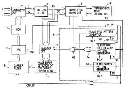
Fig. 1 is a block diagram showing the structure of a digital
modulator according to an embodiment of the invention.
CA 02314879 2000-06-19
- 5 -
Figs. 2(A) - 2(G) are a diagram showing the structure of a frame
used by the digital modulator of the embodiment and waveforms of
signals Rs, A1, AO, As, Bs and SF.
Fig. 3 is a block diagram showing. the structure of an arithmetic
circuit and a numerical control oscillator of the digital demodulator of
the embodiment.
Figs. 4(A) and 4(B) are a diagram illustrating a superframe
identification pattern in a frame of a signal supplied to the digital
demodulator of the embodiment.
Figs. 5(A) and 5(B) are a phase error table used by the digital
demodulator of the embodiment.
EMBODIMENT OF THE INVENTION
An embodiment of a digital demodulator according to the
invention will be described.
Fig. 1 is a block diagram showing the structure of the digital
demodulator of the embodiment.
Prior to describing the digital demodulator according to the
embodiment of the invention, the structure of a frame used by the
hierarchical transmission system will be described. Fig. 2(a) is a
diagram showing an example of the frame structure used by the
hierarchical transmission system. One frame is constituted of one
header of 192 symbols and a plurality of pairs of 203 symbols and 4
symbols, totaling in 39936 symbols.
CA 02314879 2000-06-19
- 6 -
More specifically, one frame is constituted of: a frame sync
pattern (BPSK) of 32 symbols (of 32 symbols, front 20 symbols are
used); a transmission and multiplexing configuration control (TMCC)
pattern (BPSK) of 128 symbols for transmission multiplexing
configuration identification; a superframe identification information
pattern of 32 symbols (of 32 symbols, front 20 symbols are used); a
main signal (TC8PSK) of 203 symbols and a burst symbol signal of 4
symbols (indicated by BS in Fig. 2(a)) to be BPSK modulated by a
pseudo-random signal set per each frame period; a main signal
(TC8PSK) of 203 symbols and a burst symbol signal of 4 symbols;,,,;
a main signal (QPSK) of 203 symbols and a burst symbol signal of 4
symbols; and a main signal (BPSK) of 203 symbols and a burst
symbol signal of 4 symbols, respectively arranged in this order. 8
frames are called a superframe and the superframe identification
information pattern is used for identifying the superframe.
Referring back to Fig. 1, the digital demodulator according to
the embodiment of the invention will be described. The digital
modulator of the embodiment has an arithmetic circuit 1, a
numerical control oscillator 2, a roll-off filer 3 made of a digital filter
having the raised cosine characteristics, a frame sync timing circuit 4,
a transmission mode judging circuit 5, an inversion command signal
generator circuit 6 for generating an inversion command signal of "0"
or " 1" in accordance with a BPSK signal having a known pattern; an
inverter circuit 7 for inverting the demodulated baseband signals ID
CA 02314879 2000-06-19
- 7 -
and QD at the same time when necessary, in response to the
inversion command signal output from the inversion command signal
generator circuit 6; a carrier reproduction phase error detector circuit
8 having a carrier reproduction phase error table with a phase
converging point at the absolute phase; a carrier filter 9 of a low-pass
digital filter, an AFC circuit 10, and an AND circuit 11 for controlling
the operation of the carrier filter 9.
As shown in Fig. 3, the numerical control oscillator 2 has a
sine table 23 for outputting sine data 23a and 23b of opposite
polarities and a cosine table 24 for outputting cosine data 24a and
24b. In accordance with the output from the AFC circuit 10, the
numerical control oscillator 2 outputs the sine data 23a and 23b and
cosine data 24a and 24b of opposite polarities, to output sine and
cosine signals of opposite polarities which substantially form
reproduction carriers in cooperation with the AFC circuit 10.
The arithmetic circuit 1 has as shown in Fig. 3: a multiplier la
for multiplying a quasi-sync detected I axis baseband signal i by the
sine data 23a; a multiplier lb for multiplying the baseband signal i
by the cosine data 24a; a multiplier ld for multiplying a quasi-sync
detected Q axis baseband signal q by the opposite polarity sine data
23b; a multiplier le for multiplying the baseband signal q by the
cosine data 24b; an adder lc for adding outputs of the multipliers lb
and ld and outputting the addition result as a baseband signal I; and
an adder lf for adding outputs of the multipliers la and le and
CA 02314879 2000-06-19
- 8 -
outputting the addition result as a baseband signal Q. The
arithmetic circuit 1 therefore tunes the frequencies of the baseband
signals i and q and outputs the frequency tuned baseband signals I
and Q to the roll-off filter 3.
Upon reception of baseband signals ID and QD output from the
roll-off filter 3, the frame sync timing circuit 4 outputs a TMCC
pattern to the transmission mode judging circuit 5. In accordance
with the decoded result of the TMCC pattern, the transmission mode
judging circuit 5 supplies the frame sync timing circuit 4 with a 2-bit
transmission mode signal representing a high hierarchical 8PSK
signal (demodulated from the 8PSK modulated signal); a low
hierarchical QPSK signal (demodulated from the QPSK modulated
signal); and a low hierarchical BPSK signal (demodulated from the
BPSK modulated signal).
The frame sync timing circuit 4 receives the baseband signals
ID and QD to detect a sync pattern and output a frame sync signal
FSYNC to the AFC circuit 10 which -executes an AFC operation for
each frame, and also receives the transmission mode signal from the
transmission mode judging circuit 5 to output: a signal Rs shown in
Fig. 2(B) which synchronizes with the start of the frame sync pattern;
a signal Al shown in Fig. 2(C) which takes a high level during the
BPSK signal section; a signal A0 shown in Fig. 2(D) which takes the
high level during a frame sync pattern section, a superframe
identification pattern section, a burst symbol signal section and a
CA 02314879 2000-06-19
- 9 QPSK signal section, a signal As shown in Fig. 2(E) which takes the
high level during the frame sync pattern section, a signal Bs shown in
Fig. 2(F) which takes the high level during the burst symbol signal
section, and a signal SF shown in Fig. 2(G) which takes the high level
during the superframe identification pattern section.
Next, the superframe identification pattern will be described.
Fig. 4(A) is a diagram showing the superframe identification pattern.
W, represents the frame sync pattern, and takes the same pattern for
all frames. In Figs. 4(A) and 4(B), patterns W2 and W3 represent the
superframe identification patterns including the frame sync pattern
and superframe identification pattern extracted from each frame.
The pattern W2 is used as the superframe identification pattern for
the first frame, and the pattern W3 is used as the superframe
identification pattern for all seven other frames from the second to
eighth frames. The pattern W3 is an inverse pattern of the pattern
W2.
The frame sync timing circuit 4 outputs a superframe
identification pattern identification signal which identifies the
superframe identification pattern taking the low level during the
section of the superframe identification pattern W2 of the start frame
shown in Fig. 4(B) and the high level during the section of the
superframe identification pattern W3 of the following seven frames.
The inversion command signal generator circuit 6 has a frame
sync pattern generator circuit 61, a superframe identification pattern
CA 02314879 2000-06-19
- 10 -
generator circuit 62, a burst symbol pattern generator circuit 63, an
exclusive OR circuit 64, and an OR gate circuit 65 which outputs the
inversion command signal.
The frame sync pattern generator circuit 61 is reset by the
signal Rs and receives as the enable signal the signal As, i.e., the
signal output during the frame sync pattern section. Synchronously
with a bit clock signal, the frame sync pattern generator circuit 61
sequentially outputs via the OR gate circuit 65 the signal constituting
the frame sync pattern as the inversion command signal. For
example, the inversion command signal takes a bit "1" to enable the
inversion command.
The superframe identification pattern generator circuit 62 is
reset by the signal Rs and receives as the enable signal the signal SF,
i.e., the signal output during the superframe identification pattern
section. Synchronously with the bit clock signal, the superframe
sync pattern generator circuit 62 sequentially outputs the superframe
identification pattern W2 constituting the start frame to the exclusive
OR circuit 64. The pattern W2 is subjected to the exclusive OR
operation with the superframe identification pattern identification
signal output from the frame sync timing circuit 4 and the result is
supplied to the OR gate circuit 65. In accordance with the
superframe identification pattern identification signal, the exclusive
OR circuit 64 outputs the superframe identification pattern W2 for
the start frame, and the pattern W3 inverted from the pattern W2 for
CA 02314879 2000-06-19
- 11 -
the following seven frames. Therefore, the exclusive OR circuit 64
outputs the superframe identification pattern signals W2, W3, W3, W3,
W3, W3, W3, and Wa shown in Fig. 4(A) for the frames from the start to
eighth frames via the OR gate circuit 65 as the inversion command
signals. For example, the inversion command signal takes a bit " 1"
to enable the inversion command.
The burst symbol pattern generator circuit 63 is reset by the
signal Rs and receives as the enable signal the signal Bs, i.e., the
signal output during the burst symbol pattern section.
Synchronously with the bit clock signal, the burst symbol generator
circuit 63 sequentially outputs via the OR gate circuit 65 the burst
symbol signal as the inversion command signal. The burst symbol
pattern generator circuit 63 therefore outputs the burst symbol signal
as the inversion command signal. For example, the inversion
command signal takes a bit " 1" to enable the inversion command.
Therefore, the inversion command signal generator circuit 6
outputs the frame sync pattern signal as the inversion command
signal " 1" during the frame sync pattern section, outputs as the
inversion command signal the signal " 1" of the signal shown in Fig.
4(A) corresponding to each frame during the superframe identification
pattern section, and outputs as the inversion command signal the
burst symbol signal " 1" during the burst symbol pattern section.
In accordance with the inversion command signal output from
the inversion command signal generator circuit 6, the inverter circuit
CA 02314879 2000-06-19
- 12 -
7 inverts the baseband signals ID and QD output from the roll-off
filer 3 at the same time when necessary. More specifically, when the
inversion command signal takes the low level, the baseband signals
ID and QD are directly sent to the carrier reproduction phase error
detector circuit 8, whereas when the inversion command signal takes
the high level, the baseband signals ID and QD are inverted at the
same time and sent to the carrier reproduction phase error detector
circuit 8.
Upon reception of the baseband signals ID and QD via the
inverter circuit 7, the carrier reproduction phase error detector circuit
8 detects a phase error between the phase calculated from the signal
point of the baseband signals ID and QD and the absolute phase to
thereby output a phase error voltage corresponding to the phase
error.
More specifically, the carrier reproduction phase error detector
circuit 8 has a carrier reproduction phase error table shown in Fig.
5(A) with the phase converging point (0 (2n) radian) of the absolute
phase. The phase is obtained from the signal point of the baseband
signals ID and QD supplied from the inverter circuit 7, and the phase
error voltage corresponding to the phase is obtained from the carrier
reproduction phase error table and supplied to the carrier filter 9.
The reference point of the phase of the signal point of the
baseband signals ID and QD output from the roll-off filter is either 0
(2n) radian or n radian. However, if the signal output from the
CA 02314879 2000-06-19
- 13 -
inversion command signal generator circuit 6 as the inversion
command signal during the frame sync pattern section, superframe
identification pattern section or burst symbol section takes the high
level, the baseband signals ID and QD output from the roll-off filter 3
are inverted at the same time and the reference point of the phase of
the signal point of the inverted baseband signals ID and QD is 0(2n)
radian. Conversely, if the signal output from the inversion command
signal generator circuit 6 as the inversion command signal during the
frame sync pattern section, superframe identification pattern section
or burst symbol section takes the low level, the baseband signals ID
and QD output from, the roll-off filter 3 are not inverted but are
directly output from the inverter circuit 7 and the reference point of
the phase of the signal point of the inverted baseband signals ID and
QD is 0 (2n) radian.
Therefore, the reference point of the phase obtained from the
signal point of the baseband signals ID and QD input to the carrier
reproduction phase error detector circuit is 0(2n) radian, so that the
phase error can be detected from the carrier reproduction phase error
table shown in Figs. 5(A) and 5(B).
If the phase obtained from the signal point of the baseband
signals ID and QD input from the inverter circuit 7 has a phase in
the increase direction from n radian or larger to 0(2n) radian, a
negative phase error voltage shown in Figs. 5(A) and 5(B) is output,
whereas if the phase has a phase in the decrease direction from
CA 02314879 2000-06-19
- 14 -
smaller than n radian to 0(2n) radian, a positive phase error voltage
shown in Figs. 5(A) and 5(B) is output. This phase error voltage is
supplied to the AFC circuit 10. Under the control of the AFC circuit
10, the phase obtained from the signal point is converged to 0(2n) as
shown in Fig. 5(B). In this case, the phase error voltage takes a plus
direction maximum value or minus direction maximum value at the
phase of n radian.
The phase error voltage corresponding to the phase obtained
from the signal point of the baseband signals ID and QD and output
from the carrier reproduction phase error detector circuit 8 is
supplied to the carrier filer 9 of the digital low-pass filter and
smoothed. In the case of the minus direction, the signal obtained
through the logical AND of the signals A I. and A0 by the AND circuit
11 is supplied as a carrier filter control signal (CRFLGP), and the
carrier filer 9 executes a filtering operation only during the frame
sync pattern section, superframe identification pattern section and
burst symbol signal section. During the BPSK signal section, QPSK
signal section and 8PSK signal section of the main signals, the low
level signal is output from the AND circuit 11 to stop the filtering
operation of the carrier filter 9. Therefore, the output of the carrier
filter 9 is maintained at the output immediately before the filtering
operation is stopped. The output of the carrier filer 9 is supplied as
a tuning voltage to the AFC circuit 10.
As the baseband signals of the main signals during the BPSK
CA 02314879 2000-06-19
- 15 -
signal section, QPSK signal section and 8PSK signal section are
supplied to the carrier reproduction phase error detector circuit 8,
the phase error voltage is detected from the carrier reproduction
phase error table (refer to Figs. 5(A) and 5(B)) having the reference
point of 0(2n) radian. However, in this case, the carrier filter 9 is
disabled so that any practical problem will not occur.
The operation of the digital demodulator constructed as above
according to the embodiment of the invention will be described.
In a BS digital broadcasting receiver, generally, a desired signal
in a designated channel is scanned by the AFC circuit 10 to capture
the carrier. In the digital demodulator according to the embodiment
of the invention, upon reception of a desired signal, the baseband
signals i and q orthogonally demodulated by the quasi-detection
method are supplied to the arithmetic circuit 1 which calculates the
baseband signals i and q by using the output data from the
numerical control oscillator 2 and converts the signals i and q into
the baseband signals I and Q.
The baseband signals I and Q are supplied to the roll-off filter 3
which outputs the baseband signals ID and QD. The baseband
signals ID and QD are supplied via the inverter circuit 7 to the carrier
reproduction phase error detector circuit 8 which obtains the carrier
reproduction phase error voltage in accordance with the phase
corresponding to the signal point of the baseband signals ID and QD
supplied via the inverter circuit 7. The phase error voltage is
CA 02314879 2000-06-19
- 16 -
smoothed by the carrier filter 9 and supplied as the tuning voltage to
the AFC circuit 10. An output of the AFC circuit 10 is supplied to
the numerical control oscillator 2 to reproduce the carrier by
controlling the carrier frequency to make the phase error voltage
become zero.
The baseband signals ID and QD are also supplied to the frame
sync timing circuit 4 which detects the frame sync pattern to capture
the frame sync and establish the frame timing. The time sequential
positions of the frame sync pattern, TMCC pattern, superframe
identification pattern and burst symbol signals are therefore
identified. The TMCC pattern is sent to the transmission mode
judging circuit 5 and decoded. Upon reception of the transmission
mode signal output from the transmission mode judging circuit 5, the
frame sync timing circuit 4 outputs the signals Rs, Al, AO, As, Bs
and SF.
Upon reception of the signals Rs, As, Bs and SF and
superframe identification pattern identification signal sent from the
frame sync timing circuit 4, the inversion command signal generator
circuit 6 identifies the reception phase points at respective timings
from the phases and timings of the frame sync pattern signal,
superframe identification pattern signal and burst symbol signal, and
outputs the inversion command signals having the high or low level
to be determined from the reception phase point, to the inverter
circuit 7.
CA 02314879 2000-06-19
- 17 -
Upon reception of the inversion command signal, the inversion
circuit 7 supplies the baseband signals ID and QD without inverting
them to the carrier reproduction phase error detector circuit 8 if the
inversion command signal has the low level, whereas it supplies the
baseband signals ID and QD by inverting them to the carrier
reproduction phase error detector circuit 8 if the inversion command
signal has the high level. In this manner, the reference phase of the
phase obtained from the signal point of the baseband signals ID and
QD output from the inverter circuit 7 is fixed to 0(2n) radian and
thereafter the baseband signals ID and QD are supplied to the carrier
reproduction phase error detector circuit 8.
In the carrier reproduction phase error detector circuit 8 which
are supplied with the baseband signals ID and QD from the inverter
circuit 7, the phase error voltage corresponding to the phase obtained
from the signal point of the baseband signals ID and QD and the
converging point of 0 (2n) of the phase error table shown in Figs. 5(A)
and 5(B) is obtained and supplied to the carrier filter 9.
In this case, the logical AND output of the signals A 1 and A0,
i.e., the signal having the high level during the frame sync pattern
section, superframe identification pattern section and burst symbol
signal section, is output as the carrier filter control signal (CRFLGP).
CA 02314879 2000-06-19
- 18 -
During the period while the carrier filter control signal (CRFLGP)
takes the high level, the phase error voltage is smoothed by the
carrier filer 9 whose output is supplied to the AFC circuit 10. The
AFC circuit 10 controls the frequency of the carrier in accordance
with the output of the carrier filer 9 to thereby perform carrier
reproduction through burst signal reception.
During the BPSK signal section, QPSK signal section and 8PSK
signal section of the main signals, the carrier filter control signal
(CRFLGP) takes the low level. During the period while the carrier
filter control signal (CRFLGP) takes the low level, the filtering
operation stops and an output of the carrier filter 9 is maintained at
the output immediately before the filtering operation stops to
thereafter execute carrier reproduction.
As described above, in the digital demodulator of the
embodiment, the carrier reproduction is performed in accordance
with the phase error voltage obtained from the phase error table
having one converging point. Therefore, the phase point of the
reception signal is converted into one phase point and the reception
signal is subjected to the absolute phasing. It is therefore
unnecessary to use an absolute phasing circuit. The necessary area
for an integrated digital demodulator can be reduced.
As the baseband signals of the main signals during the BPSK
signal section, QPSK signal section and 8PSK signal section are
supplied to the carrier reproduction phase error detector circuit 8,
CA 02314879 2000-06-19
- 19 -
the phase error voltage is detected from the carrier reproduction
phase error table having the reference point of 0(2n) (refer to Figs.
5(A) and 5(B)). However, in this case, the carrier filter 9 is disabled
so that any practical problem will not occur as described earlier.
Data may be output as a portion of the burst signal. In this case,
the section not outputting the data is used.
In this embodiment, the demodulated baseband signals ID and
QD are inverted at the same time when necessary by the inverter
circuit 7 in accordance with the inversion command signal. Instead,
the carrier reproduction phase error detector circuit may be provided
with the phase error table shown in Figs. 5(A) and 5(B) and a phase
error table having the phase converging point of n radian. In this
case, the inverter circuit 7 can be omitted by selecting either the
phase error table shown in Figs. 5(A) and 5(B) or the phase error
table having the phase converging point of n radian, in accordance
with the inversion command signal "0" or " 1".
INDUSTRIAL APPLICABIIrITY
As described above, according to the digital demodulator of this
invention, the carrier reproduction is performed in accordance with
the phase error corresponding to the phase of the reception signal
detected by using the phase error table having one converging point,
during the period while a signal having a known pattern is received.
Therefore, the reception signal can be subjected to the absolute
CA 02314879 2000-06-19
- 20 -
phasing, an absolute phasing circuit is unnecessary, and the
necessary area for an integrated digital demodulator can be reduced.