Note: Descriptions are shown in the official language in which they were submitted.
WO 99/35740 PCTISE98/02021
Artificial line
The present invention relates to an artificial line, t.e. an artificial
electric line, and
specifically an artificial line having a constant group delay in a wide
frequency range
(octave bandwidths). The invention originates from delay lines for radar
applications
and will partly be described starting from this. However, the invention can be
applied in other contexts where an artificial line having the achieved
properties can
be used. Therefore the inventor aims at protecting the artificial line by a
patent,
based on its construction and its properties and independently of the place
where it
is used.
Advanced future radar installations will be based on phased array antennas.
Since
such antennas may have hundreds of modules, monolithic integrated microwaves
circuits (MMIC) are necessary to minimise size and weight. Most prior art
microwave
systems with phased array antennas are provided with binary control devices.
In
large installations, a great number of control wires will be involved since
each
element must be controlled individually. If an analog control device could be
used,
much would be gained since only one control wire or a few control wires would
be
required.
For installations requiring a great instantaneous bandwidth, phase shifters
cannot
be used since they cause a change in the beam direction, phase squinting, and
distortion of the pulses, pulse stretching. Therefore the invention instead
uses a
special embodiment of a controllable delay element since such elements allow
frequency-independent beam steering. Prior-art controllable delay elements are
digital, which causes tosses. Besides they are expensive.
Fig. 1 shows a prior art binary 4-bit delay element using single-pole double-
throw
switches (SPDT). Single-pole double-throw switches have considerable tosses,
which means that the prior art delay element all in all exhibits great losses.
If in Fig.
1 the delay 0t is 8 ps, the maximum delay will be 120 ps.
The present invention solves the above problem by providing an artificial line
with
controllable delay and low losses and at a, relatively seen, low cost by being
designed in the manner that appears from the independent claim. Advantageous
embodiments of the invention are defined in the remaining claims.
CA 02315075 2000-06-16
WO 99f35740 PCTISE98/02021
2
The invention will now be described in more detail with reference to the
accompany-
ing drawings, in which
Fig. 1 shows a prior-art four bit delay line with SPDT switches,
Fig. 2 is a basic sketch of an assembled artificial line according to an
embodiment df the invention, which has a continuously variable
delay over a large time interval,
Fig. 3a is a flow diagram of a known all-pass network,
Fig. 3b is an equivalent diagram of the all-pass network in Fig. 3a,
Fig. 4 is a diagram of ~oGD(cv~ as a function of r~~rvo for different k
values,
Fig. 5 illustrates group delay and component values as a function of the
cut-off frequency,
Fig. 6 is a flow diagram of a first variant of a self switched artificial line
according to an embodiment of the invention,
Fig. 7 is a diagram of the group delay as a function of the frequency for the
artificial line in Fig. 6,
Fig. 8 is a flow diagram of a second variant of a self-switched artificial
line
according to an embodiment of the invention,
Fig. 9 illustrates a first concrete example of a self switched artificial line
according to an embodiment of the invention,
Fig. 10 shows a second concrete example of a self-switched artificial line
according to an embodiment of the invention,
Fig. 11 shows a concrete example of a plurality of cascade-coupled artificial
lines according to an embodiment of an invention,
Fig. 12 is a diagram of the group delay as a function of the applied control
voltage for the cascade-coupled arti5cial line in Fig. 11,
Fig. 13 is a flow diagram of an embodiment of a tunable artificial tine accord-
ing to the invention,
Fig. 14 is a diagram of the group delay as a function of the applied negative
control voltage for the artificial line in Fig. 13, and
Fig. 15 shows a concrete example of a tunable artificial line according to an
embodiment of the invention.
The invention concerns basically an artificial line which in a first state has
the
desired properties in respect of constant group delay in a wide frequency
range.
The artificial line can then be accomplished as a continuously tunable
artificial line
or as a self switched artrficial line.
CA 02315075 2000-06-16
WO 99135740 PCT/SE98I020Z1
3
Fig. 2 illustrates how, in one embodiment, it would be possible to build a
composed
artificial line which can delay signals by a total of 120 ps, the same as in
the previ-
ous case of the prior art ar~ficial line. Here use is made of a tunable
artificial line A
as well as self-switched artificial lines B. The continuously tunable
artificial line has,
in dependence on a control signal, a delay of up to about 20 ps. In the
example,
five self-switched art~cial lines are cascade-coupled to this artificial line.
The self-
switched artificial line can take two distinct states. In one state, it has a
small delay,
and in the other a large delay, in the example at issue about 20 ps. The self
switched artificial lines can be controlled by a single control wire, which
means a
considerable simplification.
Below follows first a theoretical derivation of how an artificial tine of the
type at issue
should be designed. The self-switched artificial line follows this derivation,
and the
tunable artificial line takes its starting point in the derivation.
Both types of artificial line are based on an all-pass network with a
frequency-
independent mirror impedance (constant-R all-pass network). In the tunable
case, it
is more correct to speak of essentially frequency-independent mirror impedance
(quasi constant-R ... ).
Fig. 3a illustrates a known all-pass network. It consists of a bridged T-
section con-
sisfing of two mutually coupled inductors of equal value L, which form the two
arms,
a capacitor CZ to earth, forming the vertical arm, and a capacitor C, coupled
over
the inductors. Under specific conditions, this network becomes an all-pass
network
having a constant input impedance which is independent of frequency.
To determine the scattering parameters, the T network is transformed by the
induc-
tive coupling being drawn as a network equivalent, see Fig. 3b, where:
L, = L+M (1)
and
Lz = -M (2)
The symmetry of the circuit implies that the calculations are reduced. All
scattering
parameters can be derived from the reflection coeffiaents I"e and ro. re is
the result
of two equal voltages of the same sign being applied to the two-port network.
To is
CA 02315075 2000-06-16
WO 99135740 PCTISE98I02021
4
10
the result of two equal voltages of opposite sign being applied to the two
ports. The
scattering parameters S~ for the network are obtained as follows:
~,=~=r°2r° (3)
~,=$,2=r°Zr° (4)
r° and r° can be expressed in the normalised even and odd mode
impedances Z°
and Z° as
r° =1 _ Z° (5)
1+Z°
1 Z° (g)
r° 1 + Z°
where Z° = jte~(L, + 21.j ) + 2 (7)
J~2
and Z° = 1- 2~ (8)
By inserting equations (5) and (6) in (3) and (4), the following is obtained:
__ 1- ~Z°
S" (Z° + 1)(Z° + 1) (9)
Z° _ ~
~, _ (Z° + 1)(Z° + 1) (10)
It appears from (9) that if the network has to be matched at all frequencies,
i.e.
S~~= 0, then the condition Z°Zo =1 must be fulfilled for all
frequencies. This gives
after some algebra
L, + 2Lz = 2C,
2L,=C2 (11)
Consequently, the transmission coefficient S2~ becomes
CA 02315075 2000-06-16
WO 99/35740 PCT/SE98/0202t
Z~ +1 (12)
5
By inserting (7) in (12), SZ, can be expressed as
2 _
Sz' = p2 + ap + b (13}
where p = jug, a = 1 and b - 2
L, + 2Lz ( L, + 21z )CZ
The equation (13) shows that S2, has the magnitude 1 and a phase response
ArgS2, which can be expressed as
ArgS2, _ -arctan
1 b (14}
a
where S~ _ ~ is the normalised angular frequency and cv~ = a , where f~ = 2~
m~
is the cut-off frequency. The transfer function has a low pass character. The
normalised circuit elements can now be expressed as functions of a and b.
Insertion of the expressions for a and b in (12) results in
b
~ =_1 _1 -a
2 Ca b
C 1 (15)
2a
Cs=2b
To be able to use the two-port network as a delay element, the transfer phase
must
have a linear frequency response. In other words, the group delay GD(u~) must
be
constant with frequency. The group delay can be expressed as follows
aar9(sz,)
GD( rv) _ ~ (1 g}
CA 02315075 2000-06-16
The :.. ; :~ff,e' PCT/ SE 9 8 / 0 2 0 21
PCT InternGUOnaI Application O (~ -~6- 1999
s
If (14) is inserted in (16) the following is obtained
G~~~ = 2 , 1 + kn~
~c (1-k~2)2 +~2 (17)
where k = b .
a
By plotting the product w~GD~w~ as a function of n for different k values, it
is
easy to find the value which gives a constant group delay. This is done in
Fig. 4,
from which it is evident that k = 0.35 is the appropriate value.
For a given transition frequency m~ = b and an impedance level Zo, one can
a
determine explicitly the values of the circuit elements. They are given below
as a
function of the cut-off frequency f~ and the characteristic impedance Zo.
L~nH~ =107,4 ~ 10'3 Zo
f~ ~GHz~
M~nH~ = 51,72 ~ 10~ Zo
f~ ~GHz~
(18)
C, ~nF~ = 27,85 ~ 10'3 Zo ~ f~1 GHz
C2 ~nF~ = 318,3 .10'3 Zo ~ f~lGHz
The values of the circuit elements, according to equation (18), and the
correspond-
ing group delay, according to equation (17), are plotted in Fig. 5 as a
function of the
cut-off frequency for a device having a characteristic impedance Zo amounting
to
50 SZ .
After this fundamental review, we pass on to study an application of a first
type of
an inventive artificial line in the form of a self-switched artificial line
for time delay
purposes. The self switched artificial line can take two states. In one state,
the
circuit has component values according to equation (18), which results in a
large
delay. In the second state, the capacitor C~ is short-circuited, which gives a
short
delay.
CA 02315075 2000-06-~6 AMENDED SHtt~
WO 99/35740 PCT/SE98/02021
7
In the known circuit according to Fig. 3a, the capacitor Ci can be implemented
as a
metal-insulator metal (MIM) capacitor in an MMIC design. In the self switched
arti-
ficial line, the capacitor C~ is exchanged for a first switching element which
can be
described as a small resistor in a first state (on-state) and a capacitor in a
second
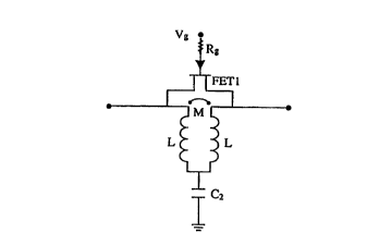
state (off-state), e.g. a PIN diode, a bipolar transistor or a "switch-FET".
In the case
shown in Fig. 8, the switching element is a first field effect transistor FET
1 which is
optimised to take, in dependence on its control voltage, two distinct states.
In the
one case, the transistor is biased to a conductive state, V~ = 0 . The
transistor then
corresponds to a very low resistance and the circuk behaves as a short
transmis-
sion line shunted with CZ .
in the second case, the transistor is biased so as to be fully depleted, IV~I
> ~VPI ,
where VP is the pinch-off voltage of the transistor. The transistor then
corresponds
to a capacitor. If the transistor parameters are selected such that the
capacitance of
the transistor is C~ , the circuit obtains, according to the derivation which
results in
equation (18}, a group delay which is independent of the frequency in a wide
frequency range.
This results in the circuit, in dependence on the control voltage to the
transistor,
taking one of finro states, in the first the group delay is very short and in
the other
long, which is shown in Fig. 7.
The shunt capacitor C2 , however, is normally not small enough to give a high
impedance to the line when the first field effect transistor FET 1 is in the
first state.
This results in a deterioration of the scattering properties, especially at
high
frequencies. A solution to this is to connect a second switching element, of a
type
similar to the first one, in series with the capacitor C2 . This second
switching
element is driven complementarily with the first, i.e. when the first is
conductive, the
second is fully depleted and vice versa. in this way, the line becomes shunted
by a
high impedance compared with CZ only. Fig. 8 shows a variant of this advanta-
geous embodiment of the invention with a second field effect transistor, FET
2,
optimised to take, in dependence on its control voltage, two distinct states,
as the
second switching element.
Two examples of a concrete layout for a self-switched artificial line in a
planar
monolithic circuit technique are shovm in Figs 9 and 10. In this case, the cut-
off
frequency is selected to be 18 GHz and the characteristic impedance to be 50
SZ .
The desired element values are the same in the two examples. The embodiments
CA 02315075 2000-06-16
WO 99135'740 PCT/SE98/02021
8
result in different group delay owing to the different geometric design of the
circuits,
which will be described below. The embodiments in the Figures are drawn accord-
ing to scale for accomplishment on a 100 Nm-thick GaAs substrate having the
permitivity 12.8.
Fig. 9 shows an embodiment in which the largest possible difference in group
delay
between the two states of the circuit is desired. The circuit has an input 1
and an
output 2. The inductances and the mutual inductance are realised as coupled
microstrip lines 3. The coupled microstrip lines are arranged such that the
short-
circuited shunt formed of FET 1 = 4a in the conductive state (i.e. when the
cinxrit
takes the state with a short group delay) is the shortest possible
transmission path
between input 1 and output 2. This is achieved by using two insulating
crossovers
5a and 5b. To earth extends CZ , designed as a plate capacitor 6, usually an
MIM,
in series with FET 2 = 4b, whose source is connected with a via hole 7 to the
ground plane of the circuit. The bias of FET 1 and FET 2 is applied to the
bonding
pads 8a and 8b, respectively, and is supplied to the gate via the respective
resistors
9a and 9b which are here designed as doped channels in the substrate with
controlled resistivity.
Fig. 10 shows an embodiment in which a smaller difference in group delay
between
the two states of the circuit is desired. The circuit has an input 1 and an
output 2.
The inductances and the mutual inductance are realised as coupled microstrip
tines
3. The short-circuited shunt formed of FET 1 = 4a in conductive state (i.e.
when the
circuit takes the state with a short group dealy) is here a comparatively
longer path
between input 1 and output 2 by one of the coupled microstrip lines 3b being
included in the shunt between the input and the output. In this case only one
insulating crossover 5 is necessary. To earth extends C2 , designed as a plate
capacitor 8, usually an MIM, in series with FET 2 = 4b, whose source is
connected
to a viahole 7 to the earth plane of the circuit. The bias of FET 1 and FET 2
is
applied to the bond plates 8a and 8b, respectively, and is supplied to gate
via the
respective resistors 9a and 9b, which are here designed as doped channels in
the
substrate with controlled resistivity.
The layout according to Figs 9 and 10 is cascadable, and therefore a composed
artificial line can be effected. Fig. 11 shows an example of cascade-coupled
self
switched artificial lines. By the control voltage to the respective first
field effect
transistor and, if necessary, the respective second held effect transistor, is
applied
to the different artificial lines in series via intermediate impedances R, the
respeo-
CA 02315075 2000-06-16
FCT,'S!= y6102G2
~'''' ~'.v~a:~h Pa'~~nt Office
~;:T~In'~r~:; i~n~l .l~plica'ion .
g 10 -OZ-1999
tive artificial line changes its state in tum at an increasing control
voltage, see Fig.
12. Thus, only one control wire is required.
Regarding a continuously tunable artificial tine which can be used alone or
together
with the self switched artificial line as stated above, it can be realised in
a manner
similar to that of the self switched artificial line. The theoretical values
of the circuit
elements are calculated in a manner corresponding to the previous manner. For
a
given characteristic impedance, element values are selected by first selecting
a
range within which the group delay GD should be tunable and transferring, via
the
diagram in Fig. 5, this to a range of the cut-off frequency f~. Then a cut-off
frequency is selected in the middle of this range. L and M are selected, based
on
the selected cut-off frequency, according to equation (18) and Fig. 5.
Finally the continuously tunable group delay is achieved by the capacitors C,
and
C2 in the two-port network according to Fig. 3a being replaced by varactors,
see
Fig. 13. The varactors are selected such that their capacitances C~ and C2 are
variable and follow the curves in Fig. 5 in the range for the desired
variation of the
group delay. The inductances L and the mutual inductance M will not follow the
relation exactly, and therefore the properties of the circuit are slightly
deteriorated.
In a variation of the group delay within the range of 5-15 ps, the
deterioration of the
input and output impedance is normally acceptable. It is in this case more
correct to
speak about an essentially frequency-independent mirror impedance (quasi
constant-R ... ).
Fig. 15 illustrates an example of a layout for a tunable artificial line. The
circuit has
an input 1 and an output 2. The inductances and the mutual inductance are
realised
as coupled microstrip lines 3. The voltage-controlled capacitance C"~ is
designed
as a varactor consisting of a field effect transistor 4a where the drain and
source
are interconnected and the bias for tuning is applied to its gate. The voltage-
controlled capacitance C"2 is also designed as a varactor 4b composed in the
same manner as the first-mentioned varactor 4a. The drain and source of this
varactor 4b are connected to the ground plane of the circuit with a via hole
7. The
design uses an insulating crossover 5. The voltage for tuning of C"~ and C~2
is
applied to the bonding pads 8a and 8b respectively and is supplied to the gate
via
the respective resistors 9a and 9b which are here designed as doped channels
in
the substrate with controlled resistivity. Two MIM capacitors 10a and 10b have
been
introduced for the varactors to be biased.
CA 02315075 2000-06-~6 l AMENDED SHEET