Note: Descriptions are shown in the official language in which they were submitted.
CA 02315132 2000-08-04
Bower-Zhou-Zhu 3-3-50 -1-
METHOD FOR FABRICATION OF PATTERNED
CARBON NANOTUBE FILMS
BACKGROUND OF THE INVENTION
Field of the Invention
The invention relates to devices comprising carbon nanotube
films.
Discussion of the Related Art
Carbon nanotubes have interesting electronic properties and offer
o potential for use in electronic devices and in interconnect applications.
Carbon nanotubes also feature high aspect ratios (> 1000) and
atomically sharp tips which make them ideal candidates for electron
field emitters. To realize these potential applications, there is a need to
process nanotubes into useful forms such as thin films, and,
advantageously, patterned thin films.
Carbon nanotubes are currently being produced by a variety of
different techniques such as arc-discharge, laser ablation and chemical
vapor deposition (CVD). (See S. Iijima, Nature, Vol. 354, p. 56 (1991);
T.W. Ebbesen and P.M. Ajayan, Nature, Vol. 358, p. 220 (1992); and B.I.
2o Yakobson and R.E. Smalley, American Scientists, Vol. 85, p. 324 (1997).
The as-deposited material, however, is usually in the form of loose
powders, porous mats, or films with poor adhesion. These forms of
nanotubes do not lend themselves to convenient preparation of robust
adherent nanotube thin film structures. The difficulty in preparing an
adherent film of nanotubes is believed to be due to the perfect structure
associated with carbon nanotubes, which contain essentially no dangling
bonds and few defect sites. As a result, nanotube films tend to exhibit
poor adhesion, even to the point of being easily removed by contact or by
air flow (e.g., an air duster).
3o Patterned nanotube films have been reported by Fan et al.,
Science, Vol. 283, p. 512 (1999), and Xu et al., Appl~Ph~s. Lett., Vol. 74,
CA 02315132 2000-08-04
Bower-Zhou-Zhu 3-3-50 -2-
p. 2549 (1999). These references describe use of direct deposition
techniques such as CVD, in which substrates are selectively patterned
with catalyst metals and then nanotubes are grown in the patterned
areas. These techniques, however, produce films with poor adhesion.
s The techniques also expose the substrates to a reactive and high-
temperature deposition environment, which is both inconvenient and
harmful to actual device structures. In addition, the techniques are
limited to the patterned growth of multi-wall carbon nanotubes
(MWNTs), because CVD typically produce MWNTs on catalytic
o substrates.
Thus, there is a desire to develop more convenient and versatile
methods for patterning carbon nanotube films with adequate adhesion,
to allow formation of more useful and robust device structures.
is SUMMARY OF THE INVENTION
The invention provides a method for fabricating adherent,
patterned carbon nanotube films. (Adherent indicates that the adhesion
strength of the film exceeds scale 2A or 2B according to ASTM tape
testing method D3359-97.) According to the invention, a substrate is
2o patterned with a carbide-forming material, a carbon-dissolving material,
or a low melting point metal (i.e., about 700°C or less). Carbon
nanotubes are then deposited onto the patterned substrate, e.g., by
spraying or suspension casting. The nanotubes have relatively poor
adhesion to either the substrate material or the patterned material at
25 this stage. The substrate is then annealed, typically in vacuum, at a
temperature dependent on the particular patterning material, e.g., a
temperature at which carbide formation occurs, at which carbon
dissolution occurs, or at which the low melting point metal melts. The
annealing thereby provides an adherent nanotube film over the
3o patterned areas, while the nanotubes deposited onto the non-patterned
CA 02315132 2003-10-06
-3-
areas are easily removed, e.g., by blowing, rubbing, brushing, or
ultrasonication in a solvent such as methanol. This process provides an
adherent nanotube film in a desired pattern. The patterned films are useful
for a variety of devices, including vacuum microelectronic devices such as
flat panel displays, as well as other structures, e.g., nanotube
interconnects.
In accordance with one aspect of the present invention there is
provided a process for fabricating a patterned, adherent carbon nanotube
film, comprising the steps of: providing a substrate; providing a patterned
material on the substrate, the material being selected from the group
l0 consisting of carbon-dissolving materials, carbide-forming materials, and
metals having a melting point of about 700°C or less; depositing carbon
nanotubes onto the substrate; annealing the substrate to promote adherence
of the nanotubes to the patterned material; and removing at least a portion of
the nanotubes located on the non-patterned area of the substrate.
In accordance with another aspect of the present invention there is
provided a device comprising: a substrate; a patterned material on the
substrate; and an adherent carbon nanotube film located on the patterned
material, the film comprising pre-formed nanotubes adhered to the patterned
material, wherein the patterned material is a carbon-dissolving material and
2o a carbon-containing solid solution adheres the nanotubes to the patterned
material, or the patterned material is a carbide-forming material and a
carbide adheres the nanotubes to the patterned material, or the patterned
material is a metal having a melting point of about 700°C or less and
at least
a portion of the nanotubes are physically embedded in the patterned
material.
CA 02315132 2003-10-06
-3 a-
BRIEF DESCRIPTION OF THE DRAWINGS
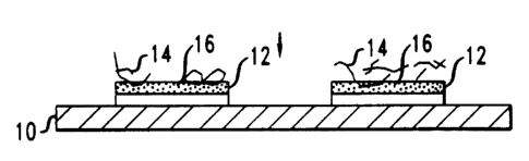
Figs. lA-1D illustrate the process of the invention.
Fig. 2 is an optical micrograph of a patterned nanotube film
fabricated according to the invention.
Figs. 3A and 3B reflect Raman Spectroscopy data indicating the
patterned nature of nanotube films fabricated according to the invention.
DETAILED DESCRIPTION OF THE INVENTION
The invention provides a process for fabricating patterned, adherent
carbon nanotube films. One embodiment of the process is shown in
l0 Figs. lA-1D. A flat substrate 10 is first provided. The substrate 10 should
be substantially non-reactive with carbon, e.g., not carbide-forming or
carbon-dissolving, and should also have a relatively high melting point,
typically at least 1000°C. Examples include Si02 (including Si wafers
having an oxidized surface layer), indium tin oxide (ITO), A1203, Cu, and Pt.
As reflected in Fig. 1A, a material 12 is deposited onto the substrate
10 in a pattern desired for the nanotube film. The patterning material 12 is
selected from (a) carbon-dissolving materials, (b) carbide-
CA 02315132 2000-08-04
Bower-Zhou-Zhu 3-3-50 -4-
forming materials, and (c) low melting point (about 700°C or less)
metals. Carbon-dissolving materials are known in the art, as reflected,
for example in T.B. Massalski, Binary Alloy Phase Dia ams, Vol. I,
ASM International, and include elements such as Ni, Fe, Co, and Mn.
Carbide-forming elements are similarly known in the art, as reflected in
Massalski, s. upra, and include elements such as Si, Mo, Ti, Ta, W, Nb,
Zr, V, Cr, and Hf. Typical low melting point metals include Al, Sn, Cd,
Zn, and Bi. The thickness of the patterning material 12 is typically 10 to
100 nm. The patterning material is deposited by any suitable technique,
e.g., sputtering, evaporation, or chemical vapor deposition. Conventional
lithographic processes are generally used to provide the desired pattern.
Carbon nanotubes 14 are then deposited onto the patterned
substrate 10, as reflected in Fig. 1B. (Only a few nanotubes are shown,
for representative purposes, in the drawing - in practice, nanotube
~5 coverage would be much more dense.) The nanotubes are typically
deposited by suspension casting or spray coating. Suspension casting is
generally performed by placing the substrate into a nanotube suspension
made up of nanotubes and a solvent such as methanol, and allowing the
solvent to evaporate. Spray coating is performed by spraying such a
2o suspension onto the substrate (which is typically heated) using an air
gun, and allowing the solvent to evaporate. Both methods tend to
provide relatively uniform thin films of randomly oriented nanotubes.
As reflected in Fig. 1C, the substrate 10 is then annealed,
generally in vacuum ( 10-6 torr or less). The temperature of the anneal is
25 selected based on the patterning material 12. Specifically, the
temperature is chosen to promote carbon dissolution, carbide formation,
or melting of the patterning material 12. The anneal is generally
performed 30 minutes to 24 hours, depending on the particular
patterning material. By inducing carbon dissolution, carbide formation
30 or melting at the areas where the nanotubes 14 contact the patterning
CA 02315132 2000-08-04
Bower-Zhou-Zhu 3-3-50 -5-
material 12, an area 16 of enhanced adherence between the nanotubes
14 and patterning material 12 is created. Specifically, for carbide-
forming material, a carbide is formed by reaction of the material and at
least a portion of the nanotubes. For carbon-dissolving material, a
metal-carbon solid solution is formed by reaction of the material and at
least a portion of the nanotubes. And for low melting point metals, at
least a portion of the nanotubes become physically embedded in a molten
metal layer and then held in place upon cooling.
As reflected in Fig. 1D, the nanotubes deposited directly on the
1o substrate 10 material are removed after annealing. Because the
nanotubes have relatively poor adherence to the substrate 10 material,
removal is relatively easy. Removal is capable of being performed by
blowing, rubbing, or brushing the surface of the substrate 10, or by
ultrasonication in a solvent such as methanol. It is possible to combine
t5 these techniques. Typically, the substrate is ultrasonicated without
blowing, rubbing, or brushing. Ultrasonication, when performed without
any other removal technique, is generally performed for 0.5 to 24 hours.
The thickness of the resultant adherent, patterned nanotube film
is generally 100 to 1000 nm. The adhesion strength of the resultant
2o patterned nanotube films is sufficient to exceed the 2A or 2B scale in the
ASTM tape test D3359-97.
The patterned nanotube films are useful in a variety of
applications, including vacuum microelectronic devices such as flat panel
displays, as well as novel applications such as interconnects in silicon-
25 based devices.
The invention will be further clarified by the following examples,
which are intended to be exemplary.
Example 1
A silicon substrate with an oxidized surface was provided. A1 pads
3o having an area of 100 x 70 ~m and a thickness of 50 nm were patterned
CA 02315132 2000-08-04
Bower-Zhou-Zhu 3-3-50 -6-
onto the substrate surface by thermal evaporation, using a shadow
mask. Single wall carbon nanotubes were obtained. The nanotubes had
been fabricated by laser ablation with bundle diameters of 10 to 30 nm
and lengths of 2 to 10 Vim, and were then purified using an ultrasonically
assisted filtration technique (see, e.g., K.B. Shelimov et al., "Purification
of Single Wall Nanotubes by Ultrasonically Assisted Filtration," Chem.
Phys. Lett., Vol. 282, p. 429 (1998)). The nanotubes were deposited onto
the patterned substrate by spraying. The substrate was then vacuum
annealed at 700°C for 30 minutes (the melting point of Al is about
to 660°C), and ultrasonicated in methanol for two hours. The resulting
patterned nanotube film is shown in Fig. 2, with coated pads 20, and
uncoated substrate surface 22.
Example 2
~5 A silicon substrate with an oxidized surface was provided. Fe
pads having an area of 70 x 70 ~,m and a thickness of 20 nm were
patterned onto the substrate surface by sputtering, using a shadow
mask. Single wall carbon nanotubes were obtained as in Example 1.
The nanotubes were deposited onto the patterned substrate by spraying.
2o The substrate was then vacuum annealed at 800°C for 30 minutes, and
ultrasonicated in methanol for 2 hours. A portion of the resulting
structure - coated Fe pad 30 and uncoated substrate surface 32 - is
shown in Fig. 3A.
To confirm that the nanotubes remained intact after the
25 annealing and ultrasonication, Raman spectroscopy was performed. The
graphitic carbon-carbon vibration mode at about 1580 cm 1 is indicative
of the presence of the nanotube structure. As shown by the Raman
spectroscopy results in Fig. 3B, the spectra taken over the Fe pad show
nanotubes, while the spectra off the pad indicates the absence of
3o nanotubes.
CA 02315132 2000-08-04
Bower-Zhou-Zhu 3-3-50 -7-
Other embodiments of the invention will be apparent to those
skilled in the art from consideration of the specification and practice of
the invention disclosed herein.