Note: Descriptions are shown in the official language in which they were submitted.
CA 02315417 2000-08-10
1
DESCRIPTION
ELECTRET CAPACITOR MICROPHONE
BACKGROUND OF THE INVENTION
Field of the Invention
The present invention relates to an electret capacitor
microphone.
Prior Art
Electret capacitor microphones are often provided with
a thin diaphragm having a thin metal film facing toward an
opening in a metal casing and a fixed electrode opposed
thereto, and utilize the principal of a change in capacity
between the diaphragm and the fixed electrode dependently
on the vibration of the diaphragm due to a sound wave. The
diaphragm utilizes a thin metallized electret material on a
surface thereof, and a capacitor is formed between the
diaphragm and the fixed electrode. A change in capacity is
converted into a current or voltage change through a solid
state device, the sound wave being fetched as an electric
signal.
Conventional electret capacitor microphones have been
provided in a cylindrical metal casing 5 which disposes a
diaphragm 4 made of an electret material with a metal layer
deposited or other method on the surface and has a sound
CA 02315417 2000-08-10
2
hole 21 in the central part of an upper surface facing to
the diaphragm 4, as shown in Fig. 13. In the casing, a
fixed electrode 6 is fixed just behind the diaphragm 4 with
a capacitance gap 3?_ through a thin gap ring spacer 61
between the fixed electrode 6 and the diaphragm 4.
Furthermore, a depressed dielectric 27 accommodating a solid
state device 8 and a printed circuit board 29 are located in
a lower part of the casing 5, and the casing is crimped to a
peripheral edge 52 on the back face of the printed circuit
board 29, using a crimping portion 52 of the opening of the
metal casing 5.
In the conventional example, an input lead 81 of the
solid state circuit device 8 is connected to a fixed
electrode 26, and an output lead 82 penetrates through the
special dielectric 27 and the printed circuit board 29 and
is connected to a pad electrode 83 on a bottom face. On the
other hand, the diaphragm 4 is conducted to the metal casing
5 through a film ring 41.
Recently, electret capacitor microphones have been
required to be light and small-sized. However, in the
conventional microphone technique, a large number of parts
have been required and the thickness the crimping portion
and the pad electrode could not be reduced.
Moreover, in the conventional microphones, since the
dielectric and the printed circuit board have been utilized,
CA 02315417 2000-08-10
3
it has been impossible to satisfy the demand for a reduction
in size and weight of the whole microphone.
Conventional electret capacitor microphones are not
suitable for mass-production and have had a low productivity.
The reason is because parts from the fixed electrode 6 to
the printed circuit board 29 are previously assembled as an
amplifier block and each part of the assembly is
individually disposed in the metal casing 5 and is finally
crimped with the crimped portion 52.
In the conventional electret capacitor microphones,
since the metal casing is crimped with a substrate, and then
the uncertainty of fixation of each part causes microphone
failure in use and reduces the yield of the microphone
products.
Conventionally, soldering pad electrodes 83, which are
takeoff connection portions, have been attached neat a
center of the circuit board 29 so that it has been hard to
carry out mounting a solid circuit device 8 on the circuit
board 29 by soldering the pad electrode 83, and the
conventional microphones have had a risk of short-circuiting
the circuit board.
A main component of the microphone restricting a
reduction in size has been a metal casing 5. A solid circuit
device B including a transistor or an integrated circuit
which normally has a square shape is accommodated on the
CA 02315417 2000-08-10
4
circuit board with useless space because a conventional
metal casing is cylindrical. In addition, the cylindrical
metal casing 5 is hard to handle for mounting and to
position. Furthermore. even if a sound hole is to have a
complicated shape, processing is hard.
The metal casing 5 is apt to transmit a surrounding
mechanical vibration, has an adverse influence on the
diaphragm and supplies a noise to an electric signal,
resulting in a deterioration in microphone performance.
Since the output leads was provided through the printed
circuit board, pad electrodes for soldering was required to
bury holes through which the leads pass airtightly.
A diaphragm 24 is a membrane of fluoro-polymer membrane
such as polyfluoroethylene, polypropylene (FEP), or
polyester polymer such as Mylar (registered trademark), and
has a thermal resistance limited. Therefore, it has been
hard to solder the microphone onto the printed circuit board
by heating.
SUMMARY OF THE INVENTION
An object of the present invention is to provide a
compact and thin electret capacitor microphone by reducing
the number of parts constituting the capacitor microphone as
much as possible.
Another object of the present invention is to provide
CA 02315417 2000-08-10
an electret capacitor microphone capable of being assembled
with mechanical fixation and electrical connection of parts
carried out readily.
Another object of the present invention is to provide
5 an electret capacitor microphone capable of being simply and
reliably mounted in a small size onto another printed
circuit board.
The elecret capacitor microphone of the present
invention includes a casing formed of a dielectric and
having a bottomed hollow portion which accommodates a
combination of a diaphragm and a fixed electrode apart from
each other at regular capacitance interval and a solid state
device for converting, into an electric signal, a change in
an electrostatic capacity between a diaphragm and the fixed
electrode, hereby forming an electret capacitor microphone.
Electret capacitor microphone will be hereinafter
referred to as microphone, simply.
A dielectric casing can directly fix the parts in the
hollow portion, eliminating the need for use of a printed
circuit board for fixing a special insulator member and
solid state circuit according to the conventional example,
thereby decreasing the number of parts to be used.
Furthermore, an opening of the casing can be covered
with a metal cover having a sound hole to penetrate sound
from the outside of the casing to the interior of the hollow
CA 02315417 2000-08-10
6
and fixed by bonding to the periphery of the opening. As a
result, the microphone according to the present invention
has a high mass-productivity.
Furthermore, in the microphone of the present invention,
the casing may contain the solid state device in parallel to
the combination of diaphragm and fixed electrode in its
hollow. The combination and the solid state device are
arranged laterally so that the whole thickness of the casing
is further reduced to make the microphone much thinner.
In the present invention, preFe.rably, the hollow
portion of.the casing may be divided into two partial hollow
portions, in which case the combination of the fixed
electrode and the diaphragm may be located in one of the
hollow portions and the solid state device is placed in the
other hollow portion.
Furthermore, it is preferable that the microphone
according t~ the present invention should have cover for
covering the opening of the hollow portion. The cover can
also be shared by the fixed electrode, where the cover and
the diaphragm are arranged facing to each other to
constitute a capacitance gap.
In the present invention, one or more recesses for
absorbing a sound preferably may be formed on the bottom of
the hollow portion of casing, to eliminate an influence on
the diaphragm of a reflected wave to be generated with
CA 02315417 2000-08-10
7
deduced volume of the hollow portion. The recesses means a
depessed portion which is at a lower level than a bottom
level of the hollow portion accommodating the solid state
device. The vibration of the diaphragm caused by the sound
wave makes a wave to the back side toward the hollow bottom.
The recess serves to increase a volume under the diaphragm
the in the casing to form a release passage for the
reflected wave which passage prevents the reflected wave of
the diaphragm from interference with the diaphragm, and to
compensate for a deterioration in sound-vibration fidelity
of the diaphragm.
In the present invention, moreover, the casing can
directly apply leads, or interconnections on an outer
surface and/or inner surface thereof by utilizing dielectric
properties. The dielectric casing may be provided with pad
electrode on the outside of the case to be connected to
these leads. preferably, the pad electrodes can be applied
on both sides of the bottom surface of the casing with a
simple structure, and then the case can be mounted on other
printed circuit boards by soldering the pad electrodes to
the corresponding pad electrodes arranged on the circuit
board.
In the present invention, furthermore, one or two
stepped portions preferably may be provided on the inner
wall surface of the hollow portion of the casing to set a
CA 02315417 2000-08-10
8
diaphragm and a fixed electrode wherein their peripheral
edge portions are mounted on the stepped portions. These
parts can be conveniently fixed only by bonding such as
adhesion or solder bonding, without using other special
means for fixing., in the hollow portion, resulting in
reduction of the number. of the parts.
In the present invention, moreover, it is.preferable.
that the casing, particularly, the hollow portion should
have a rectangular cross section. The square shape can be
coincident with the external shape of the solid state device
or integrated circuit to be accommodated.
Furthermore, the square casing can cause the microphone
to be easily handled in a manufacturing process and the
completed microphone to be positioned precisely on a wiring
board.
BRIEF nESCRIPTION OF THE DRAWINGS
The present invention will be described below in more
detail with reference to the accompanying drawings, in
which:
Fig. 1A is a longitudinal sectional view showing a
microphone according to an embodiment of the present
invention;
Fig. 1B is a top view showing the microphone
illustrated in Fig. lA;
CA 02315417 2000-08-10
' ' 9
Fig. 1C is a bottom view showing the microphone
illustrated in Fig. lA;
Fig. 1D is a perspective view showing a cover according
to another embodiment;
Fig. 1E is a longitudinal cross-sectional view showing
a microphone according to an embodiment of the present
invention;
Fig. 2 is a longitudinal sectional view showing the
microphone according to an embodiment of. the present
invention in which a cover is also used as a fixed
electrode;
Figs. 3A to 3C are sectional views showing a casing for
the fixation of a solid state device in the casing according
to an embodiment of the present invention;
Figs. 9A and 4B are sectional views showing the casing
for the fixation of the solid state device in the casing
according to an embodiment of the present invention;
Fig. 5 is a perspective view showing a ceramic
substrate for dicing a large number of casings;
Fig. 6A is a longitudinal sectional view showing a
microphone in which two hollow portions are provided and a
capacitor portion and a solid state device are arranged
thereon in parallel according to the embodiment of the
present invention;
Fig. 6B and 6C show a top view and a bottom view,
CA 02315417 2000-08-10
' 10
respectively, of the microphone illustrated in Fig. 6A;
Fig. 7 is a longitudinal sectional view showing the
microphone according to the embodiment illustrated in Fig. 6,
in which a cover is also used as a fixed electrode;
Fig. 8 is similar to Fig. 6A, in which a capacitor
portion and a solid state device are provided in parallel in
a single hollow portion according to the embodiment of the
present invention;.
Fig. 9 is similar to Fig. 7, in which a cover is also
used as a fixed electrode in the microphone illustral:ed in
Fig. 8;
Fig. l0A is the same as Fig. lA illustrating the
embodiment in which a concave portion is formed on the
bottom of the hollow portion of the casing;
Fig. lOB is the same as Fig. lE illustrating the
embodiment in which a concave portion is formed on the
bottom of the hollow portion;
Figs. 11A to 11C are top views showing the casing in
which the concave portion is formed on the bottom of the
hollow portion;.
Fig. 12A is a sectional view showing a casing according
to another embodiment in which a concave portion is formed
in the hollow portion of a casing;
Fig. 12B is a partial perspective view showing the
inside of the hollow portion of the casing according to the
CA 02315417 2000-08-10
11
embodiment utilizing a portion between the divided steps as
a concave portions and
Fig. 13 is a longitudinal sectional view showing a
conventional microphone_
PREFERRED EMBODIMENTS OF THE INVENTION
A casing to be used for a microphone according to the
present invention is formed of a dielectric material. For
the dielectric material, ceramics (including glassy, polymer
or a composite material is used. The casing is formed of
the above-mentioned material to be a bottomed hollow member.
Typically, the hollow portion is provided with a
diaphragm on the opening side and a fixed electrode
therebehind opposite to the diaphragm with a very small gap.
The diaphragm is a thin film made of an electret material
having a thin metal layer applied to a surface. For the
electret material, fluoro-polymer such as FEP and polyester
are used. A metal plate is utilized for the other fixed
electrodes. The diaphragm and the fixed electrode
constitute a capacitor, and a solid state device is
connected to the diaphragm and the fixed electrode in order
to convert a change in a capacity caused by a sound wave
vibration into a change in a voltage or current. A cover is
attached to the opening of the hollow portion, and a proper
sound hole penetrates through the cover.
CA 02315417 2000-08-10
12
In the present invention, the arrangement of the solid
state device can have some structures.
First of all, the solid state device is provided on the
bottom behind the diaphragm and the fixed electrode in the
same hollow portion accommodating the diaphragm and the
fixed electrode.
Secondly, the solid state device is provided on the
bottom in a transverse direction with respect to the
diaphragm and the capacitor of the fixed electrode in the
same hollow portion accommodating the diaphragm and the
fixed electrode. Consequently, the casing can be thinned
through a first structure. '
Thirdly, the casing is provided with a separate hollow
portion differently from the hollow portion accommodating
the diaphragm and the fixed electrode, and the solid state
device is provided in the separate hollow portion.
The opening of the hollow portion is covered with a
plate-shaped cover. A metal plate having a sound hole 21 in
a position opposite to the diaphragm is utilized for the
cover.
Preferably, the hollow portion of the casing forms a
rectangular cross section. On the other hand, the diaphragm
and the fixed electrode may comprise rectangular outer edges
such that they are coincident with the hollow portion having
a rectangular section. In particular, the solid state
CA 02315417 2000-08-10
' 13
device having a rectangular external shape is conveniently
accommodated in the bottom portion.
It is preferable that the hollow portion should form a
stepped portion to stop and support the diaphragm and/or the
fixed electrode on the outer edge. The fixed metal and the
diaphragm have such rectangular shapes that peripheral edges
can be mounted on the stepped portion. The fixed metal and
the diaphragm are provided apart from each other with a
capacitance gap through a spacer therebetween, thereby
forming a capacitor having a small capacity.
The fixed electrode or the diaphragm has a peripheral
edge mounted on the upper surface of the stepped portion and
is conductively joined and fixed, with proper bonds, to a
separate lead on the inner surface in the hollow portion.
First Embodiment
In this example, a solid state device is provided on a
bottom below a diaphragm and a fixed electrode in the same
hollow portion accommodating the diaphragm and the fixed
electrode.
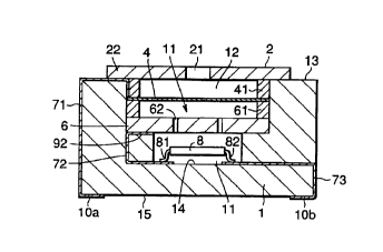
A microphone shown in Fig. lA utilizes a rectangular
box-shaped casing 1, and a hollow portion 11 in the casing 1
has a rectangular section and the opposite side of the
bottom is opened. A stepped portion 92 is formed on the
inner surface of the hollow portion 11.
CA 02315417 2000-08-10
19
A fixed electrode 6 is mad of a metal with through
holes 62 passing therethrough and is mounted on the stepped
portion 92 and is fixed thereto, and a diaphragm 4 is
mounted with a very small capacitor gap through a ring-
s shaped dielectric spacer 61 above the.fixed electrode 6,.
thereby constituting a capacitor. A peripheral edge portion
22 is bonded and fixed to an upper surface 13 of the opening
of the hollow portion 11 through a ring spacer 41.
Furthermore, a solid state device B is located ~n a
bottom 14 in the hollow portion 11 closer to the bottom side
than the stepped portion 92. In this example, an input lead
81 and an output lead B2 of the solid state device 8 are
directly fixed to conductive paths 72 and 7~3 applied to the
bottom through means such as brazing or conductive adhesion.
The diaphragm 4 and the fixed electrode 6 are connected
to the solid state device 8 through the conductive path
provided on the inner surface or outer surface of the casing
1. The solid state device 8 converts a change in a capacity
between the diaphragm 9 and the fixed electrode 6 caused by
an input sound wave into a change in a voltage and current,
and pre-amplifies the same depending on the circumstances.
The output of the solid state device 8 is connected to an
electronic circuit provided on a separate wiring board.
As an example of the connection, for example, a proper
conductive path 72 is provided on the inner surface from the
CA 02315417 2000-08-10
' ~ 15
stepped portion 92 to the bottom, and the fixed electrode 6
is mounted on the stepped portion 92 and is joined to the
conductive path through bonds. Such a bonding material
includes solders, brazes and conductive adhesives.
The casing 1 may have a conductive path 71 provided on
the outer surface. The conductive path can utilize a
conductive paste layer applied on the casing surface and a
through hole filled with a conductive paste. A green sheet
including the conductive paste is provided so that a
conductive film can be formed on a surface or an inner
surface .
An example of the conductive path is shown in Figs: lA
and 1B. In the conductive path connected to the diaphragm,
the vibration film 4 comes in contact with the film ring 41,
and the film ring 41 is connected to a pad electrode l0a on
a bottom surface through the metal film of an opening
surface 13 of the opening of the hollow portion 11 and the
succeeding conductive path 71 on the outer surface. The
opening end face 13 of the casing 1 has a metal film
metallized and is also bonded to the metal cover 2 with
solders, brazes, conductive adhesives and the Like.
For the fixed Plectrode 6, the conductive path 72
including the stepped portion 92 for stopping the fixed
electrode is formed on the inner surface of the hollow
portion and is connected to the input terminal 81 of the
CA 02315417 2000-08-10
16
solid state device 8 in the bottom portion. Furthermore,
the conductive path 73 connected to the output terminal 82
of the solid state device is led to the outside of the
casing 1 and is connected to another pad electrode lOb.
In this example, the pad electrode l0a connected to the
diaphragm 4 is grounded, and the conductive path 71 can
serve as an electrostatic shield if the outer surface of the
casing is covered with a proper area. The other pad
electrode lOb is utilized as the output terminal of the
solid state device 8 and is also used as a power source at
the same time. According to the electret capacitor
microphone according to the present embodiment, the pad
electrodes l0a and lOb can easily be mounted on a separate
printed circuit board on both sides of the bottom surface of
the casing 1 as shown in Fig. 1C.
The electret capacitor microphone according to the
present invention uses the dielectric casing 1. As compared
with a conventional structure shown in Fig. 12, therefore, a
printed circuit board 29 mounting a dielectric 27 and an
electronic circuit 8 in the metal casing can be eliminated
and the number of parts can be decreased, resulting in a
reduction in a size.
According to the electret capacitor microphone in
accordance with the present invention, furthermore, the
elements are inserted and Lixed in order from the bottom
CA 02315417 2000-08-10
17
face side through the opening 12 in the hollow portion 11 of
the casing 1, and the opening is finally covered with the
cover 2. Consequently, a manufacturing process can be
simplified and mass production can be carried out easily,
The stepped portion 92 bonds the fixed electrode 6 into the
casing '1 and other parts can also be.bonded to the casing
reliably and easily. Thus, these elements can be fixed
strongly.
Furthermore, the casing 1 has the hollow portion taking
a rectangular cross section and can easily accept the
square-shaped solid state device 8, thereby preventing a
spatial waste. Consequently, the size of the whole
microphone can be more reduced. In addition, when the
microphone is to be mounted on the surface of another wiring
board, it can be easily handled because of the square shape
and can also be positioned on the wiring board readily.
The dielectric forming the casing 1 can use cerarmics
including, as main components, alumina, zirconia, rnullite,
silicon carbide, silicon nitride, aluminum nitride and the
like, and can particularly enhance a periodic damping
characteristic. The reason is that these ceramics have
greater vibration damping capacities as compared with a
metallic material. A ceramic casing is particularly used
for a portable telephone or the like, and can transmit an
external vibration to Lhe inside with difficulty and can
CA 02315417 2000-08-10
1B
enhance the signal-to-noise characteristic of the microphone.
In the present invention, furthermore, the rectangular
casing 1 can allow for the plate-shaped cover 2 and can
easily process the cover. Therefore, it is also use a
structure in which a mesh-shaped sound hole 21 is provided
as shown in Fig. 1D, for example. The sound hole 21 is
usually covered with a plane cloth (not shown) to prevent
foreign substances from entering. Thus, the mesh-shaped
sound hold 21 can omit the plane cloth.
lU As another embodiment, preferably, two stepped portions
92 may be formed on the casing 1, one of them fixing the
diaphragm~4 and the other fixing the fixed electrode 6 as
shown in Fig. lE. The two steps have an advantage that the
film ring 3 and the gap spacer 61 can be omitted.
Second Embodiment
Second Embodiment
In the present embodiment, a fixed electrode is also
used as a cover. In the example shown in Fig. 2, an opening
12 of a casing 1 is covered with a metal cover 2 having a
sound hole fixed to an upper surface 13, and the back side
~f the cover is provided with a diaphragm 4 through a
dielectric gap spacer 41. The diaphragm 4 is fixed to a
stepped portion 92 in a hollow portion. The cover 2 is
connected to a pad electrode l0a through a conductive path
CA 02315417 2000-08-10
19
71 provided on an outer surface, and the diaphragm 9 is
connected to a pad electrode lOb through a conductive path
72, a solid state device 8 and a conductive path 73 as
described above.
In the present embodiment, the cover 2 is also used as
the fixed electrode 6 to detect a change in an electrostatic
capacity between Lhe cover 2 (fixed electrode 6) and the
diaphragm 4. Consequently, the number of parts can be more
decreased and a size can be more reduced as compared with
those in Fig. 1.
Next, the structure of attachment of the solid state _
device B will be described. In the above-mentioned example,
an input lead 81 and an output lead 82 of the solid state
device 8 are mounted on the conductive paths 72 and 73
respectively, and are bonded with solders, brazes,
conductive adhesives or the like.
As shown in Fig. 3A, two stepped portions 92 and 921
may be provided on the inside of the box-shaped casing 1,
and the input lead 81 and the output lead 82 of the solid
state device 8 may be mounted on the stepped portion 92b and
may be bonded to the conductive path. Alternatively, the
solid state device 8 having no lead may be provided and may
be connected to a conductive path (not shown) through a wire
bonding 83 as shown in Figs. 3B and 3C.
In the present inveliLion, furthermore, the dielectric
CA 02315417 2000-08-10
' 20
casing 1 is used. Therefore, it can also be possible to
easily mount other electronic parts. As shown in Fig. 4A,
for example, another stepped portion 95 may be formed below
the solid state device B and another electronic part 89 may
be provided therein or a concave portion 96 may be formed in
an outer bottom portion 15 of the casing.l and the
electronic part 84 may be provided therein.
In a process of manufacturing an electret capacitor
microphone.according to the present invention, moreover, th,e
microphone can be mass-produced by using many fetching
methods. For example, as shown in Fig. 5, a large number of
hollow portions 11 are formed on a board 19 made of a
dielectric such as ceramics or glass, and dicing is carried
out along scribing lines 191. Consequently, each casing 1
can be obtained. Alternatively, each part may be
accommodated in each hollow portion 11 before the dicing and
the electret capacitor microphone may be fabricated, and the
dicing operation can be then carried out along the scribing
lines 191. The dicing operation along the scribing lines
191 is carried out by cutting through a scribing trench
formed on the board 19 in advance or cutting using a diamond
cutter, a laser beam or the like. By using such a method, a
large number of microphones can be produced collectively.
Third Embodiment
CA 02315417 2000-08-10
21
Fig. 6A shows a microphone comprising two independent
and adjacent hollow portions lla and llb separated though
partition walls in a casing 1 made of a dielectric. The
combination of a diaphragm 4 and a fixed electrode 6 is
provided in the hollow portion lla and a solid state device
8 is provided in the hollow portion llb. In this example,
both hollow portions lla and llb are covered with one plate-
shaped cover 2.
In the hollow portion 11, the fixed electrode.6 is
provided on a bottom face, a~stepped portion 92 is formed,
and a diaphragm 4 is provided on the upper surface of the
stepped portion through a capacitance gap with respect to
the fixed electrode 6. A thin film made of an electret
material having a metal layer formed thereon is utilized for
1~ the diaphragm 4. The solid state device 8 is directly
bonded to the bond face in the hollow portion llb. An
amplifier circuit or the like is formed on the solid state
device 8.
The cover 2 serves to close the two hollow portions lla
and llb and a sound hole 21 is opened in a portion
corresponding to the hollow portion lla.
In this example, the diaphragm 4 is bonded onto a
conductive path 74 formed in the stepped portion, the
conductive path is connected to a conductive path 71 on the
outer surface of the casing via a through hole 74, and is
CA 02315417 2000-08-10
22
connected to a pad electrode l0a on the bottom face.
The conductive path 71 is provided to cover a large
portion of the outer surface of the casing and is grounded.
Therefore, it is possible to carry out a shield against a
high frequency wave or an electrostatic shield.
Moreover, the fixed electrode 6 is conducted to the
conductive path 72 and. is connected to an input_terminal.81
of the solid state device 8, and a conductive path 75
connected to an output terminal 82 is led to an external
conductive path 73 of the casing 1 and is connected to
another pad electrode lOb. The input terminal 81 and. the
output terminal 82 of the solid state device 8 are subjected
to wire bonding between the conductive paths 72 and 75
provided in the stepped portion 92b of the hollow portion
llb, respectively.
Fig. 6C shows the arrangement of the pad electrodes l0a
and lOb on both sides of the bottom face of the casing 1.
It is also possible to easily carry out mounting on other
wiring boards and connection to a connecting pad electrode
on the board side.
As shown in Fig. 6B, an upper end face 13 of the casing
1 is metallized and is connected to the conductive path 71
on the external surface and is conductively bonded to the
metal cover 2 with conductive adhesives or the like.
Consequently, the cover 2 has the same potential as that of
CA 02315417 2000-08-10
23
the conductive path 71, that is, an earth potential.
Thus, the diaphragm 4 and fixed electrode 6 and the
solid state device 8 are accommodated in parallel.
Consequently, a thickness can be reduced. In the present
embodiment, furthermore, there is an advantage that the
solid state device 8 can be accommodated in the independent
hollow portion llb and can be sealed airtightly with the
cover.
Furthermore, the hollow portion has a square shape seen
in a plane and the casing 1 has a polygonal shape as a whole.
The hollow portion has such an advantage that a spatial
waste is not caused and the whole size can be more reduced
when the polygonal solid state device 8 is accommodated
therein. In addition, when the microphone is to be mounted
on a surface, the polygonal shape can give easy handling and
simple positioning.
Fig. 7 shows another variant in which the fixed
electrode 6 is also used as the cover 2. Two hollow
portions lla and llb are formed in the casing 1 through a
partition wall. A diaphragm 4 is provided in a stepped
portion 92 of the hollow portion lla in the casing 1. The
diaphragm 4 is connected to a pad electrode l0a through a
conductive path 72 and a solid state device 8 is
accommodated in the hollow portion llb, and the solid state
device is connected to a pad electrode lOb through
CA 02315417 2000-08-10
29
conductive paths 75 and 73. Moreover, the cover 2 is bonded
to the upper surface of an opening to cover the diaphragm,
and the cover is connected to the pad electrode l0a through
a conductive path 71 such that it can be utilized together
with the fixed electrode 6 for the diaphragm 4.
Fourth Embodiment
As another embodiment, in the embodiment shown in Fig.
8, one hollow portion 11 accepts the combination of a fixed
electrode 6 and a diaphragm 4 and a solid state device 8
provided at the side thereof. In this example, the fixed
electrode 6 is applied to the bottom surface of the hollow
portion 11 of the casing l, and the diaphragm 4 is provided
with a capacitor gap through a gap spacer 61. The diaphragm
bonds a conductive path 75 provided in a stepped portion 92
to a wire and is connected to a pad electrode l0a through a
conductive path 71. Moreover, the cover 2 is also connected
to the conductive path 71. On the other hand, the solid
state device 8 is provided on the bottom face of the hollow
portion 11 in parallel with the fixed electrode, and an
input terminal 81 of the solid state device 8 is wire bonded
to the fixed electrode 6, an output terminal 82 is wire
bonded to the conductive path 75 in the stepped portion 92,
and the conductive path 75 is connected to the other pad
electrode lOb through a conductive path 73.
CA 02315417 2000-08-10
With this structure, one hollow portion 11 is formed in
the casing and parts can be provided transversely.
Therefore, the casing can have a simple shape and
manufacture can easily be carried out.
5 Fig. 9 shows another variant in which a fixed electrode
6 is also used as a cover 2 by using a further.hollow
portion. A diaphragm 4 is provided through the gap spacer
61 below the cover 2 covering an upper surface 13 of a
casing 1, and is electrically connected to a pad electrode
10 lOb through a.conductive path 72, a solid state device B and'
conductive paths 75 and 73 via a film ring 3. Moreover,-the
cover 2 which is also used as the fixed electrode is
connected to another pad electrode l0a through the
conductive path 71.
15 While a conventional electret capacitor microphone
should require a thickness of approximately 2 mm, the
electret capacitor microphone according to the present
invention described above can have a thickness of I mm or
less, preferably 0.5 mrn or less.
Fifth Embodiment
In the present embodiment, a microphone is provided
with a recess on the internal wall of a hollow portion of a
casing. A stepped portion for fixing a diaphragm and a
fixed electrode in the hollow portion is provided in the
CA 02315417 2000-08-10
26
hollow portion, and a solid state device is fixed to the
bottom of the hollow portion. With such a structure, the
recess is positioned behind the diaphragm. The vibration of
the diaphragm caused by an input sound wave generates sound
wave vibration on the back side. However, the recess
increases a blank volume on the rear side to absorb or damp
a sound wave into the back side, Lhereby preventing the
interference of the sound wave on the back side with the
diaphragm and a deterioration in fidelity due to the
interference.of the diaphragm. The recess may be formed in
any portion of the inner surface of the hollow portion on
the rear side of the diaphragm, preferably, in the bottom on
the inside.
The microphone of this type comprises a stepped portion
92 on the internal wall of a hollow portion 11 of a casing 1
formed of a dielectric and a recess 12 is provided in the
bottom on the inside as shown in Figs. l0A and lOB. In the
example of Fig. 10A, a solid state device 8 is fixed to the
bottom portion, a fixed electrode 6 is provided in the
2o stepped portion 92, a diaphragm 9 is provided above the
fixed electrode through a ring-shaped spacer 61 forming a
capacitor gap, and a cover 2 through which a sound hole 21
penetrates is bonded to an opening.
Fig. lOB shows a variant of a microphone in which a
fixed electrode 6 provided with a recess 12 i5 also used as
CA 02315417 2000-08-10
27
a cover 2. A casing forms a stepped portion 92 supporting a
diaphragm in a hollow portion, and a recess is similarly
formed as a concave part in the bottom portion. An upper
end face 13 of a casing 1 is covered with a cover 2 which is
also used as the fixed electrode 6, and a diaphragm 4 is
fixed to the stepped portion 92 below the cover 2 through a
spacer 61 forming a capacitor gap so that a capacitor is
formed by the diaphragm 4 and the cover 2. A solid state
device 8 is fixed to the bottom portion. A recess 12 is
further provided in the bottom portion to damp a sound wave
on the back side through the diaphragm 9 and to prevent a
deterioration in characteristics.
Figs. 11A to 11C show various examples of the planar
shape of the recess 12. The recess 12 pan be formed to have
a rectangular shape on the bottom face of a hollow portion
11 (Fig. 11A) and can be formed circularly (Fig. 11B).
Furthermore, a part of the side surface of the recess may be
on the level with the internal wall of the hollow portion
(Fig. 11C). In any case, the recess 12 is not completely
covered with the solid state device 8 but is formed
spatially continuously with the hollow portion 11. Moreover,
the recess 12 may be provided in any of the wall surfaces of
the hollow portion 11 and is preferably formed on a bottom
face opposed to the diaphragm 9.
Moreover, the recess 12 is provided. Consequently,
CA 02315417 2000-08-10
28
when the solid state device 8 is to be joined through
solders, brazes, conductive adhesives or the like, these can
act as an antirunning material and can also contribute to a
reduction in a whole weight. Alternatively, other
electronic parts can be mounted on the recess 12. In
respect of the strength of the casing 1, a portion of the
casing where the recess 12 is formed requires a thickness of
0.1 mm or more.
As a further embodiment, in Fig. 12A, a stepped portion
92b in the hollow portion of the casing 1 is formed only one
of sides. Consequently, the volume of the hollow portion 11
is increased. Moreover, the stepped portion 92 is divided
into two stepped portions 921 and 922. Consequently, a
space 121 between the two stepped portions can he utilized
for a recess.
Sixth Embodiment
In the present embodiment, conductive adhesives are
utilized for bonding a dielectric casing to a cover. The
casing has the fixed electrode and the diaphragm fixed into
a hollow portion, and the cover covers the opening of the
hollow portion. The cover is bonded to the opening with the
conductive adhesives. The conductive adhesives can be used
for fixing the cover onto other printed circuit boards, and
an electrode leading portion can be connected to the printed
CA 02315417 2000-08-10
29
circuit board.
Such adhesives are adjusted to be cured at 150°C or
less. The cover is bonded with the conductive adhesive
which is cured at a comparatively low temperature so that
each member can be fixed strongly by using a diaphragm
having a low. thermal resistance. In the present invention,
similarly, the casing is fixed to the printed circuit board
with the conductive adhesive so that surface mounting can
easily be carried out.with a simple structure by using a
diaphragm having a low thermal resistance.
In Figs. lA and 1B, a contact portion of an upper end
face 13 of a casing 1 and a peripheral edge portion 22 of a
cover 2 is bonded with an adhesive of a low temperature
curing type.
The conductive adhesive is made of a thermosetting
resin and a conductive filler. A fine metal particle, for
example, aluminum or silver powder is utilized for the
conductive filler, and an epoxy resin is utilized for the
thermosetting resin, for example. The thermosetting resin
is cured at 150°C or less, preferably, at an ordinary
temperature, and a cured matter preferably has a volume
resistivity of 10 3 to 10 5~ / cm. A curing temperature is
set to 150°C or less such that the heating during the curing
does not exceed the deterioration temperatures of fluoro-
polymer and a polyester resin film which are to be used for
CA 02315417 2000-08-10
the diaphragm.
The conductive adhesive gives bonding and conductive
properties to the bonding portion of the peripheral edge 22
of the cover 2 and the upper surface 13 of the casing 1.
5 Therefore, a metal cover electrically bonds a metal layer on
the upper surface of the.casing 2 and a ring film 91 of a
diaphragm 4 through a conductive adhesive layer.
Consequently, the diaphragm 4 is connected to a conductive
path 71 on the outer surface of the casing. The conductive
10 adhesive is usually cured at an almost room temperature.
Therefore, a film material having a low thermal resistance
can be used for the diaphragm 4 and a microphone can easily
be manufactured at a low cost.
For the fixation of the solid state device 8 and the
15 casing l, it is possible to use conductive adhesives, for
example, conventional solders (lead tin based solders),
brazes such as gold silicon (AuSi), gold tin (AuSn), gold
germanium (AuGe), an epoxy based or polyimide based resin,
silver glass and the like.
20 In l;he case in which the whole microphone is to be
assembled at a time, the conductive adhesive of the low
temperature curing type can be applied to the fixation of
the solid state device 8 to the inside bottom part of the
hollow portion of the casing 1.