Note: Descriptions are shown in the official language in which they were submitted.
CA 02315445 2008-01-07
77332-71
1
Half-bridge inverter
The present invention relates to a half-bridge
inverter.
According to a first aspect of the present
invention, there is provided a half-bridge inverter
comprising: a first and a second input terminal, which form
an input of the inverter, a first and a second output
terminal, which form an output of the inverter, a series
circuit comprising a first and a second coupling capacitor,
which series circuit is connected in parallel with the input
and forms a passive bridge path, a midpoint of the series
circuit made up of the first and the second coupling
capacitor being connected to the first output terminal, a
series circuit comprising a first and a second switch, which
series circuit forms an active bridge path and has a
midpoint connected to the second output terminal, wherein a
storage capacitor is arranged in parallel with the active
bridge path, and the first coupling capacitor is connected
to the storage capacitor via a first inductor, and the
second coupling capacitor is connected to the storage
capacitor via a second inductor.
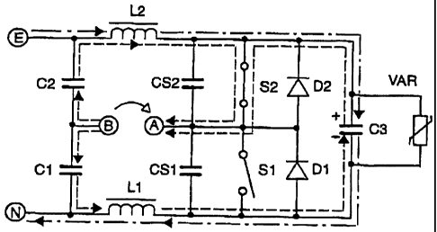
Such a half-bridge inverter known from the prior art
(see DE-A 197 22 124) is shown in Figure 1. A first and a
second input terminal E, N form an input, which has a storage
capacitor C3 connected in parallel with it. Connected in
parallel with the storage capacitor C3 is, on the one hand, a
varistor, i.e. a nonlinear resistor, as a surge arrester,
which ensures the necessary surge strength in practice, and
also the series circuit comprising a first and a second
coupling capacitor Cl, C2, the midpoint of said series
CA 02315445 2008-01-07
77332-71
la
circuit being connected to the first output terminal
B of the half-bridge inverter. In this arrangement,
the coupling capacitors Cl, C2 form the passive bridge
path of the half-bridge inverter. The active bridge
path of the half-bridge inverter, comprising a first
lp switch S1 and a second switch S2, is connected by its
midpoint to the second output terminal A of the half-
bridge inverter via an inductor Ll, the inductor Ll
acting as a polarity-reversal inductor. Connected in
parallel with the switches Sl and S2, which are
operated in push-pull mode, are a respective
freewheeling diode Dl, D2 and a respective polarity-
reversal capacitor CS1, CS2.
The first disadvantage of the half-bridge inverter
shown in Figure 1 is that, although the alternating
current flowing through C3 is filtered by C3, this is
not sufficient in practice, with the result that
unwanted perturbations are produced at the input E, N.
For the application instance where the circuit is
CA 02315445 2008-01-07
77332-71
2
designed to provide a high-frequency AC voltage on the
terminals B, A, problems arise with regard to radio
interference suppression. In addition, the inductor Ll
carries both the current load and the magnetization
load. This means that the inductor L1 needs to have
large dimensions,'which results in an undesirably high
space requirement.
The object of the present invention is therefore to
eliminate these disadvantages, and in particular to
provide a half-bridge inverter which can be produced
with a relatively small design.
The half-bridge inverter according to the invention
has the advantage that the current load and
magnetization load is split between two inductors. The
current load on each inductor Ll, L2 is therefore half
that of the current load on the inductor L1 shown in
Figure 1. The copper losses are thus now a quarter.
This allows relatively small components to be used for
production and thus reduces the space requirement on
a circuit board. Particularly for relatively high
powers, production is therefore greatly simplified. In
the case of the subject matter of the invention, the
storage capacitor C3 is advantageously no l'onger
arranged between the input terminals E, N, but instead
is virtually at the other end of the circuit. Assuming
that the half-bridge inverter has been designed for
high frequency, the high-frequency charge reversal
operations are thus as far away as possible from the
input terminals E, N, so that the perturbations of the
charge reversal operations in C3 have much less of an
influence on the input E, N than is the case in the
prior art. With particular advantage, the position of
the inductors Ll, L2 between C3 and the passive half-
bridge path comprising the coupling capacitors Cl, C2
increases the filter order by two orders, as seen from
CA 02315445 2000-08-10
3
the input E, N. This results in a significant
improvement in radio interference suppression and also
in an increase in the surge strength, provided that a
surge arrester is connected in parallel with C3. The
filter to be provided in a preliminary stage to the
left of the input E, N in Figure 2 can therefore be of
simpler design.
In addition, it should be pointed out that the
arrangement shown in Figure 1 - as seen from the input
terminals E, N - has only a first-order filter, since
all the capacitors and the surge arrester VAR
connected in parallel with the storage capacitor C3
are connected in parallel.
Provision may be made for the first switch to have a
first freewheeling diode connected in parallel with it
and for the second switch to have a second
freewheeling diode connected in parallel with it. In
addition, provision may be made for a first polarity-
reversal capacitor to be arranged in parallel with the
first switch and/or for a second polarity-reversal
capacitor to be arranged in parallel with the second
switch.
The optional surge arrester VAR may be in the form of
a nonlinear resistor, in particular in the form of a
varistor.
With particular advantage, the capacitance value of
the first coupling capacitor can be essentially the
same as the capacitance value of the second coupling
capacitor. The capacitance value of the storage
capacitor, which in the half-bridge inverter according
to the invention acts as a back-up capacitor for the
active bridge path, is preferably twice the
capacitance value of the first and/or of the second
coupling capacitor.
CA 02315445 2008-01-07
77332-71
4
In one particularly advantageous embodiment, the first
inductor is coupled to the second inductor. This
enables not just one variant to be produced, in which
the first and second inductors are wound on a single
core, but rather the coupling can also be designed to
be such that the principal inductances of the first
and second inductors cause the input current to be
smoothed, and that the leakage inductances of the
first and second inductors act as a polarity-reversal
inductance.
Illustrative embodiments of the half-bridge inverter
according to the invention are described in more
detail below with reference to the appended drawings,
in which:
Figure 1 shows a half-bridge inverter known from the
prior art;
Figure 2 shows a half-bridge inverter according to
the invention, where dash-dot lines show the
course of the direct current and dashed
lines show the course of the AC components.
Whereas Figure 2a shows the courses of
direct current and alternating current=when
the switch S2 is closed, Figure 2b shows
these courses when the switch S1 is closed;
and
Figure 3 shows an embodiment having'coupled inductors
L1, L2, with Figure 3a corresponding to
Figure 2a and Figure 3b corresponding to
Figure 2b in terms of the positions of the
switches SI and S2.
Unless indicated otherwise below, identical reference
CA 02315445 2000-08-10
symbols in the various figures denote identical
components. Figure 2a shows a first embodiment of a
half-bridge inverter according to the invention, where
the passive bridge path formed by the coupling
5 capacitors Cl, C2 is arranged in parallel with the
input terminals E, N. The midpoint of the passive
bridge path is connected to the output terminal B. The
active bridge path comprises two switches Si, S2
connected in series, their midpoint being connected to
the second output terminal A. Arranged in parallel
with each switch is a respective freewheeling diode
Dl, D2 and a respective polarity-reversal capacitor
CS1, CS2. A storage capacitor C3 is connected in
parallel with the active bridge path. In addition, an
optional surge arrester VAR is shown in Figure 2a. The
coupling capacitor C2 is connected to the switch S2
via an inductor L2, while the coupling capacitor Cl is
connected to the switch S1 via an inductor Ll. Dash-
dot lines show the course of the direct current from
the input terminal E via the inductor L2, the storage
capacitor C3 (for these deliberations, the resistance
of the surge arrester can be assumed to be infinite)
and the inductor L1 to the second input terminal N.
Dashed lines show the courses of the two AC
components, with the switch S2 being closed in
Figure 2a: a first AC component flows from the output
terminal B through the coupling capacitor C2 via the
inductor L2 through the switch S2 to the second output
terminal A. The second AC component flows from the
output terminal B via the coupling capacitor Cl,
through the inductor Li, the storage capacitor C3 and
the closed switch S2 to the second output terminal A.
Figure 2b shows the circumstances when the switch S1
is closed. As compared with Figure 2a, the course of
the direct current is unchanged. As regards the AC
components, a first one flows from the output terminal
A through the switch Si, through the inductor L1,
through the coupling capacitor Cl to the output
CA 02315445 2000-08-10
6
terminal B, while a second component flows from the
output terminal A, through the switch Si, the storage
capacitor C3, the inductor L2 and the coupling
capacitor C2 to the output terminal B. From the
current balance at C3, it follows that the storage
capacitor is charged by the direct current, while the
respective AC component discharges the storage
capacitor C3.
In series with the output terminals B, A, the parallel
circuit comprising the inductors Li, L2 acts as a
polarity-reversal inductance. The loading is thus
distributed between the two inductors Li and L2. The
inductors Li, L2, acting in series with the input
terminals E, N, cause the input current to be
effectively smoothed. In contrast to this, in the case
of the half-bridge inverter shown in Figure 1, AC
components are merely filtered out by the capacitor
C3.
Figures 3a and 3b show a further embodiment of the
half-bridge inverter according to the invention.
Figure 3a shows the courses of the direct current and
alternating current when the switch S2 is closed, and
Figure 3b shows them when the switch Sl is closed,
these switches corresponding to those in Figures 2a
and 2b. In contrast to the embodiments shown in
Figure 2a and Figure 2b, the two inductors Li, L2
shown in Figure 3a and Figure 3b are coupled to one
another. This significantly amplifies the smoothing
effect on the input current. The principal inductances
of the two inductors L1, L2 cause the input current to
be smoothed, while the leakage inductances of the two
inductors L1, L2 act as a polarity-reversal
inductance. It is possible to have an implementation
in which the two inductors Ll, L2 are wound on a
single core.
In contrast to the half-bridge inverter shown in
CA 02315445 2000-08-10
7
Figure 1, the filter order for the half-bridge
inverters according to the invention is increased by
two orders - as seen from the input E, N. This results
in a significant improvement in radio interference
suppression and also in an increase in the surge
strength, provided that a surge arrester VAR is
connected in parallel with the storage capacitor C3.