Note: Descriptions are shown in the official language in which they were submitted.
CA 02316177 2000-06-22
~-
- 1 -
SPECIFICATION
FRAME-SYNCHRONIZING-SIGNAL CAPTURING CIRCUIT OF
RECEIVER
Technical Field
The present invention relates to a
frame-synchronizing-signal capturing circuit of a receiver,
particularly to a frame-synchronizing-signal capturing
io circuit of a receiver for capturing a
frame-synchronizing-signal portion in two series of I and Q
symbol-stream data obtained by receiving and
demodulating a signal to be PSK-modulated in which a
BPSK-modulated frame-synchronizing signal or a
is BPSK-modulated frame-synchronizing signal and a
superframe-identifying signal, an 8PSK-modulated digital
signal, a QPSK-modulated digital signal, and a
BPSK-modulated digital signal are time-multiplexed in
accordance with a hierarchical transmission system or the
20 like.
Background Art
Practical use of digital satellite TV broadcast is
advanced which conforms to a plurality of modulation
25 systems having required C/Ns different from each other
CA 02316177 2000-06-22
- 2 -
such as hierarchical transmission systems in which a wave
to be 8PSK-modulated, a wave to be QPSK-modulated, and
a wave to be BPSK-modulated are time-multiplexed and
repeatedly transmitted every frame.
FIG. 7 is an illustration showing a frame configuration
of a hierarchical transmission system. One frame is
constituted of a frame-synchronizing-signal interval
comprising 32 BPSK-modulated symbols, a TMCC
(Transmission and Multiplexing Configuration Control)
signal interval comprising 128 BPSK-modulated symbols to
identify a transmission multiple configuration, a
superframe-identifying signal interval comprising 32
symbols, a main signal interval of 203
8PSK(trellis-coding-8PSK)-modulated symbols, a burst
symbol signal (BS) interval of four symbols in which a
pseudo random noise (PN) signal is BPSK-modulated, a
main signal interval of 203
8PSK(trellis-codec-8PSK) -modulated symbols, a burst
symbol signal (BS) interval of four symbols in which a
pseudo random noise (PN) signal is BPSK-modulated, ..., a
main signal interval of 203 QPSK-modulated symbols, a
burst symbol signal (BS) interval of four symbols in which
a pseudo random noise (PN) signal is BPSK-modulated, a
main signal interval of 203 QPSK-modulated symbols, and
CA 02316177 2000-06-22
- 3 -
a burst symbol signal (BS) interval of four BPSK-modulated
symbols in order.
FIG. 8 is an illustration showing a superframe
configuration according to the hierarchical transmission
system. One superframe is constituted of 8 consecutive
frames and a superframe-identifying signal serves as
information for identifying a superframe. The 192 symbols
from the head of a frame-synchronizing-signal interval up
to the end of a superframe-identifying-signal interval are
also referred to as a header.
The first-half 20 symbols of a
frame-synchronizing-signal interval of 32 symbols are
actually used as a frame-synchronizing signal. This is
because the first-half 20 symbols in a 32-symbol interval to
be originally used for another purpose serve as a unique
word and the unique word is used as a frame-synchronizing
signal. A frame-synchronizing signal comprising the 20
symbols is also referred to as "W 1" which is shown by the
following expression.
W 1=(SOS 1... S 18S 19)
=(11101100110100101000)
(This is transmitted from the SO side.)
Similarly, the first-half 20 symbols of a
superframe-identifying signal of 32 symbols are actually
used as a superframe-identifying signal. This is also
CA 02316177 2000-06-22
- 4 -
because the first-half 20 symbols of a 32-symbol interval to
be originally used for another purpose serve as a unique
word and the unique word is used as a
superframe-identifying signal. The first frame of a
superframe in the superframe-identifying signal comprising
20 symbols is also referred to as "W2" which is shown by
the following expression.
W2 = (UOU 1 ... U 18U 19)
=(00001011011001110111)
(This is transmitted from the U0 side.)
Frames other than the first frame of a superframe in a
superframe-identifying signal are also referred to as "W3"
which is obtained by inverting each bit of W2 and W3 is
shown by the following expression.
W3 = (VOV 1 ... V 18V 19)
=(11110100100110001000)
(This is transmitted from the VO side.)
Then, mapping for each modulation system at the
transmission side is described below by referring to FIGS.
9A to 9C. FIG. 9A shows signal point arrangements on I-Q
phase plane (also referred to as I-Q vector plane or I-Q
signal space diagram) when using 8PSK for a modulation
system. The 8PSK modulation system transmits a
three-bit digital signal (abc) by one symbol and
combinations of bits constituting one symbol include such
CA 02316177 2000-06-22
- 5 -
eight ways as (000), (001), (010), (011), (100), (101), (110),
and (111). These three-bit digital signals are converted
into signal point arrangements "0" to "7" on the
transmission-side I-Q phase plane in FIG. 9A and this
conversion is referred to as 8PSK mapping.
In case of the example shown in FIG. 9A, a bit string
(000) is converted into a signal point arrangement "0", a bit
string (001) into a signal point arrangement " 1", a bit string
(011) into a signal point arrangement "2," a bit string (010)
into a signal point arrangement "3", a bit string (100) into a
signal point arrangement "4", a bit string (101) into a
signal point arrangement "5", a bit string (111) into a
signal point arrangement "6", and a bit string (110) into a
signal point arrangement "7".
FIG. 9B shows signal point arrangements at I-Q phase
plane when using QPSK for a modulation system. The
QPSK modulation system transmits a two-bit digital signal
(de) by one symbol and combinations of bits constituting
the symbol include such four ways as (00), (01), (10), and
(11). In case of the example in FIG. 9B, a bit string (00) is
converted into a signal point arrangement "1," a bit string
(01) into a signal point arrangement "3", a bit string (11)
into a signal point arrangement "5", and a bit string (10)
into a signal point arrangement "7".
CA 02316177 2000-06-22
- 6 -
FIG. 9C shows signal point arrangements at the time
of using BPSK for a modulation system. The BPSK
modulation system transmits a one-bit digital signal (f) by
one symbol. In case of the digital signal (f), bit (0) is
converted into a signal point arrangement "0" and bit (1) is
converted into a signal point arrangement "4". Relations
between signal point arrangements and arrangement
numbers of various modulation systems are made same on
the basis of 8BPSK.
I-axis and Q-axis of each of QPSK and BPSK of the
hierarchical transmission system coincide with I-axis and
Q-axis of 8PSK.
In case of a receiver for receiving a digital wave to be
modulated (wave to be PSK-modulated) according to the
hierarchical transmission system, as shown in FIG. 10, an
intermediate-frequency signal IF of a signal received by a
not-illustrated receiving circuit is demodulated by a
demodulating circuit 1 and thus, I and Q base-band signals
(hereafter also referred to as I and Q symbol-stream data)
showing instantaneous values of I-axis and Q-axis
orthogonal to each other for each symbol are obtained.
When a frame-synchronizing signal is repeatedly captured
every certain frame cycle from the demodulated I and Q
base-band signals by a frame-sync detecting/regenerating
circuit 2, it is judged that frame sync is established and
CA 02316177 2000-06-22
- 7 -
thus, a frame-synchronizing pulse FSYNC is output or a
regenerated frame-synchronizing signal is output.
Furthermore, after establishing the frame sync, the
present rotation angle of the received signal can be
obtained from the signal points arrangement of the
frame-synchronizing part in the I, Q base-band signals
captured by a frame sync detecting/ regenerating circuit 2.
And, any desired absolute phasing corresponding to the
phase angle of a transmission signal can be established by
io reversely phase-rotating the I, Q base-band signals on the
basis of the obtained rotation angle of the received signal.
Moreover, after frame sync is established,
transmission-multiple-configuration identifying information
(refer to TMCC in FIG. 7) is separated and it is identified in
which modulation-system portion I and Q base-band
signals are included. In accordance with the identification
result, a main signal according to 8PSK modulation and a
main signal according to QPSK modulation are separated
from absolute-phase-generated I and Q base-band signals.
The demodulating circuit 1 orthogonally detects an
intermediate-frequency signal IF by using a regenerated
carrier wave and transmits I and Q base-band signals (also
referred to as I and Q symbol-stream data) 1(8) and Q(8)
(numeral in parentheses shows the number of quantization
bits and hereafter also referred to as I and Q by omitting
CA 02316177 2000-06-22
- 8 -
the number of quantization bits) of eight quantization bits
(two's complement system) showing instantaneous values of
I-axis and Q-axis for each symbol. The demodulating
circuit 1 according to the hierarchical transmission system
establishes frame sync and performs 8PSK demodulation
before a modulation system is identified. After frame sync
is established and a modulation system is identified, the
circuit 1 performs demodulation suitable for each
modulation system in accordance with the modulation
system of a received signal.
In the case of the demodulating circuit 1,
reception-side I- and Q-axes rotate by (7c/4)xn (n is one of
integers 0 to 7) against transmission-side I- and Q-axes
depending on a phase state of a regenerated carrier wave
for a received carrier wave and a phase of a received-signal
point on I-Q phase plane according to I and Q base-band
signals 1(8) and Q(8) at the reception side rotates when
receiving digital signals related to signal point
arrangements "0" to "7" on I-Q phase plane at the
transmission side. For example, bits (0) and (1) mapped to
signal point arrangements "0" and "4" at the transmission
side through BPSK mapping appear on signal point
arrangements "0" and "4" same as the transmission side
when a received-signal-phase rotation angle 0 at the
reception side is equal to 0.
CA 02316177 2000-06-22
- 9 -
However, transmission-side bits (0) and (1) appear on
signal point arrangements " 1" and "5" when a phase rotates
by 0=7c/4 at the reception side, appear on signal point
arrangements "2" and "6" when a phase rotates by 0=2n/4
at the reception side, appear on signal point arrangements
"3" and "7" when a phase rotates by 0=3n/4 at the reception
side, appear on signal point arrangements "4" and "0" when
a phase rotates by 0=4n/4 at the reception side, appear on
signal point arrangements "5" and " 1" when a phase rotates
by 0=57[/4 at the reception side, appear on signal point
arrangements "6" and "2" when a phase rotates by 0=67c/4
at the reception side, and appear on signal point
arrangements "7" and "3" when a phase rotates by 0=77c/ 4
at the reception side. The frame-sync
detecting/regenerating circuit 2 must correctly capture a
frame-synchronizing signal even if a regenerated carrier
wave of the demodulating circuit 1 has any phase state.
As shown in FIG. 10, the frame-sync
detecting/regenerating circuit 2 is constituted of a BPSK
demapper section 3, sync detecting circuits 40 to 47, an OR
gate circuit 53, a frame-synchronizing circuit 5, and a
frame-synchronizing-signal generator 6.
I and Q base-band signals 1(8) and Q(8) output from
the demodulating circuit 1 are input to the BPSK demapper
section 3 of the frame-sync detecting/regenerating circuit 2
CA 02316177 2000-06-22
- 10 -
in order to capture a frame-synchronizing signal and bit
streams BO to B7 BPSK-demapped are output for each of
eight received-signal-phase-rotation angles 0. The BPSK
demapper section 3 is constituted of, for example, a ROM.
In the hierarchical transmission system, a
frame-synchronizing signal is transmitted together with a
superframe-identifying signal by being BPSK-modulated so
as to minimize a required C/N. In the case of a bit stream
of a frame-synchronizing signal constituted of 20 bits, W 1
is equal to (SOS 1... S 18S 19)=(1 1 10 1 100 1 10 100 10 1000)
which are transmitted from SO in order. The bit stream is
converted to a signal point arrangement "0" or "4" through
the BPSK mapping shown in FIG. 9C at the transmission
side and a converted symbol stream is transmitted.
When a received-signal-phase rotation angle 0 is equal
to 0, bit (0) of a frame-synchronizing signal appears on a
signal point arrangement "0" and bit (1) of the signal
appears on a signal point arrangement "4" at the reception
side. To capture 20 bits, that is, a frame-synchronizing
signal of 20 symbols BPSK-modulated and transmitted, it is
necessary to convert received symbols into bit data through
the BPSK demapping shown in FIG. 12A inversely to
mapping converted at the transmission side. In FIG. 12A,
(0) is judged when a received-signal point shown by I and Q
base-band signals I and Q is kept in the right side of
CA 02316177 2000-06-22
- 11 -
Q-axis (positive side of I-axis; refer to the hatched portion)
on reception-side I-Q phase plane and (1) is judged when
the received-signal point is kept in the left side of Q-axis
(negative side of I-axis; refer to the unhatched portion).
That is, in FIG. 12A, an output is judged as (0) or (1)
depending on either of two judgement areas divided by a
BPSK criterion border line (coinciding with Q-axis) shown
by a bold line and thereby, it is judged that BPSK
demapping is performed.
I and Q base-band signals 1(8) and Q(8) are input to a
BPSK demapper 30 of the BPSK demapper section 3 shown
in FIG. 11 and the bit stream BO BPSK-demapped in FIG.
12A is output from the BPSK demapper 30. In this
specification, a demapper denotes a circuit for performing
demapping. The bit stream BO is input to the sync
detecting circuit 40 and a bit stream of a
frame-synchronizing signal is captured from the bit stream
BO in the sync detecting circuit 40.
Then, the sync detecting circuit 40 is described below
by referring to FIG. 14. The sync detecting circuit 40 has
20 D-flip-flops (hereafter referred to as D-F/Fs) D19 to DO
connected in series and a 20-stage shift register is
constituted of these D-F/Fs D19 to DO. The bit stream BO
is input to the D-F/F D19 and successively shifted up until
the D-F/F DO. At the same time, logical inversion is
CA 02316177 2000-06-22
- 12 -
applied to predetermined bits of the D-F/Fs D19 to DO and
then, outputs of the D-F/Fs D19 to DO are input to an AND
gate 51. An output SYNAO of the AND gate 51 becomes a
high potential when output states (DOD 1 ... D 18D 19) of the
D-F/Fs D19 to DO become (11101100110100101000).
That is, when W 1 is captured, SYNAO becomes a high
potential.
The output SYNAO of the sync detecting circuit 40 is
input to the frame-synchronizing circuit 5 through the OR
gate circuit 53. In the frame-synchronizing circuit 5, it is
judged that frame sync is established when it is confirmed
that a frame-synchronizing-signal capturing signal SYNA
output by the OR gate circuit 53 repeatedly becomes a high
potential every certain frame cycle and a
frame-synchronizing pulse FSYNC is output every frame
cycle.
A received-signal-phase rotation angle 0 may have an
angle other than 0. In this case, it is impossible to
capture a frame-synchronizing signal by a combination of
the BPSK demapper 30 and the sync detecting circuit 40.
As shown in FIG. 11, the BPSK demapper section 3 is
provided with BPSK demappers 31 to 37 corresponding to
received-signal-phase rotation angles 0=7r/4, 2n/4, 3n/4,
47z/4, 57c/4, 67c/4, and 77c/4.
CA 02316177 2000-06-22
- 13 -
FIG. 12B shows BPSK demapping when a symbol
stream of a demodulated frame-synchronizing signal is
phase-rotated by 0=7c/4 and bit (0) appears on a signal
point arrangement " 1" and bit (1) appears on a signal point
arrangement "5". In FIG. 12B, a BPSK criterion border
line shown by a bold line rotates by Tc/4 counterclockwise
from the basic BPSK criterion border line of BPSK
demapping shown by a bold line in FIG. 12A in the case of
reception at the same phase as that of the transmission
side. The BPSK demapper 31 performs BPSK demapping in
accordance with FIG. 12B. In FIG. 12B, (0) is judged when
a received-signal point shown by I and Q base-band signals
I and Q is kept in the top right area of the BPSK criterion
border line and (1) is judged when the received-signal point
is kept in the left bottom area of the border line. A bit
stream BPSK-demapped by the BPSK demapper 31 serves
as an output B 1 of the BPSK demapper section 3 in FIG.
10.
Similarly, the BPSK demappers 32 to 37 perform BPSK
demapping at BPSK criterion border lines rotated by 2n/4,
3n/4, ..., and 7n/4 counterclockwise from the basic BPSK
criterion border line shown by a bold line of the BPSK
demapping in FIG. 12A (refer to FIGS. 12C and 12D and
FIGS. 13A to 13D) to stably capture frame-synchronizing
signals phase-rotated by 0=27c/4, 3n/4, ..., and 77c/4
CA 02316177 2000-06-22
- 14 -
against the transmission side. Bit streams
BPSK-demapped by the BPSK demappers 32 to 37 serve as
outputs B2 to B7 of the BPSK demapper section 3 in FIG.
10.
Configurations of the sync detecting circuits 41 to 47
are the same as the configuration of the sync detecting
circuit 40. By using these sync detecting circuits 40 to 47,
a frame-synchronizing signal is captured in accordance
with a combination of any BPSK demapper and any sync
detecting circuit independently of phase rotation of a
base-band signal against the transmission side according
to a phase state of a regenerated carrier wave in the
demodulating circuit 1 and a high-potential signal SYNAn
(n is one of integers 0 to 7) is transmitted from a sync
detecting circuit of a system capturing a
frame-synchronizing signal.
Signals SYNAn output from the sync detecting circuits
40 to 47 are input to the OR gate circuit 53 in which the
logical sum is computed. When any signal SYNAn becomes
a high potential, a high-potential
frame-synchronizing-signal capturing signal SYNA showing
that a frame-synchronizing signal is captured is output
from the OR gate circuit 53. The frame-synchronizing
circuit 5 judges that frame sync is established when it is
confirmed that a high potential of SYNA is repeatedly input
CA 02316177 2000-06-22
- 15 -
every certain frame interval and outputs a
frame-synchronizing pulse FSYNC every frame cycle.
Whenever receiving the frame-synchronizing pulse FSYNC
from the frame-synchronizing circuit 5, the
frame-synchronizing-signal generator 6 generates a bit
stream (referred to as a regenerated frame-synchronizing
signal) same as a bit pattern W 1 of a frame-synchronizing
signal captured by the BPSK demapper section 3 and the
sync detecting circuits 40 to 47.
The process is described above in which a
frame-synchronizing signal is captured from I and Q
base-band signals 1(8) and Q(8) output from the
demodulating circuit 1 by the frame-sync
detecting/regenerating circuit 2 shown in FIG. 10 and a
frame-synchronizing pulse FSYNC is output after a certain
time and a regenerated frame-synchronizing signal is
output.
When frame sync is established, processings such as
identification of a transmission multiple configuration,
detection of a received-signal-phase rotation angle, and
absolute phase generation for making a received-signal
phase coincide with that of the transmission side are
performed. For example, an operation for identifying each
transmission configuration by a not-illustrated
transmission-configuration identifying circuit is performed
CA 02316177 2000-06-22
- 16 -
as described below. When a frame-synchronizing pulse
FSYNC is output, the transmission-configuration
identifying circuit captures a bit stream Bn of a system
repeatedly becoming a high potential among SYNAO to
SYNA7, extracts the TMCC pattern in FIG. 9 by using a
predetermined timing signal generated from the
frame-synchronizing pulse FSYNC, decodes the TMCC
pattern, and outputs a modulation-system identifying
signal showing on which modulation system the present I
and Q base-band signals I and Q depend to the
demodulating circuit 1 and the like. The demodulating
circuit 1 performs demodulation suitable for a modulation
system of a received signal in accordance with an input
modulation-system identifying signal.
1s However, under the worst receiving environment in
which a received C/N becomes 0 dB, a transmission error
rate of the BPSK modulation system becomes approx. 10-1.
Therefore, an error occurs in approx. 2 bits of a
frame-synchronizing signal comprising 20 symbols. In this
case, a problem occurs in the above-described conventional
frame-sync detecting/regenerating circuit 2 that none of
the sync detecting circuits 40 to 47 can capture a
frame-synchronizing signal, thus frame sync cannot be
established, and no digital signal can be received. To
solve the problem, if each of the sync detecting circuits 40
CA 02316177 2000-06-22
- 17 -
to 47 outputs a frame-synchronizing signal by allowing an
error of approx. several bits, a true frame-synchronizing
signal cannot be captured because many patterns similar
to a symbol pattern of the frame-synchronizing signal
appear in I and Q symbol streams.
It is an object of the present invention to provide a
frame-synchronizing-signal capturing circuit of a receiver
capable of stably capturing frame-synchronizing signals
even under the worst receiving environment.
Disclosure of the Invention
The frame-synchronizing-signal capturing circuit of a
receiver according to claim 1 of the present invention for
capturing a frame-synchronizing signal from I and Q
symbol-stream data obtained by receiving and
demodulating a signal to be PSK-modulated in which
BPSK-modulated frarne-synchronizing signal and
superframe-identifying signal, an 8PSK-modulated digital
signal, a QPSK-modulated digital signal, and a
BPSK-modulated digital signal are time-multiplexed,
comprises BPSK demapping means for independently
BPSK-demapping I and Q symbol-stream data in
accordance with four criterion border lines obtained by
rotating a criterion border line for performing
BPSK-demapping to bits (0) and (1) (or (1) and (0))
CA 02316177 2000-06-22
- 18 -
depending on the fact that a received-signal point
according to I and Q symbol-stream data is present at right
side or left side of Q-axis on I-Q phase plane by (7c/4)xm (m
denotes four integers selected out of integers 0 to 7 so that
the four integers are not duplicated and a selected angle
does not coincide with others even if it is rotated by 7c) and
outputting bit streams of four systems; first comparing
means provided for each system of outputs of the BPSK
demapping means to compare a data pattern held by a shift
register with a frame-synchronizing-signal pattern or an
inverted-frame-synchronizing-signal pattern while inputting
a bit stream to the shift register and perform
correlation-detection output when there are matched
numbers in bit unit equal to or more than a predetermined
first specified value P and there are only matched numbers
equal to or less than a predetermined second specified
value R; second comparing means provided for each system
output from the BPSK demapping means to compare a data
pattern held by a shift register with a
superframe-identifying-signal pattern or an
inverted-superframe-identifying-signal pattern while
inputting a bit stream to the shift register and perform
correlation-detection output when there are matched
numbers in bit unit equal to or more than a predetermined
third specified value P' and there are only matched
CA 02316177 2000-06-22
- 19 -
numbers in bit unit equal to or less than a predetermined
fourth specified value R'; and frame-synchronizing-signal
capturing-signal generating means for outputting a
frame-synchronizing-signal capturing signal when a
correlation-detection output supplied from one of the first
comparing means and a correlation-detection output
supplied from one of the second comparing means are
generated in accordance with a predetermined temporal
relation.
The BPSK demapping means independently
BPSK-demaps I and Q symbol-stream data in accordance
with four criterion border lines obtained by rotating a basic
criterion border line for performing BPSK-demapping to bits
(0) and (1) (or (1) and (0)) depending on the fact that a
1s received-signal point according to I and Q symbol-stream
data is present at right side (positive side of I-axis) or left
side (negative side of I-axis) of Q-axis on I-Q phase plane
by (7c/4)xm (m denotes four integers selected out of integers
0 to 7 so that the four integers are not duplicated and a
selected angle does not coincide with others even if it is
rotated by 7t) and outputs bit streams of four systems.
When assuming that rotation angles of four criterion border
lines against the basic criterion border line are equal to 0,
to 04, symbol streams received at received-signal-phase
rotation angles 0=01 and O i+zc are changed to bit streams
CA 02316177 2000-06-22
- 20 -
through the demapping using a criterion border line of 01
(however, in the case of O 1+7r, a bit stream is obtained in
which bits (0) and (1) are inverted). A symbol stream is
changed to a bit stream in the case when a
received-signal-phase rotation angle 0 is equal to 0, 7c/4,
2n/4, 37c/4, 47r/4, 57c/4, 67c/4, or 7n/4 in combination with
the demapping using criterion border lines of 02 to 04.
The first comparing means for inputting a bit stream
demapped at a criterion border line of Oi (i is one of
integers 1 to 4) by assuming a bit length of a
frame-synchronizing signal as FL performs correction
detection output when a frame-synchronizing-signal
pattern is an object to be compared, a
received-signal-phase rotation angle 8 is equal to Oi, and a
pattern having only a difference within (FL-P) bits from a
frame-synchronizing signal appears in the bit stream and
performs correlation-detection output by assuming that a
pattern having only a difference within R bits from the
frame-synchronizing signal unless inverted appears when a
pattern matched with the frame-synchronizing signal only
within R bits appears in a bit stream inverted against the
transmission side and a received-signal-phase rotation
angle 0 is equal to 0;+7c (moreover, when an inverted
frame-synchronizing-signal pattern is an object to be
compared, a received-signal-phase rotation angle 0 is equal
CA 02316177 2000-06-22
- 21 -
to O;, and a pattern matched with an inverted
frame-synchronizing signal within only R bits appears in a
bit stream, the first comparing means performs
correlation-detection output by assuming that a pattern
having only a difference within R bits from a
frame-synchronizing signal appears and when a
received-signal-phase rotation angle 0 is equal to O; and a
pattern having only a difference within only (FL-P) bits
from an inverted frame-synchronizing signal appears in a
bit stream inverted against the transmission side, the first
comparing means performs correlation-detection output by
assuming that a pattern having only a difference within
(FL-P) bits from the frame-synchronizing signal unless
inverted appears).
Moreover, the second comparing means for inputting a
bit stream demapped at a criterion border line of O; (i is
one of integers 1 to 4) by assuming a bit length of a
superframe-identifying signal as SFL performs correction
detection output when a superframe-identifying-signal
pattern is an object to be compared, a
received-signal-phase rotation angle 0 is equal to Oi, and a
pattern having only a difference within (SFL-P') bits from a
superframe-identifying signal appears in the bit stream and
performs correlation-detection output by assuming that a
pattern having only a difference within R' bits from the
CA 02316177 2000-06-22
- 22 -
superframe-identifying signal unless inverted appears when
a pattern matched with the frame-synchronizing signal only
within R' bits appears in a bit stream inverted against the
transmission side and a received-signal-phase rotation
angle 6 is equal to Oi+7E (moreover, when an inverted
superframe-identifying-signal pattern is an object to be
compared, a received-signal-phase rotation angle 6 is equal
to O;, and a pattern matched with an inverted
superframe-identifying signal within only R' bits appears in
a bit stream, the second comparing means performs
correlation-detection output by assuming that a pattern
having only a difference within R' bits from a
superframe-identifying signal unless inverted appears and
moreover, when a received-signal-phase rotation angle 6 is
equal to O;+n and a pattern having only a difference within
only (SFL-P') bits from an inverted superframe-identifying
signal appears in a bit stream inverted against the
transmission side, the second comparing means performs
correlation-detection output by assuming that a pattern
having only a difference within (SFL-P') bits from the
superframe-identifying signal unless inverted appears).
The frame- synchronizing- signal capturing- signal
generating means outputs a frame-synchronizing-signal
capturing signal when correlation-detection output from
one of the first comparing means and correlation-detection
CA 02316177 2000-06-22
- 23 -
output from one of the second comparing means are
generated in accordance with a predetermined time
relation.
In the case of the hierarchical transmission system, a
frame-synchronizing signal and a superframe-identifying
signal are arranged in one frame in accordance with a
predetermined positional relation. When a pattern having
a difference of only one bit to several bits from a pattern of
a frame-synchronizing signal and a pattern having a
difference of only one bit to several bits from the pattern of
the frame-synchronizing signal appear in demodulated I
and Q symbol-stream data in accordance with a
predetermined time relation specified by a frame format,
the pattern having a difference of only one bit to several
is bits from the pattern of the frame-synchronizing signal has
a very high possibility that the pattern is a
frame- synchronizing signal. Therefore, when
correlation-detection output from one of the first comparing
means and correlation-detection output from one of the
second comparing means are generated in accordance with
a predetermined time relation, it is possible to stably
capture frame-synchronizing signals by outputting a
frame-synchronizing-signal capturing signal and therefore,
reception is not made impossible.
CA 02316177 2000-06-22
- 24 -
The frame-synchronizing-signal capturing circuit of a
receiver according to claim 2 of the present invention
comprises BPSK demapping means for independently
BPSK-demapping I and Q symbol-stream data in
accordance with four criterion border lines obtained by
rotating a criterion border line for performing
BPSK-demapping to bits (0) and (1) (or (1) and (0))
depending on the fact that a received-signal point
according to I and Q symbol-stream data is present at right
side or left side of Q-axis on I-Q phase plane by (7t/4)xm (m
denotes four integers selected out of integers 0 to 7 so that
the four integers are not duplicated and a selected angle
does not coincide with others even if it is rotated by n) and
outputting bit streams of four systems; comparing means
ls provided for each system of outputs of the BPSK demapping
means to compare a data pattern held by a shift register
with a frame-synchronizing-signal pattern or an
inverted-frame-synchronizing-signal pattern while inputting
a bit stream to the shift register and perform
correlation-detection output when there are matched
numbers in bit unit equal to or more than a predetermined
first specified value P and there are only matched numbers
equal to or less than a predetermined second specified
value R; and frame-synchronizing-signal-capturing-signal
generating means for outputting a
CA 02316177 2000-06-22
- 25 -
frame-synchronizing-signal capturing signal when
correlation-detection output is generated from one of
comparing means and thereafter, correlation-detection
output is generated again from one of the comparing means
again at a timing when elapsing by a predetermined time.
In the case of the hierarchical transmission system, a
frame-synchronizing signal is set to a predetermined
position in one frame. When a pattern having a difference
of only one bit to several bits from a pattern of the
frame-synchronizing signal appears in demodulated I and Q
symbol-stream data every frame cycle, the pattern having a
difference of only one bit to several bits from the pattern of
the frame-synchronizing signal has a very high possibility
that it is a frame-synchronizing signal. Therefore, when
correlation-detection output is generated from one of
comparing means and thereafter, correction detection
output is generated again from one of the comparing means
at a timing when elapsing by a predetermined time such as
one frame cycle or two frame cycles, it is possible to stably
capture frame-synchronizing signals by outputting a
frame-synchronizing-signal capturing signal and therefore,
reception is not made impossible.
The frame-synchronizing-signal capturing circuit of a
receiver according to claim 3 of the present invention
comprises BPSK demapping means for independently
CA 02316177 2000-06-22
- 26 -
BPSK-demapping I and Q symbol-stream data to output bit
streams of four systems in accordance with four criterion
border lines obtained by rotating a criterion border line for
performing BPSK-demapping to bits (0) and (1) (or (1) and
(0)) depending on the fact that a received-signal point
according to I and Q symbol-stream data is present at right
side or left side of Q-axis on I-Q phase plane by (Tc/4)xm (m
denotes four integers selected out of integers 0 to 7 so that
the four integers are not duplicated and a selected angle
does not coincide with others even if it is rotated by 7t);
comparing means provided for each system of outputs of
the BPSK demapping means to compare a data pattern held
by a shift register with a superframe-identifying-signal
pattern or an inverted-superframe-identifying-signal
pattern while inputting a bit stream to the shift register
and perform correlation-detection output when there are
matched numbers in bit unit equal to or more than a
predetermined specified value P' and there are only
matched numbers equal to or less than a predetermined
specified value R'; and
frame-synchronizing-signal-capturing-signal generating
means for outputting a temporary
frame-synchronizing-signal capturing signal when a
correlation-detection output is generated from one of the
comparing means and thereafter, a correlation-detection
CA 02316177 2000-06-22
- 27 -
output is generated again from one of the comparing means
at a timing when elapsing by a predetermined time.
In the case of the hierarchical transmission system, a
frame-synchronizing signal and a superframe-identifying
signal are set to predetermined positions in one frame.
When a pattern having a difference of only one bit to
several bits from a pattern of the superframe-identifying
signal appears in demodulated I and Q symbol-stream data
every frame cycle, the pattern having a difference of only
io one bit to several bits from the pattern of the
superframe-identifying signal has a very high possibility
that it is a superframe-synchronizing signal and a
posisibility that a frame-synchronizing signal appears in
accordance with a certain time relation is very high.
Therefore, when correlation-detection output is generated
from one of the comparing means and thereafter,
correlation-detection output is generated again from one of
the comparing means at a timing when elapsing by a
predetermined time such as one frame cycle, two frame
cycles, or one superframe cycle, it is possible to stably
capture frame-synchronizing signals by outputting a
temporary frame-synchronizing-signal capturing signal and
therefore, reception is not disabled.
Brief Description of the Drawings
CA 02316177 2000-06-22
- 28 -
FIG. 1 is a block diagram of a configuration of an
essential portion of the wave-to-be-PSK-modulated receiver
of an embodiment of the present invention;
FIG. 2 is a block diagram showing a configuration of a
first comparing circuit in FIG. 1;
FIG. 3 is an illustration showing outputs and inputs of
a matched-number measuring circuit in FIG. 2;
FIG. 4 is a block diagram showing a configuration of a
second comparing circuit in FIG. 1;
FIG. 5 is a block diagram showing an essential portion
of the wave-to-be-PSK-modulated receiver of a modification
of the embodiment in FIG. 1;
FIG. 6 is a block diagram showing an essential portion
of the wave-to-be-PSK-modulated receiver of another
modification of the embodiment in FIG. 1;
FIG. 7 is an illustration showing a frame configuration
of a hierarchical transmission system;
FIG. 8 is an illustration showing a superframe
configuration of a hierarchical transmission system;
FIGS. 9A to 9C are illustrations showing signal point
arrangements for PSK mapping;
FIG. 10 is a block diagram showing a configuration
around a demodulating circuit of a
wave-to-be-PSK-modulated receiver according to a
conventional hierarchical transmission system;
CA 02316177 2000-06-22
- 29 -
FIG. 11 is a block diagram showing a configuration of
a BPSK demapper section in FIG. 10;
FIGS. 12A to 12D are illustrations for explaining BPSK
demapping;
FIGS. 13A to 13D are illustrations for explaining BPSK
demapping; and
FIG. 14 is a circuit diagram showing a configuration of
a sync detecting circuit in FIG. 10.
Best Mode for Carrying Out the Invention
Then, an embodiment of the present invention is
described below by referring to FIG. 1.
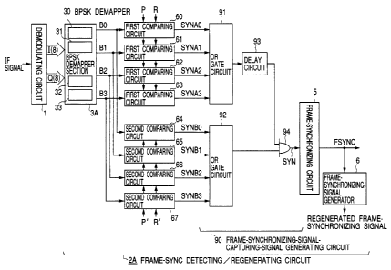
FIG. 1 is a block diagram of an essential portion of a
wave-to-be-PSK-modulated receiver of the present invention,
Zs in which a component same as those in FIGS. 10 and 11 is
provided with the same symbol.
I and Q base-band signals 1(8) and Q(8) output from a
demodulating circuit 1 are input to a BPSK demapper
section 3A of a frame-sync detecting/regenerating circuit
2A in order to capture a frame synchronizing signal and bit
streams BO to B3 are output which are BPSK-demapped for
each of four sets obtained by combining every two
received-signal-phase rotation angles out of eight
received-signal-phase rotation angles 0 such as 0, 7c/4,
27c/4, 37c/4, 47c/4, 57c/4, 67c/4, and 77c/4 so that every two
CA 02316177 2000-06-22
- 30 -
received-signal-phase rotation angles are different from
each other by 7t. The BPSK demapper section 3A is
constituted of, for example, a ROM.
The BPSK demapper section 3A has four BPSK
demappers 30 to 33 (for the BPSK demappers 30 to 33,
refer to FIG. 11). Each of the BPSK demappers 30 to 33
independently BPSK-demaps I and Q symbol-stream data
1(8) and Q(8) to output bit streams BO to B3 of four systems
in accordance with four BPSK criterion border lines
obtained by rotating a basic BPSK criterion border line
(refer to the bold line in FIG. 12A) for performing
BPSK-demapping to bits (0) and (1) (or (1) and (0))
depending on the fact that a received-signal point
according to I and Q symbol-stream data 1(8) and Q(8) is
ls present at right side (positive side of I-axis) or left side
(negative side of I-axis) of Q-axis on I-Q phase plane by
(0=n/4)xm (m denotes four integers selected out of integers
0 to 7 so that the four integers are not duplicated and a
selected angle does not coincide with others even if it is
rotated by n).
Specifically, the BPSK demapper 30 is used to
correctly BPSK-demap a received symbol stream when a
received-signal-phase rotation angle 0 is equal to 0 or n,
which performs demapping to bit (0) or (1) depending on
the fact that a received-signal point according to I and Q
CA 02316177 2000-06-22
- 31 -
symbol-stream data 1(8) and Q(8) is present at right side or
left side of a basic BPSK criterion border line (coinciding
with Q-axis) on I-Q phase plane in accordance with the
basic BPSK criterion border line shown in FIG. 12A when
m=O (01=0) is selected. When the received-signal-phase
rotation angle 0 is equal to 0, a bit stream same as that of
the transmission side is output. However, when 0 is equal
to 7c, a bit stream in which bits (0) and (1) are inverted is
output to the transmission side.
Moreover, the BPSK demapper 31 is used to correctly
BPSK-demap a received symbol stream when a
received-signal-phase rotation angle 0 is equal to 7c/4 or
57c/4, which performs demapping to bit (0) or (1) depending
on the fact that a received-signal point according to I and Q
symbol-stream data 1(8) and Q(8) is present at top right
side or bottom left side of a BPSK criterion border line on
I-Q phase plane in accordance with the BPSK criterion
border line (refer to FIG. 12B) obtained by rotating the
basic BPSK criterion border line shown in FIG. 12A
counterclockwise by n/4 when m=1 (02=n/4) is selected.
When the received-signal-phase rotation angle 0 is equal to
n/4, a bit stream same as that of the transmission side is
output. However, when the 0 is equal to 5n/4, a bit
stream in which bits (0) and (1) are inverted is output to
the transmission side.
CA 02316177 2000-06-22
- 32 -
The BPSK demapper 32 is used to correctly
BPSK-demap a received symbol stream when a
received-signal-phase rotation angle 0 is equal to 27c/4 or
67c/4, which performs demapping to bit (0) or (1) depending
on the fact that a received-signal point according to I and Q
symbol-stream data 1(8) and Q(8) is present at upper side
or lower side of a BPSK criterion border line on I-Q phase
plane in accordance with a BPSK criterion border line
obtained by rotating the basic BPSK criterion border line
shown in FIG. 12A counterclockwise by 27c/4 (refer to FIG.
12C) when m=2 (03=2n/4) is selected. However, when the
received-signal-phase rotation angle 0 is equal to 27c/4, a
bit stream same as that of the transmission side is output.
However, when the 0 is equal to 67c/4, a bit stream in which
bits (0) and (1) are inverted is output to the transmission
side.
The BPSK demapper 33 is used to correctly
BPSK-demap a received symbol stream when a
received-signal-phase rotation angle 0 is equal to 37c/4 or
7n/4, which performs demapping to bit (0) or (1) depending
on the fact that a received-signal point according to I and Q
symbol-stream data 1(8) and Q(8) is present at top left side
or bottom right side of a BPSK criterion border line on I-Q
phase plane in accordance with a BPSK criterion border
line obtained by rotating the basic BPSK criterion border
CA 02316177 2000-06-22
- 33 -
line shown in FIG. 12A counterclockwise by 3n/4 (refer to
FIG. 12D) when m=3 (CO4=37E/4) is selected. When the
received-signal-phase rotation angle 0 is equal to 3n/4, a
bit stream same as that of the transmission side is output.
However, when the 0 is equal to 7n/4, a bit stream in which
bits (0) and (1) are inverted is output to the transmission
side.
First comparing circuits 60 to 63 and second
comparing circuits 64 to 67 are provided for output sides of
the BPSK demappers 30 to 33. The first comparing
circuits 60 to 63 have the same configuration and the
configuration of the first comparing circuit 60 is shown in
FIG. 2. The first comparing circuit 60 has 20 D-flip-flops
(hereafter referred to as D-F/Fs) D19 to DO connected in
series and a 20-stage shift register is constituted of these
D-F/Fs D19 to DO. A bit stream BO is input to the D-F/F
D19 and successively shift up until the D-F/F DO. Data
R19 to RO held by (stored in) the D-F/Fs D19 to DO are
input to one input terminals of 20 EX-NOR circuits EX19 to
EXO individually set. Bit data S19 to SO constituting a bit
stream pattern W 1 of a frame-synchronizing signal are
input to the other input terminals of the EX-NOR circuits
EX 19 to EXO.
Outputs XO to X19 of the EX-NOR circuits EXO to
EX19 are set to (1) when two inputs are matched and to (0)
CA 02316177 2000-06-22
- 34 -
when two inputs are not matched. Five matched-number
measuring circuits 70 to 74 are provided for output sides of
the EX-NOR circuits EXO to EX19, in which each of the
circuits 70 to 74 is connected to every four of the circuits
EXO to EX19. The matched-number measuring circuits 70
to 74 measure the input number of (1)s and output
measured matched-number data NDO to ND4. For example,
the matched-number measuring circuit 70 outputs NDO
according to the relation in FIG. 3 correspondingly to
states of X0 to X3 input from the EX-NOR circuits EXO to
EX3. The same is true for other matched-number
measuring circuits 71 to 74. It is possible to simply
constitute these matched-number measuring circuits 70 to
74 in small size in accordance with table conversion by a
ROM or a combinational logic circuit.
Outputs NDO to ND4 of the matched-number
measuring circuits 70 to 74 are added by an adder 75 and
an added value is input to a comparing and judging circuit
76 as ND. The comparing and judging circuit 76 outputs a
high-potential correlation-detecting signal SYNAO when ND
is equal to or larger than a predetermined first specified
value P or ND is equal to or smaller than a predetermined
second specified value R. In this case, it is assumed that
P is set to 18 and R is set to 2.
CA 02316177 2000-06-22
- 35 -
Then, operations of the BPSK demapper 30 and first
comparing circuit 60 are described below. When a
received-signal-phase rotation angle 0 is equal to 0 and the
portion of a BPSK-modulated frame-synchronizing signal
W 1 is correctly received, a bit stream BO which is the
portion of the frame-synchronizing signal W 1 and in which
(0) or (1) is not inverted is output from the BPSK demapper
30. In this case, when a frame-synchronizing-signal
portion is just held by the D-F/Fs DO to D19 constituting a
shift register of the first comparing circuit 60 and output
states (ROR1 ... R18R19) become (11101100110100101000),
outputs NDO to ND5 of the matched-number measuring
circuits 70 to 74 become 4 and an output ND of the adder
75 becomes 20. In this case, the comparing and judging
circuit 76 shows ND_P and has a difference of (20-P) bits or
less from a bit pattern W 1. Therefore, the circuit 76
outputs a high-potential correlation-detecting signal SYNAO
(the high-potential correlation-detecting signal SYNAO
shows a possibility of capturing a frame-synchronizing
signal).
When a received-signal-phase rotation angle 0 is equal
to 0 and a receiving environment is deteriorated, an error
of 1 bit or 2 bits occurs in a bit stream BO of a
frame-synchronizing-signal portion transmitted from the
BPSK demapper 30. In this case, when the
CA 02316177 2000-06-22
- 36 -
frame-synchronizing-signal portion is just held by the
D-F/Fs DO to D19, an output ND of the adder 75 is equal
to 18 or 19 and the comparing and judging circuit 76
shows ND_P. Therefore, the circuit 76 outputs a
high-potential correlation-detecting signal SYNAO showing
a possibility of capturing a frame-synchronizing signal.
However, also when a pattern having only a difference of
approx. 2 bits from a frame-synchronizing signal is present
at a 20-bit portion of the bit stream BO other than the
lo frame-synchronizing signal, the comparing and judging
circuit 76 outputs a high-potential correlation-detecting
signal SYNAO. Therefore, it is not judged that a
frame-synchronizing signal is captured even if only an
expression ND_P is effectuated.
When a received-signal-phase rotation angle 0 is equal
to n and a BPSK-modulated frame-synchronizing signal is
correctly received, a bit stream BO which is the portion of a
frame-synchronizing signal (W1) and in which (0) and(1) are
inverted is output from the BPSK demapper 30. In this
case, when output states (ROR1 ... R18R19) of the D-F/F
DO to D19 of the first comparing circuit 60 become
(00010011001011010111) obtained by inverting a bit
pattern of a frame-synchronizing signal, outputs NDO to
ND5 of the matched-number measuring circuits 70 to 74
become 0 and an output ND of the adder 75 becomes 0. In
CA 02316177 2000-06-22
- 37 -
this case, the comparing and judging circuit 76 shows
ND<_R that is matched with W 1 in (20-R) bits or more
unless inverted. Therefore, the circuit 76 outputs a
high-potential correlation-detecting signal SYNAO showing
a possibility of capturing a frame-synchronizing signal.
When a received-signal-phase rotation angle 0 is equal
to 7c and a receiving environment is deteriorated, an error of
1 bit or 2 bits occurs in a bit stream BO in which a
frame-synchronizing-signal portion transmitted from the
BPSK demapper 30 is inverted. In this case, when an
inverted pattern of the frame-synchronizing-signal portion
is just held by the D-F/F DO to D19, an output ND of the
adder 75 is equal to 1 to 2 and the comparing and judging
circuit 76 shows ND<_R. Therefore, the circuit 76 outputs
a high-potential correlation-detecting signal SYNAO
showing a possibility of capturing a frame-synchronizing
signal. Moreover, when a pattern having a difference of
only approx. 2 bits from an inverted frame-synchronizing
signal is occasionally present at a 20-bit portion of a bit
stream BO other than the inverted frame-synchronizing
signal, the comparing and judging circuit 76 also outputs a
high-potential correlation-detecting signal SYNAO.
Therefore, it is not judged that a frame-synchronizing
signal is captured even if only an expression ND<_R is
effectuated.
CA 02316177 2000-06-22
- 38 -
The first comparing circuits 6 1 to 63 are constituted
completely the same as the first comparing circuit 60 is.
When a received-signal-phase rotation angle 0 is equal to
n/4 and a BPSK-modulated frame-synchronizing signal is
received, a non-inverted bit stream of a
frame-synchronizing-signal portion is output from the
BPSK demapper 31. When a received-signal-phase rotation
angle 0 is equal to 5n/4 and a BPSK-modulated
frame-synchronizing signal is received, an inverted bit
io stream of a frame-synchronizing-signal portion is output
from the BPSK demapper 31. Similarly to the case of the
first comparing circuit 60, when a frame-synchronizing
signal is correctly received or a receiving environment is
deteriorated and an error of 1 bit or 2 bits is received, the
first comparing circuit 61 outputs a high-potential
correlation-detecting signal SYNA 1 showing a possibility of
capturing a frame-synchronizing signal.
When a received-signal-phase rotation angle 0 is equal
to 27c/4 and a BPSK-modulated frame-synchronizing signal
is received, a non-inverted bit stream of a
frame-synchronizing-signal portion is output from the
BPSK demapper 32. When a received-signal-phase rotation
angle 0 is equal to 6n/4 and a BPSK-modulated
frame-synchronizing signal is received, an inverted bit
stream of a frame-synchronizing-signal portion is output
CA 02316177 2000-06-22
- 39 -
from the BPSK demapper 32. When a frame-synchronizing
signal is correctly received or a receiving environment is
deteriorated and a frame-synchronizing signal is received
with an error of 1 bit or 2 bits, the first comparing circuit
62 outputs a high-potential correlation-detecting signal
SYNA2 showing a possibility of capturing a
frame-synchronizing signal.
When a received-signal-phase rotation angle 0 is equal
to 37c/4 and a BPSK-modulated frame-synchronizing signal
is received, a non-inverted bit stream of a
frame-synchronizing-signal portion is output from the
BPSK demapper 33. When a received-signal-phase rotation
angle 0 is equal to 77c/4 and a BPSK-modulated
frame-synchronizing signal is received, an inverted bit
stream of a frame-synchronizing-signal portion is output
from the BPSK demapper 33. When a frame-synchronizing
signal is correctly received or a receiving environment is
deteriorated and a frame-synchronizing signal is received
with an error of 1 bit or 2 bits, the first comparing circuit
63 outputs a high-potential correlation-detecting signal
SYNA3 showing a possibility of capturing a
frame-synchronizing signal.
The second comparing circuits 64 to 67 have the same
configuration. FIG. 4 shows a configuration of the second
comparing circuit 64. The second comparing circuit 64
CA 02316177 2000-06-22
- 40 -
has 20 D-flip-flops (hereafter referred to as D-F/Fs) D19' to
DO' connected in series. A 20-stage shift register is
constituted of these D-F/Fs D19' to DO'. A bit stream BO
is input to the D-F/F D19' and successively shifted up
until the D-F/F DO'. Data R19' to RO' held by (stored in)
the D-F/Fs D19' to DO' are input to one input terminals of
20 EX-NOR circuits EX19' to EXO' individually set. Bit
data U19 to U0 constituting a bit stream pattern W2 of a
superframe-identifying signal are input to the other input
Zo terminals of the EX-NOR circuits EX19' to EXO'.
Outputs XO' to X19' of the EX-NOR circuits EXO' to
EX19' become (1) when two inputs are matched and become
(0) when two inputs are not matched. Five
matched-number measuring circuits 80 to 84 are provided
for output sides of the EX-NOR circuits EXO' to EX19' so
that one matched-number measuring circuit is connected to
every four EX-NOR circuits. The matched-number
measuring circuits 80 to 84 measure the input number of
(1)s and output measured matched-number data NDO' to
ND4'. For example, the matched-number measuring
circuit 80 outputs NDO' having the same relation as NDO in
FIG. 3 in accordance with the states of XO to X3 input from
the EX-NOR circuits EXO' to EX3'. The same is true for
other matched-number measuring circuits 81 to 84. It is
possible to simply constitute these matched-number
CA 02316177 2000-06-22
- 41 -
measuring circuits 80 to 84 in small size in accordance
with table conversion by a ROM or a combinational logic
circuit.
Outputs NDO' to ND4' of the matched-number
measuring circuits 80 to 84 are added by an adder 85 and
an added value is input to a comparing and judging circuit
86 as ND'. The comparing and judging circuit 86 outputs
a high-potential correlation-detecting signal SYNBO when
ND'_P' or ND'<_R' is effective for predetermined first
specified value P' and predetermined second specified value
R'. In this case, it is assumed that P' is set to 18 and R' is
set to 2.
Then, operations of the BPSK demapper 30 and second
comparing circuit 64 are described below. When a
received-signal-phase rotation angle 0 is equal to 0 and the
portion of a BPSK-modulated superframe-identifying signal
W2 is correctly received, a bit stream BO which is the
portion of the superframe-identifying signal W2 and in
which (0) or (1) is not inverted is output from the BPSK
demapper 30. In this case, when the portion of the
superframe-identifying signal W2 is just held by the D-F/F
DO' to D19' constituting a shift register of the second
comparing circuit 64 and output states (R0'R1' ... R18'R19')
become (00001011011001110111), outputs NDO' to ND5' of
the matched-number measuring circuits 80 to 84 become 4
CA 02316177 2000-06-22
- 42 -
and an output ND' of the adder 85 becomes 20. In this
case, the comparing and judging circuit 86 shows ND'>_P'
(this represents only a difference of (20-P') bits from the
pattern of W2). Therefore, the circuit 86 outputs a
high-potential correlation-detecting signal SYNBO (the
high-potential correlation-detecting signal SYNBO shows a
possibility of capturing a superframe-identifying signal W2
or W3).
Moreover, when a received-signal-phase rotation angle
0 is equal to 0 and the portion of a BPSK-modulated
superframe-identifying signal W3 is correctly received, a bit
stream BO in which the portion of the
superframe-identifying signal W3 is not inverted is output
from the BPSK demapper 30. In this case, when the
portion of the superframe-identifying signal W3 is just held
by the D-F/F DO' to D19' constituting a shift register and
output states (R0'R1' ... R18'R19') become
(11110100100110001000), outputs NDO' to ND5' of the
matched-number measuring circuits 80 to 84 become 0 and
an output ND' of the adder 85 becomes 0. In this case,
because the comparing and judging circuit 86 shows ND'<_R'
(this represents a difference of only R' bits from the pattern
of W3), the circuit 86 outputs a high-potential
correlation-detecting signal SYNBO showing a possibility of
capturing the superframe-identifying signal W2 or W3.
CA 02316177 2000-06-22
- 43 -
When a received-signal-phase rotation angle 0 is equal
to 0 and a receiving environment is deteriorated, an error
of 1 bit or 2 bits occurs in the bit stream BO at the portion
of the superframe-identifying signal W2 output ' from the
BPSK demapper 30. In this case, when the portion of the
superframe-identifying signal W2 is just held by the D-F/F
DO' to D19', an output ND' of the adder 85 is equal to 18 to
19 and the comparing and judging circuit 86 shows ND'_P'.
Therefore, the circuit 86 outputs a high-potential
Zo correlation-detecting signal SYNBO showing a possibility of
capturing the superframe-identifying signal W2 or W3.
Moreover, when a received-signal-phase rotation angle
6 is equal to 0 and a receiving environment is deteriorated,
an error of 1 bit or 2 bits occurs in the bit stream BO at the
portion of the superframe-identifying signal W3 transmitted
from the BPSK demapper 30. In this case, when the
portion of the superframe-identifying signal W3 is just held
by the D-F/F DO' to D19', an output ND' of the adder 85 is
equal to 1 to 2 and the comparing and judging circuit 86
shows ND'<R'. Therefore, the circuit 86 outputs a
high-potential correlation-detecting signal SYNBO showing
a possibility of capturing the superframe-identifying signal
W2 or W3.
When a received-signal-phase rotation angle 0 is equal
to 7c and the portion of the BPSK-modulated
CA 02316177 2000-06-22
- 44 -
superframe-identifying signal W2 is correctly received, a bit
stream BO which is the portion of the
superframe-identifying signal W2 and in which (0) and (1)
are inverted is transmitted from the BPSK demapper 30.
In this case, when the inverted portion of the
superframe-identifying signal W2 is just held by the D-F/F
DO' to D19' constituting a shift register and output states
... R18'R19') become (11110100100110001000)
(RO'Rl'
obtained by inverting bits of the superframe-identifying
io signal W2, outputs NDO' to ND5' of the matched-number
measuring circuits 80 to 84 become 0 and an output ND' of
the adder 85 becomes 0. In this case, because the
comparing and judging circuit 86 shows ND'<_R' ((20-R') bits
are matched with W2 unless inverted), the circuit 86
outputs a high-potential correlation-detecting signal SYNBO
showing a possibility of capturing the
superframe-identifying signal W2 or W3.
Moreover, when a received-signal-phase rotation angle
0 is equal to 7t and the portion of the BPSK-modulated
superframe-identifying signal W3 is correctly received, a bit
stream BO which is the portion of the
superframe-identifying signal W3 and in which (0) and (1)
are inverted is transmitted from the BPSK demapper 30.
In this case, when the inverted portion of the
superframe-identifying signal W3 is just held by the D-F/F
CA 02316177 2000-06-22
- 45 -
DO' to D19' constituting a shift register and output states
(RO'R1' ... R18'R19') become (00001011011001110111)
obtained by inverting bits of the superframe-identifying
signal W3, outputs NDO' to ND5' of the matched-number
s measuring circuits 80 to 84 become 4 and an output ND' of
the adder 85 becomes 20. In this case, because the
comparing and judging circuit 86 shows ND'>_P' (having only
a difference of (20-P') bits from W3 unless inverted), the
circuit 86 outputs a high-potential correlation-detecting
signal SYNBO showing a possibility of capturing the
superframe-identifying signal W2 or W3.
When a received-signal-phase rotation angle 0 is equal
to 7c and a receiving environment is deteriorated, an error of
1 bit or 2 bits occurs in the bit stream BO in which the
portion of the superframe-identifying signal W2 transmitted
from the BPSK demapper 30 is inverted. In this case,
when the inverted pattern of the portion of the
superframe-identifying signal W2 is just held by the D-F/F
DO' to D19', an output ND' of the adder 85 becomes 1 or 2
and the comparing and judging circuit 86 shows ND'<_R'.
Therefore, the circuit 86 outputs a high-potential
correlation-detecting signal SYNBO showing a possibility of
capturing the superframe-identifying signal W2 or W3.
Moreover, when a received-signal-phase rotation angle
0 is equal to 7c and a receiving environment is deteriorated,
CA 02316177 2000-06-22
- 46 -
an error of 1 bit or 2 bits occurs in the bit stream BO in
which the portion of the superframe-identifying signal W3
transmitted from the BPSK demapper 30 is inverted. In
this case, when the inverted pattern of the portion of the
superframe-identifying signal W3 is just held by the D-F/F
DO' to D19', an output ND' of the adder 85 becomes 18 or
19 and the comparing and judging circuit 86 shows ND'>_P'.
Therefore, the circuit 86 outputs a high-potential
correlation-detecting signal SYNBO showing a possibility of
capturing the superframe-identifying signal W2 or W3.
The second comparing circuits 65 to 67 are
constituted completely similarly to the second comparing
circuit 64. When a received-signal-phase rotation angle 0
is equal to n/4 or 5n/4 and the superframe-identifying
1s signal W2 or W3 is correctly received or received with an
error of 1 bit or 2 bits, the second comparing circuit 65
outputs a high-potential frame-synchronizing signal SYNB1
showing a possibility of capturing the
superframe-identifying signal W2 or W3. When a
received-signal-phase rotation angle 0 is equal to 2n/4 or
67c/4 and the superframe-identifying signal W2 or W3 is
correctly received or received with an error of 1 bit or 2 bits,
the second comparing circuit 66 outputs a high-potential
correlation-detecting signal SYNB2 showing a possibility of
capturing the superframe-identifying signal W2 or W3.
CA 02316177 2000-06-22
- 47 -
Moreover, when a received-signal-phase rotation angle 0 is
equal to 3n/4 or 7n/4 and the superframe-identifying
signal W2 or W3 is correctly received or received with an
error of 1 bit or 2 bits, the second comparing circuit 67
outputs a high-potential correlation-detecting signal SYNB3
showing a possibility of capturing the
superframe-identifying signal W2 or W3.
A frame-synchronizing-signal-capturing-signal
generating circuit 90 is provided for output sides of the
first comparing circuits 60 to 63 and the second comparing
circuits 64 to 67. The frame-synchronizing-signal
capturing-signal generating circuit 90 has a function for
outputting a frame-synchronizing-signal capturing signal
when a correlation-detection output from one of the first
comparing circuits 60 to 63 and a correlation-detection
output from one of the second comparing circuits 64 to 67
occur in accordance with a predetermined temporal relation.
In the frame-synchronizing-signal-capturing-signal
generating circuit 90, symbol 91 denotes an OR gate circuit
for obtaining the logical sum of outputs SYNAO to SYNA3 of
the first comparing circuits 60 to 63, 92 denotes an OR
gate circuit for obtaining the logical sum of outputs SYNBO
to SYNB3 of the second comparing circuits 64 to 67, 93
denotes a delay circuit for delaying an output of the OR
gate circuit 91 by a time (corresponding to 160 symbols)
CA 02316177 2000-06-22
- 48 -
from the end of a frame-synchronizing signal up to the end
of a superframe-identifying signal, and 94 denotes an AND
circuit for obtaining the logical product of outputs of the
delay circuit 93 and the OR gate circuit 92.
Not only when a frame-synchronizing signal is
correctly received under a preferable receiving environment
but also when a frame-synchronizing signal is received with
an error of 1 bit or 2 bits under the worst receiving
environment, a high-potential correlation-detecting signal
showing a possibility of receiving a frame-synchronizing
signal is output from one of the first comparing circuits 60
to 63 even if a received-signal-phase rotation angle 0 is
equal to (7c/4)xn (n is any one of integers 0 to 7). Moreover,
when a high potential is output from one of the first
comparing circuits 60 to 63, there is a possibility that a
similar pattern having only a difference of 1 bit or 2 bits
from a frame-synchronizing signal is received.
Moreover, not only when the superframe-identifying
signal W2 or W3 is correctly received under a preferable
receiving environment but also with an error of 1 bit or 2
bits is received under the worst receiving environment, a
high-potential correlation-detecting signal showing a
possibility that the superframe-identifying signal W2 or W3
is received from one of the second comparing circuits 64 to
CA 02316177 2000-06-22
- 49 -
67 is output even if a received-signal-phase rotation angle
0 is equal to (7c/4)xn (n is any one of integers 0 to 7).
When a frame-synchronizing signal is received, a
high-potential correlation-detecting signal output from one
of the first comparing circuits 60 to 63 is input to the delay
circuit 93 through the OR circuit 91, delayed by a time
corresponding to 160 symbols, and then input to the AND
circuit 94. Therefore, when the superframe-identifying
signal W2 or W3 is received, the timing of the
high-potential correlation-detecting signal coincides with
that of a high-potential correlation-detecting signal output
from one of the second comparing circuits 64 to 67 and
input to the AND circuit 94 through the OR circuit 92 and
thereby, a high potential is output from the AND circuit 94.
is Inversely saying, when an output of the AND circuit 94
becomes a high potential, a pattern having a difference of
one bit to several bits at most from a pattern of a
frame-synchronizing signal appears in I and Q symbol
streams and then, a pattern having a difference of one bit
to several bits at most from the pattern of the
superframe-identifying signal W2 or W3 appears in I and Q
symbol streams after a time corresponding to 160 symbols.
In the case of the hierarchical transmission system, a
frame-synchronizing signal and a superframe-identifying
signal are arranged in one frame in accordance with a
._....,.. , ....,..~._..._...~.~.._._ -- - -- _ --- -_ _ _ . _ .
CA 02316177 2000-06-22
- 50 -
predetermined positional relation (160 symbols from the
end of the frame-synchronizing signal up to the end of the
superframe-identifying signal) (refer to FIG. 7). When a
pattern having a difference of one bit to several bits at
most from a pattern of a frame-synchronizing signal and a
pattern having a difference of one bit to several bits at
most from a pattern of a superframe-identifying signal
consecutively appear in demodulated I and Q
symbol-stream data in accordance with a predetermined
time relation specified by a frame format, the pattern
having a difference of one bit to several bits at most from
the pattern of the frame-synchronizing signal has a high
possibility that the former pattern is a frame-synchronizing
signal. Therefore, by outputting a high potential of the
AND circuit 94 as a frame-synchronizing-signal capturing
signal, it is possible to capture a frame-synchronizing
signal from I and Q symbol streams at a certain delay time.
An output SYN of the
frame-synchronizing-signal-capturing-signal generating
circuit 90 is input to the frame-synchronizing circuit 5.
The frame-synchronizing circuit 5 discriminates that frame
sync is established when it is confirmed that a
frame-synchronizing signal SYN repeatedly becomes a high
potential every certain frame cycle and outputs a
frame-synchronizing pulse FSYNC every frame cycle. The
CA 02316177 2000-06-22
- 51 -
frame-synchronizing pulse FSYNC has a certain time
relation with a frame-synchronizing signal in received I and
Q symbol streams. Whenever receiving the
frame-synchronizing pulse FSYNC from the
frame-synchronizing circuit 5, the frame-synchronizing
signal generator 6 generates a bit stream (this is referred to
as regenerated frame-synchronizing signal) same as a
pattern W 1 of a frame-synchronizing signal captured from I
and Q symbol streams by the BPSK demapper section 3A,
first comparing circuits 60 to 63, second comparing
circuits 64 to 67, and
frame-synchronizing-signal-capturing-signal generating
circuit 90.
This embodiment is constituted so as to generate a
frame-synchronizing-signal capturing signal when a
received pattern having a difference of 1 bit or 2 bits at
most from a frame-synchronizing signal is detected and a
received pattern having a difference of 1 bit or 2 bits from a
superframe-identifying signal is detected and these two
types of detection occur in accordance with a
predetermined time relation specified by a frame format.
Therefore, even if a receiving environment is greatly
deteriorated, it is possible to stably and quickly capture a
frame-synchronizing signal from I and Q symbol streams
after a certain time and thus, reception is not disabled.
CA 02316177 2000-06-22
- 52 -
Moreover, when constituting this embodiment with a ROM,
it is enough to use four BSPK demappers respectively
requiring a large capacity. Therefore, it is possible to
reduce a circuit size.
In the case of the above embodiment, P and P' are
respectively set to 18, and R and R' are respectively set to 2
correspondingly to the fact that a frame-synchronizing
signal and a superframe-identifying signal respectively
have a bit length of 20 bits. However, this is only an
example, and it is also permitted to set P and P' to other
value such as 17, and R and R' to other value such as 3.
In general, because an error rate is approx. 10-1 under the
worst receiving environment such as 0 dB, it is preferable
to set (FL-P) to R, and R to approx. FL/ 10 when assuming a
i5 bit length of a frame-synchronizing signal as FL. For
example, when FL is equal to 20 bits, it is preferable to set
R to 1 to 4 and more preferable to set R to 2 or 3.
Moreover, when assuming a bit length of a
superframe-identifying signal as SFL, it is preferable to set
(SFL-P') to R', and R' to approx. SFL/10. For example,
when SFL is equal to 20 bits, it is preferable to set R' to 1
to 4 and more preferable to set R' to 2 or 3.
Furthermore, it is also permitted to omit the delay
circuit 93 and set another delay circuit for delaying data by
a time (corresponding to 39776 symbols) from the end of a
CA 02316177 2000-06-22
- 53 -
superframe-identifying signal up to the end of the next
frame-identifying signal between the OR gate circuit 92 and
the AND circuit 94.
Furthermore, by inputting the bits obtained by
inverting the frame-synchronizing-signal pattern W 1 to one
input terminals of the EX-NOR circuits EXO to EX19 in FIG.
2 about any one of the first comparing circuits 60 to 63
instead of inputting the bits SO to S19 of the
frame-synchronizing signal pattern W 1 to the above input
terminals, it is possible to capture a pattern having a
difference of several bits at most from a
frame-synchronizing signal.
For example, in the case of the first comparing circuit
60, when a received-signal-phase rotation angle 0 is equal
to 0 and thereby, the portion of the BPSK-modulated
frame-synchronizing signal W i is received with an error of
2 bits or less and the frame-synchronizing-signal portion is
just held by the D-F/F DO to D19 constituting a shift
register of the first comparing circuit 60, an output DN of
the adder 75 becomes 0 to 2. In this case, because the
comparing and judging circuit 76 shows ND<R and this is
matched with a bit pattern W 1 of a frame-synchronizing
signal in (20-R) bits or more. Therefore, the circuit 76
outputs a high-potential correlation-detecting signal SYNAO
CA 02316177 2000-06-22
- 54 -
showing a possibility of capturing a frame-synchronizing
signal.
However, when a received-signal-phase rotation angle
0 is equal to 71 and thereby, the portion of the
BPSK-modulated frame-synchronizing signal W 1 is received
with an error of 2 bits or less and the frame-synchronizing
signal portion is just held by the D-F/F DO to D19
constituting a shift register of the first comparing circuit
60, an output ND of the adder 75 becomes 18 to 20. In
lo this case, because the comparing and judging circuit 76
shows ND_P and this has a difference of only (20-P) bits or
less from the bit pattern W 1 of a frame-synchronizing
signal. Therefore, the circuit 76 outputs a high-potential
correlation-detecting signal SYNAO showing a possibility of
capturing a frame-synchronizing signal.
The same is true for other first comparing circuits 61
to 63.
Moreover, by inputting the bits VO to V19 of W3
obtained by inverting W2 to one input terminals of the
EX-NOR circuits EXO' to EX19' in FIG. 4 about any one of
the second comparing circuits 64 to 67 instead of inputting
the bits U0 to U19 of the superframe-identifying-signal
pattern W2 to the above one input terminals, it is possible
to capture a pattern having a difference of several bits at
most from the superframe-identifying signal W2 or W3.
CA 02316177 2000-06-22
- 55 -
For example, in the case of the second comparing
circuit 64, when a received-signal-phase rotation angle 0 is
equal to 0, the portion of the BPSK-modulated
superframe-identifying signal W2 is received with an error
of 2 bits or less, and the portion of the
superframe-identifying signal W2 is just held by the D-F/F
DO' to D19' constituting a shift register of the second
comparing circuit 64, an output ND' of the adder 85
becomes 0 to 2. In this case, the comparing and judging
circuit 86 shows ND'<_R' and this is matched with the bit
pattern of the superframe-identifying signal W2 in (20-R')
bits or more, the circuit 86 outputs a high-potential
correlation-detecting signal SYNBO showing a possibility of
capturing W2 or W3.
Moreover, when a received-signal-phase rotation angle
0 is equal to 0, the portion of the BPSK-modulated
superframe-identifying signal W3 is received with an error
of 2 bits or less, and the portion of the
superframe-identifying signal W3 is just held by the D-F/F
DO' to D19' constituting a shift register of the second
comparing circuit 64, an output ND' of the adder 85
becomes 18 to 20. In this case, the comparing and judging
circuit 86 shows ND'_P' and this has only a difference of
(20-P') bits or less from the bit pattern of the
superframe-identifying signal W3, the circuit 86 outputs a
CA 02316177 2000-06-22
- 56 -
high-potential correlation-detecting signal SYNBO showing
a possibility of capturing W2 or W3.
Moreover, when a received-signal-phase rotation angle
0 is equal to 7t, the portion of the BPSK-modulated
superframe-identifying signal W2 is received with an error
of 2 bits or less, and the portion of the
superframe-identifying signal W2 is just held by the D-F/F
DO' to D19' constituting a shift register of the second
comparing circuit 64, an output ND' of the adder 85
Zo becomes 18 to 20. In this case, the comparing and judging
circuit 86 shows ND'>P' and this has a difference of only
(20-P') bits from the bit pattern of the
superframe-identifying signal W2, the circuit 86 outputs a
high-potential correlation-detecting signal SYNBO showing
a possibility of capturing W2 or W3.
Moreover, when a received-signal-phase rotation angle
0 is equal to 7c, the portion of the BPSK-modulated
superframe-identifying signal W3 is received with an error
of 2 bits or less, and the portion of the
superframe-identifying signal W2 is just held by the D-F/F
DO' to D19' constituting a shift register of the second
comparing circuit 64, an output ND' of the adder 85
becomes 0 to 2. In this case, the comparing and judging
circuit 86 shows ND'sR' and this is matched with the bit
pattern of the superframe-identifying signal W3 in (20-R')
CA 02316177 2000-06-22
- 57 -
bits or more, the circuit 86 outputs a high-potential
correlation-detecting signal SYNBO showing a possibility of
capturing W2 or W3.
The same is true for other second comparing circuits
65 to 67.
Furthermore, as shown by the frame-sync
detecting/regenerating circuit 2B in FIG. 5, it is also
permitted to omit the second comparing circuits 64 to 67 in
FIG. 1, supply an output of the OR gate circuit 91 to a
delay circuit 93B and the AND circuit 94, and supply an
output of the delay circuit 93B to the AND circuit 94 from a
frame-synchronizing-signal-capturing-signal generating
circuit 90B, and delay the outputs by integral multiples of
a frame cycle, preferably by one frame cycle or two frame
cycles in the delay circuit 93B.
In the case of the hierarchical transmission system,
frame-synchronizing signals are arranged at predetermined
positions in one frame (refer to FIG. 7). When a pattern
having a difference of one bit to several bits at most from a
pattern of a frame-synchronizing signal appears in
demodulated I and Q symbol-stream data and then, the
pattern appears again after integral multiples of a frame
cycle, the pattern having a difference of one bit to several
bits at most from the pattern of the frame-synchronizing
signal has a very high possibility that the pattern is a
CA 02316177 2000-06-22
- 58 -
frame-synchronizing signal. Therefore, by outputting a
high potential of the AND circuit 94 as a
frame-synchronizing-signal capturing signal SYN, it is
possible to stably capture frame-synchronizing signals from
I and Q symbol streams.
According to the example in FIG. 5, it is possible to
greatly decrease a circuit size by omitting the second
comparing circuits 64 to 67.
However, as shown by the frame-sync
lo detecting/regenerating circuit 2C in FIG. 6, it is also
permitted to omit the first comparing circuits 60 to 63,
supply an output of the OR circuit 92 to a delay circuit 93C
and the AND circuit 94, and supply an output of the delay
circuit 93C to the AND circuit 94 from a
frame-synchronizing-signal-capturing-signal generating
circuit 90C, and delay the outputs by integral multiples of
a frame cycle, preferably by one frame cycle or two frame
cycles in the delay circuit 93C.
In the case of the hierarchical transmission system, a
frame-synchronizing signal W 1 and superframe-identifying
signals W2 and W3 are arranged in one frame in
accordance with a predetermined positional relation (refer
to FIG. 7). When a pattern having a difference of one bit
to several bits at most from the pattern of the
superframe-identifying signal W2 or W3 appears in
CA 02316177 2000-06-22
- 59 -
demodulated I and Q symbol-stream data and then, the
pattern appears again after integral multiples of a frame
cycle, the pattern having a difference of one bit to several
bits at most from the superframe-identifying signal W2 or
W3 has a very high possibility that the pattern is the
superframe-identifying signal W2 or W3 and a possibility
that a frame-synchronizing signal appears a certain time
before the superframe-identifying signal W2 or W3 appears
is very high. Therefore, it is possible to stably capture
lo frame-synchronizing signals from I and Q symbol streams
at a certain delay time by outputting a high potential of the
AND circuit 94 as a temporary frame-synchronizing-signal
capturing signal SYN'.
Also in the case of the example in FIG. 6, it is possible
to greatly decrease a circuit size by omitting the first
comparing circuits 60 to 63.
The embodiment in FIG. 1 is described by assuming
that the superframe-identifying signal W3 of a frame other
than the head of a superframe matches with a bit inverted
pattern of the superframe-identifying signal W2 of the head
frame of the superframe. However, if the
superframe-identifying signal W3 of a frame other than the
head of a superframe is different from the bit inverted
pattern of the superframe-identifying signal W2 of the head
frame of the superframe, none of the second comparing
CA 02316177 2000-06-22
- 60 -
circuits 64 to 67 capture the portion of the
superframe-identifying signal W3 even if it is received.
However, when the portion of the
superframe-identifying signal W2 is received, it is captured
by any one of the second comparing circuits 64 to 67 and a
high potential is output from the OR gate circuit 92.
Therefore, when a frame-synchronizing signal is captured
by any one of the first comparing circuits 60 to 63
previously by a 160-symbol period, a high-potential
frame-synchronizing-signal capturing signal SYN is output
from the AND circuit 94. In this case, it is preferable to
make the frame-synchronizing circuit 5 output a
frame-synchronizing pulse FSYNC at a frame cycle by
assuming that frame sync is established when a
is high-potential frame-synchronizing-signal capturing signal
SYN is repeatedly input from the AND circuit 94 at a
superframe cycle.
Also, the modification in FIG. 6 is described by
assuming that the superframe-identifying signal W3 of a
frame other than the head of a superframe matches with a
bit inverted pattern of the superframe-identifying signal W2
of the head frame of the superframe. However, if the
superframe-identifying signal W3 of the frame other than
the head of the superframe is different from the bit inverted
pattern of the superframe-identifying signal W2 of the head
CA 02316177 2000-06-22
- 61 -
frame of the superframe, none of the second comparing
circuits 64 to 67 capture the portion of the
superframe-identifying signal W3 even if it is received.
However, when the portion of the superframe-identifying
signal W3 is received, it is captured by any one of the
second comparing circuits 64 to 67 and a high potential is
output from the OR gate circuit 92.
By setting a delay time of the delay circuit 93C to
integral multiples of a superframe cycle, when the portion
of the superframe-identifying signal W2 is received and a
high potential is output from the OR gate circuit 92 and
the superframe-identifying signal W2 is captured by any
one of the second comparing circuits 64 to 67 previously by
the delay time of the delay circuit 93C, a high-potential
1s frame-synchronizing-signal capturing signal SYN' is output
from the AND circuit 94. In this case, it is preferable to
make the frame-synchronizing circuit 5 output a
frame-synchronizing pulse FSYNC at a frame cycle by
assuming that frame sync is established when a
high-potential frame-synchronizing-signal capturing signal
SYN' is repeatedly input from the AND circuit 94 at a
superframe cycle.
For BPSK mapping, a case is described in which bit (0)
is mapped to a signal point arrangement "0" and bit (1) is
mapped to a signal point arrangement "4." However, the
CA 02316177 2000-06-22
- 62 -
present invention is not restricted to the above case. It is
also possible to apply the present invention to a case of
mapping bit (0) to a signal point arrangement "4" and bit
(1) to a signal point arrangement "0." In this case, it is
preferable to replace (0) and (1) judgment areas each other
for BPSK demapping in FIGS. 12 and 13.
Industrial Applicability
According to the present invention, a received pattern
having a difference of several bits at most from a
frame-synchronizing signal is detected and moreover, a
received pattern having a difference of several bits at most
from a superframe-identifying signal is detected so as to
generate a frame-synchronizing-signal capturing signal
when these two types of detection occur in accordance with
a predetermined time relation specified by a frame format.
Therefore, it is possible to stably capture a
frame-synchronizing signal from a received symbol stream
even if a receiving environment is greatly deteriorated.