Note: Descriptions are shown in the official language in which they were submitted.
CA 02316213 2003-06-27
CEI,I. 1'O'fL:NT'lAl_. ML;AWfRINC~ I:LIC~.I~ItODE
AND MI:ASLIhINt~i A.1'I','~Tt.~.-I'IJS t I~;INC~ '1'I-11SAME
Field of the Invention
'this invention relates to a low irnlteciance cell potetxt'ial measuring
electrode
S assembly typically having a number of twticrocsl~rtrod~a on art insulating
substrate; and
having a wall enclosing the region irtclucairtg the rni~srvrc~lectriydi:;s.
'fhe device is capable of
measuring electrophysiolog teal activities ~~f a nwnitored sample using the
microelectrodes while cultivating those calls or tissues in the region of the
microelectrodes. 1'he invention utilizes independent reference electrodes to
lower the
impedance of the overall system and to therefore lo4ver thv noise; often
inherent in the
measured data. Optimally the nri~raelectrode;~ ~rre enulc:ned tyy a physical
wall used for
controlling the atmosphere around the monitored sarmplc:;.
BacktJround of ttte Invention
Dell potential measuring apparatus h<ave burn ca~velol,ted to measure tire
ae;tivity or
electrical potential generated by activity of ner-ve cell;, other cells, or
tissues ( for
example, .Japanese .Patent No. R-~>2209, published Mar. 8, 19~,)(i) without
inserting glass
electrodes or the like into the cells.
Measurement of" cell potential by inserting a glass electrode or the like into
the yell
may damage that cell. Long term measurement of cell potential is quite
difficult. It is
further difficult to measure plural positions simultaneously; there is a limit
to the number
of electrodes one can place do a ntcasuretnent c:lectrodo array ae~d it is
similarl~~ difficult to
adequately determine the position of the sample over measurement electrodes.
In contrast,
use of a cull potential measuring electrode having plural microelectrodes on a
substrate
(having a wall for enclosing a region including the microelectrodes), allows
cultivation of
the cells within the region enclosed by alto vvrill and the simultaneous
rneasure~nent of the
potential of plural positions without darttrtgirag tlv>se c,c;lls.
Those cell potential measuring dovic;es measurc,,s cell l:totential against a
reference.
Ono such way is discussed with regard to Japan Patent No. 8-62209, published
Mar. 8,
1996. When 64 microelectrodes are arranged in eight columns and eight rows.,
theoretically, by using ono itiicroelectr~odr; as the reference potential
(that is, as a common
reference electrode connected to the pote~ttu~l of the ciclture nreditrrn) the
cell potential of
CA 02316213 2003-06-27
the other 63 positions can be measured simultaneously by using the remaining
63
microelectrodes.
However, when measuring very low level or micro-potentials such as cell
potentials, noise is a problem. Noise level varies signitlcanfly depending on
tile selection
of the type and location oi~the reference electrode. ,~la tnentir:mecl above,
when urine one
microelec trode as a reference electrode, simuftaneocrs measuremc;nt of
potential at 63
positions by using the rernainig ~'i3 mieroclectrodes is irrrlaossiljle
because of the high
noise level. When the reference electrodes an c1 ntuasuri~rl~; el~;ctrodes
correspond one-by-
one to each other, the potential m~ty be tneasurecl art a wiry lcNw noise
level state; hut if 64
microelectrodes are used,, Ior exatnplc;, iorrvspondirrl; t.r:r 3:? rtferc:nce
electrodes arid 32
measut~ing electrodes, only 32 p<asitions cart be nteasurccl sinrulttrn
c;ously.
In theory, though, one must limit tl~c number cri' reierenc;e electrodes in
order to
simultaneously measure the potential at as marry positions as possible.
As shown in Fig. 14 of Japarr Patent No. ~'~-62209, published Mar. 8, 1996,
eight
1 ~ microelectrodes in one row are used as reference electrc>des vrnd seven
measuring
electrodes each are correlated to each of the reference electrodes, so that
the potential can
be measured simultaneously at 7 X h = 5fi pc:asitions. If jib microelectrodes
are used as
measuring electrodes, i.e., by using night microelectrodc;s in w:at~e row as
reference
electrodes, the loss of measuring sites is about l 2°%0 ;.vs
cotnprtrc~d with the case. of using all
64 or 63 pieces as measuring electrodes. t-loweverv, ev~r~ wlten seven
treasuring electrodes
are used with one refererlc~ electrrade, thr~ noise is still vlrrit~ i4trge.
It is quite diftic:ult tc>
detect a small change iv cell potential from the noise.
Moreover, as shown in Fig. 14 o1'.Iapan I'atetat No. ~'-~i2209, published Mar.
$,
1996, when placing a segment S of cell or tissue cm the lalural
microelectrodes, the
segment S should not be placed on tire row of microc:lecarodes used as
reference
electrodes. Such a placement requires skill and is difficult because the
segment S must be
held by tweezers and moved while observing the segment through a microscope.
It is
extremely difficult to place the segment S so that the eight microelectrodes
in one row are
completely exposed, while the remaining 56 tnicroelectrodes be completely
covered with
the segment. If the segment S is placed tca completely expose the eight
microelectrodes in
one row, usually some of the remaining ~6 are exposed, and hence the number of
positions for simultaneous measurement is decreased.
CA 02316213 2000-06-23
WO 99/34202 PCT/US98/27489
SUMMARY OF THE INVENTION
The invention is intended to solve such problems. This invention provides a
cell
potential measuring electrode less susceptible to noise and is yet capable of
simultaneously
measuring the potential at many positions by effectively utilizing all of the
available
microelectrodes if the positioning is not very precise when placing the
segment of cell or
tissue to be measured.
The cell potential measuring electrode of the invention preferably includes
plural
microelectrodes on an insulating substrate, a conductive pattern for
connecting the
microelectrodes to some region out of the microelectrode area, electric
contacts connected
to the end of the conductive pattern, an insulating film covering the surface
of the
conductive pattern, and a wall enclosing the region including the
microelectrodes on the
surface of the insulating film. The inventive reference electrodes have a
comparatively
lower impedance than the impedance of the measuring microelectrodes. They are
respectively placed at plural positions in the region enclosed by the wall and
often at a
specific distance from the microelectrodes. The electrical contacts are
further usually
connected between the conductive pattern for wiring of each reference
electrode and the
end of the conductive pattern. The surface of the conductive pattern for
wiring of the
reference electrodes is typically covered with an insulating film.
According to this invention, since exclusive reference electrodes are provided
at
plural positions distant from the region of plural measurement
microelectrodes, it is easy to
place the segment of cell sample to cover all microelectrodes while not
contacting with the
reference electrodes. The reference electrode would typically have, for
example, a larger
area than a measurement microelectrodes and hence is smaller in impedance.
Therefore
the noise level is small even if connected commonly to plural reference
potentials for
measuring positions. Therefore, common reference electrodes can be used with
multiple
measurement microelectrodes. Moreover, since each one of the plural reference
electrodes
is responsible for multiple measurement microelectrodes, the cell potentials
may be easily
measured simultaneously using all of microelectrodes.
Preferably, the plural reference electrodes are placed at nearly equal
distances from
the plural microelectrode region and at intervals of nearly equal angle. By
"intervals of
nearly equal angle", we mean that when the plural microelectrode region is
viewed from
3
CA 02316213 2000-06-23
WO 99/34202 PC'T/US98/27489
above, the plural reference electrodes extend away from that region in equi-
angular rays.
More preferably, the plural microelectrodes are placed in a rectangular
matrix, and four of
the reference electrodes are provided on an extension of diagonals of the
region holding
that rectangular matrix. In such a symmetrical placement, the noise level to
each
microelectrode is averaged.
As a specific example, the microelectrodes are situated in a matrix
arrangement in a
rectangle having sides of, e.g., 0.8 to 2.2 mm (in the case of 300 pxn
microelectrode
pitch)or 0.8 to 3.3 mm (in the case of 450 Nrrl microelectrode pitch). Four
reference
electrodes are situated at four comers of a rectangle of 5 to 15 mm on one
side. More
preferably, 64 microelectrodes are disposed in eight rows and eight columns at
central
pitches of about 100 to 450 pm, preferably 100 to 300 l.un.
In order to set the impedance of the reference electrodes to be su~ciently
smaller
than the impedance of the microelectrodes, the area of the reference
electrodes is
preferably 4 to 25 times (particularly preferably 16 times) the area of the
microelectrodes.
As a specific example, the area of each of the microelectrodes is preferably
between about
4 x 10² and 4 x 10⁴ p.ln2 and the area of each of the reference electrodes is
preferably
between about 64 x 102 and 64 x 104 Eun2.
Preferably the microelectrodes and the reference electrodes are formed from
the
same material to both simplify the manufacturing process and obtain a cost
benefit.
Preferably, the microelectrodes and the reference electrodes are formed of
layers of nickel
plating, gold plating, and platinum black on an indium-tin oxide (ITO) film.
After
platinization, the impedance of the reference electrodes is preferably between
2 and 3
kilohms.
The insulating substrate (for example, a glass substrate) may be nearly
square.
Plural electric contacts may be connected to the end of the conductive pattern
and
preferably are placed on the four sides of the insulating substrate. As a
result, layout of
wiring patterns of multiple microelectrodes and reference electrodes is easy.
Because the
pitches of electric contacts may be made to be relatively large, electric
connection through
the electric contacts with external units is also easy.
The microelectrode region is usually very small. When observing the sample
through a microscope, it is hard to distinguish position and both vertical and
lateral
4
CA 02316213 2000-06-23
WO 99/34202 PCT/US98I27489
directions. It is desirable to place indexing micro-marks near the
microelectrode region to
allow visual recognition through the microscope variously of direction, axes,
and position.
The most preferred cell potential measuring apparatus of this invention is
made up
of a cell placement device having cell potential measuring electrodes, contact
sites for
contacting with an electric contact, and an electrode holder for fixing the
insulating
substrate by sandwiching from above and beneath. In a variation of the
invention, a signal
processor may be placed near the microelectrode matrix or region. The cell
potential
measuring electrodes may be connected electrically to the cell placement
assembly device
to allow processing of the voltage signals generated by the sample and
measured between
each such microelectrode and the reference electrodes. The cell potential
measuring
assembly usually includes a region enclosed by a wall for cultivating sample
cells or
tissues. It also preferably includes an optical device for magnifying and
observing
optically the cells or tissues cultivated in the region enclosed by the wall.
This cell
potential measuring apparatus preferably further comprises an image memory
device for
1 S storing the magnified image obtained by the optical device.
BRIEF DESCRIPTION OF THE DRAWINGS
Fig. 1 is a block diagram showing an entire structure of a cell potential
measuring
apparatus according to the invention.
Fig. 2 is an exploded view of a cell placement device including the cell
potential
measuring electrode of the invention.
Fig. 3 is a partial plan view showing an example of microelectrodes in the
central
part of the cell potential measuring apparatus and a conductive pattern for
its wiring.
Fig. 4 is a plan view showing an entire structure of a cell potential
measuring
electrode.
Fig. S is a schematic diagram of a section of a cell potential measuring
electrode.
CA 02316213 2003-06-27
F"ig. 6A is a plan view showing a state ul~ t'ucirng the cell potential
measuring
electrode by sandwiching with upper arnct lcywer holders.
F'ig. 6B is a side sectional view showing a state of fixing the cell potential
electrode 'by sandwiching; with upper and lower lauldcrs.
Fig. 7 is a perspective view of the cell potential measuring electrode and
upper
and lower holders in Figs. 6A arrd GB.
Fig. 8 is a side vie~~- of contact metal fittings hrovidc.d in the upper
holder.
Fig. 9 is a waved"urrrt diag ram shcvvi~y ~~~ris~ lwel inn the case
oF'2(>U~rt~icron
square size of reference electrodes hruvidecl iii the cell potential measuring
elc;ctrode.
Fig. 10 is a wavefurm diagram showing noise level iar the case of 200-micron
square size of reference electrodes pruvicled in tl~~ cell laotential
measuring electrode.
Iiig. 11 is a wavefurm diagram sl~uwing noise level ire the case of 200-micron
square sire of reference elcectrodes prcavided in the coil I7otent.ial n
ueasuring electrode.
Fig. 12 is a block diagram showing an example of measuring method of cell
potential by using a conventional cell potential measuriong electrode.
I~l-:SC'RII'1'ION t)I~ '1'1-11:: INVIN'I"LC)N
Fig. 1 shows a typical example of an entire cell potential measuring apparatus
using a cell potential measuring electrode and rcterenuc clwt~-cs~lu unade
according to the
invention. This cell potential rneascurirlg ~app4trut~~w cc:~rrxl~rise;s an
integrated cell placement
device 1 containing the cell potential measuring el~~;trc~<ae of the
ioaverttion, an optical
observation device 20 including an inverted microscope 21 four optically
measuring the
sample or cells placed in the cell placement device 1, a computer :30 tbr
giving a stimulus
signal to the cells and for processing the output signal from the cells, and a
cell culture
system 40 for maintaining a culture atmosphere about the sample.
In addition to the inverted axaicx-c~s~:opv 21 ripor~ which tile cell
placement device 1
is set, the optical observation device 20 may also conolrri;~~ an SI'1"
catrrera 22 ifor the
ti
CA 02316213 2000-06-23
WO 99/34202 PCT/US98/27489
microscope 21, a high definition display 23, and an image memory device 24.
The high
definition display 23 may be also used as the display for the computer 30.
The computer 30 usually is a personal computer (PC) in which measurement
software is installed. The computer 30 and cell placement device 1 are
connected through
an I/O board for measurement. The I/O board includes an A/D converter 31 and a
D/A
converter 32. The A/D converter 31 is usually for measuring and converting the
resulting
potentials; the D/A converter 32 is for stimulus signals to the sample. For
example, the
A/D converter 31 may have 16 bits, 64 channels, and the D/A converter 32 has
16 bits, 8
channels.
The measurement software installed in the computer 30 may include software for
setting conditions for giving a stimulus signal, forming the stimulus signal,
and for
recording the obtained detection signal. By using such measurement software,
the
computer 30 may comprise means for giving a stimulus signal to the cells and
means for
processing the signal detected from the cells. The computer 30 may also
control the
optical observation device (SIT camera and image memory device) and the cell
culture
system.
An outline of the functionality of the desirable measurement software is
described
below screen-by-screen.
On a parameter setting screen, complicated stimulus conditions may be set by
drawing a stimulus wavefonm on the screen by using a keyboard or a mouse. If a
setting of
recording condition is 64 input channels and a sampling rate of 10 kHz, the
computer can
handle consecutive recording for several hours. Moreover, electrodes to apply
a stimulus
signal and electrodes to pick up the detection signal from the cells can be
designated by
pointing out the microscope images displayed on the screen by the mouse or
pen. The
temperature, pH, and other conditions of the cell culture system 40 are
desirably set from
the keyboard.
On a recording screen, the spontaneous activity potential or induced potential
detected from the cells may be displayed in real time. In addition, the
recorded
spontaneous activity, potential or induced potential can be displayed by
overlaying on the
microscope image of the cell. When measuring the induced potential, the entire
recorded
waveform is displayed. When measuring the spontaneous activity potential, by
the spike
detection function using window discriminator or wavefonm discriminator, the
recorded
7
CA 02316213 2000-06-23
WO 99/34202 PCT/US98/27489
waveform is displayed only when generation of spontaneous activity is
detected. Together
with the display of recorded waveform, measurement parameters (e.g., stimulus
condition,
recording conditions, temperature, pH, etc.) may also be displayed in real
time. An alarm
function is also provided for warning when the temperature or pH goes out of
the
allowable range.
Concerning data analysis or processing, Fourier Function Transform (FFT)
analysis, coherence analysis, and correlation analysis are also desirable.
Useable functions
may include single spike separation function using waveform discrimination,
temporal
profile display function, topography display function, and current source
density analysis
function. These analysis results may be displayed by overlaying on the
microscope images
stored in the image memory device.
When a stimulus signal is issued from the computer 30, this stimulus signal is
sent
to the cell placement device through the D/A converter 32 and an isolator 33.
The cell
placement device 1 includes a cell potential measuring electrode which may be
formed, as
described later, of 64 microelectrodes on a glass substrate in a matrix form
and having an
enclosing wall for maintaining the sample (e.g., segments of cells or tissues)
in contact
with the microelectrodes and their culture fluid. The stimulus signal sent to
the cell
placement device 1 is applied to arbitrary electrodes out of the 64
microelectrodes and then
to the sample or samples.
The induced, evoked, or spontaneous potential occurring between each
microelectrode and reference potential (which is at the potential of the
culture fluid) is
passed through a 64 channel high sensitivity amplifier 34 and the A/D
converter 31 into
the computer 30. The amplification factor of the amplifier 34 may be, e.g.,
about 80-
100 dB, for example, in a frequency band of about 0.1 to 10 kHz, or to 20Hz.
However,
when measuring the potential induced by a stimulus signal, by using a low-cut
filter, the
frequency band is 100Hz to l OkHz. Spontaneous potentials are usually in the
range of
104Hz to 20Hz.
The cell culture system 40 usually includes a temperature controller 41, a
culture
fluid circulation device 42, and a feeder 43 for supplying, e.g., a mixed gas
of air and
carbon dioxide. The cell culture system 40 may instead be made up of a
commercial
microincubator, a temperature controller, and C02 cylinder. The microincubator
can be
used to control in a temperature range of 0 to 50°C by means of a
Peltier element and is
8
CA 02316213 2000-06-23
WO 99/34202 PCT/US98/27489
applicable to the liquid feed rate of 3.0 ml/min or less and gas flow rate of
1.0 liter/min or
less. Or, a microincubator incorporating a temperature controller may be used.
The structure of the cell placement device 1 (shown in Figure 1 ) is explained
in
more detail with regard to the exploded view found in Fig. 2. The preferred
cell placement
device 1 may be made up of a cell potential measuring electrode (also called
an integrated
multiple electrode or microelectrode assembly) 2 having a cylindrical wall 6
provided on a
transparent glass substrate and having plural microelectrodes in its inside
region, holders 3,
4 divided in two sections for fixing the cell potential measuring electrode 2
by
sandwiching from above and beneath, and a printed wiring board 5 for fixing
the holders.
Figure 3 shows the details of the glass substrate. The size of the glass
substrate for
constituting the cell potential measuring electrode (integrated multiple
electrode) 2 may be
1.1 mm in thickness and about SO mm square. In the central part of the glass
substrate, 64
microelectrodes 11 are formed in a matrix form of 8 x 8. The microelectrodes
are
insulated from each other and from the reference electrodes. A conductive
pattern 12 for
wiring is connected to each microelectrode 11. The microelectrode I 1 may be
about 50
microns square and the distance between centers of adjacent electrodes is
about 150
microns. The depicted 64 microelectrodes 11 are therefore shown in a matrix
form of 8 x
8, one side of the formed rectangular region is about 1.1 mm.
Although the Description of the Invention contains many specific references to
particular sizes and areas, the invention is not so limited; they are only
provided for the
sake of guidance and are not critical to the invention unless so stated.
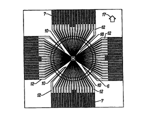
Also, as shown in Fig. 4, reference electrodes 10 are formed at four positions
on
lines extended from diagonals of the rectangular region in the central part of
the glass
substrate in which the microelectrodes are disposed. The reference electrodes
are
insulated from each other and from the microelectrodes. These reference
electrodes 10 are
also connected to the electric contacts 7 situated on four sides of the glass
substrate by the
conductive pattern 12 for wiring same as the microelectrodes 11. The reference
electrodes
10 are formed in the same process as the microelectrodes 11, as mentioned
below, but the
size is generally significantly larger than that of the microelectrodes 11
being, e.g., a
rectangle of about 200 microns in one side. Therefore, as compared with one of
the
microelectrodes 11 of about 50 microns square, the rectangular area is larger,
preferably
9
CA 02316213 2000-06-23
WO 99/34202 PCT/US98/27489
about 16 times larger, and, by this portion, the impedance of the reference
electrodes 10 is
smaller than the impedance of the microelectrodes 11.
The positions of the reference electrodes 10 are preferably on lines extending
from
the diagonals of the rectangular region in the central part of the glass
substrate in which the
microelectrodes 11 are disposed. The reference electrodes 10 in this variation
are located
about 6 mm from the center of the rectangular region. Said another way, they
are placed at
four comers of a square of about 8.5 mm in one side.
Moreover, as shown in Fig. 4, on each of the four sides of the glass substrate
may
be found 17 electric contacts 7. These electric contacts 7 are attached (one-
by-one) to each
of the 64 microelectrodes 11 and four reference electrodes 10 through the
conductive
pattern 12. The pitch of the 17 electric contacts is desirably spaced to the
pitch of 1.27
mm of the universal connector. The manufacturing process of this integrated
multiple
electrode 2 is explained below by referring to the sectional view in Fig. S.
The depiction
in Fig. 5, for the ease of explanation, is not to scale.
On the surface of a glass substrate 13, an ITO (indium tin oxide) film in a
thickness
of 150 nm is applied, and a conductive pattern 12 is formed by photo resist
and etching. A
negative photosensitive polyimide film of about 1.4 microns in thickness is
applied
thereon, and an insulating film 14 is formed. On portions of the
microelectrodes 11 (or
alternatively reference electrodes 10) and electric contacts 7, the ITO film
is exposed, and
nickel plating 15 of 500 nm in thickness and gold plating 16 of 50 nm in
thickness are then
applied.
A polystyrene or glass cylindrical member 6 corresponding to a wall of about
22 mm in inside diameter, about 25 mm in outside diameter, and 8 mm in height
may then
be placed on the central part of the glass substrate by using a Silicone
adhesive (see Fig. 2
and Fig. 4). A highly preferred adhesive is an RTV (Room Temperature
Vulcanization)
silicone rubber, particularly those which use an acid cure system. These
produce a low
level of toxicity because of the acetic acid produced during the cure step.
Two useful
varieties include KE42T (Shin-Etsu Silicone) and Silastic Medical Adhesive
Silicone Type
A (Dow Corning). A cylindrical wall member 6 is shown, but the wall may be
oval to
allow enhanced access to the sample. The wall member 6 is affixed in the
center of the
glass substrate, that is, in a state aligned with the central part of the
rectangular region in
which the 64 microelectrodes are disposed. In the region enclosed by this
cylindrical
CA 02316213 2000-06-23
WO 99/34202 PCT/US98/27489
member b, the cells or tissues are cultivated. This cylindrical member 6 is
filled, e.g., with
an aqueous solution of 1 wt.% of chloroplatinic acid, 0.01 wt.% of lead
acetate and 0.0025
wt.% of hydrochloric acid, and by passing a current of 20 mA/cm2 for a minute,
platinum
blacks 11 a (or alternatively, reference electrode platinum black 1 Oa) are
precipitated on the
surfaces of the microelectrodes 11 and reference electrodes 10.
The region within the cylindrical member 6 is occasionally referred to as the
"measuring region" which includes the area including both the microelectrodes
11 and
reference electrodes 10. It is further within the scope of the invention that
the reference
electrodes be placed on the inner surface of the cylindrical member 6.
At one corner of the integrated multiple electrode 2, an indexing or arrow
mark 17
showing the direction is provided. This arrow mark 17 can be formed in the
same
manufacturing process as the microelectrodes 11 and reference electrodes 10.
However,
the surface is coated with gold plating only, and platinum black is not
formed. The length
and width of the arrow mark 17 are both about 5 mm. Moreover, near one corner
of the
rectangular region of disposing the microelectrodes 11, a small indexing mark,
e.g., a
micro-mark 18 similar to the arrow mark is provided. This micro-mark 18 is not
visible by
the naked eye, but a same pattern as the arrow mark 17 is recognized in a
magnified view
by an optical observation device of the measuring apparatus, so that the
direction, position,
axes, etc. may be identified. Like the arrow mark 17, the micro-mark 18 can be
also
formed in the same manufacturing process as the microelectrodes 11 and
reference
electrodes 10.
In Fig. 2, the integrated multiple electrode 2 is sandwiched between holders
3, 4.
An electrical connection is made in the same way. The holders 3, 4 are
typically
polymeric. The step portion is used to hold the edge of the integrated
multiple electrode 2
and the rectangular opening are formed in the central part. The upper holder 3
is provided
with a pair of fasteners 8 and 17 pieces x 4 pairs of contact metal areas 9. A
top view of
the holders 3, 4 sandwiching and fixing the integrated multiple electrode 2 is
shown in Fig.
6(A), its side view (section B-B) in Fig. 6(B), and its perspective back view
in Fig. 7. As
clear from these diagrams, the fastener 8 is supported by and rotates about
shaft pins 8a on
two confronting sides of the upper holder 3. As shown in Figure 7, grooves 4a
are formed
in two confronting sides of the back side of the lower holder 4. Protrusions
8b of the
11
CA 02316213 2000-06-23
WO 99/34202 PCT/US98/27489
fastener 8 are fitted in grooves 4a and the upper and lower holders 3, 4 are
fixed firmly in a
state of sandwiching the integrated multiple electrode 2.
A total of 68 contact metal fittings 9 provided on the upper holder 3 to
correspond
to the electric contacts 7 of the integrated multiple electrode 2 may be
formed by
processing elastic and conductive metal plates such as a Be/Cu spring alloy,
plated with Ni
and Au. The metal fittings 9 have a sectional shape as shown in Fig. 8. That
is, it consists
of a pin 9a, its base part 9b, and a movable contact part 9d extending from
the base part 9b
through a curved part 9c. In such structure, the movable contact part 9d can
be elastically
dislocated from the base part 9b. In the upper holder 3, holes for inserting
the pin 9a of the
contact metal fitting 9, and grooves for fitting the base part 9b are formed
in 68 ( I 7 x 4)
positions.
As shown in Fig. 2 and Fig.6(B), with the contact metal fitting 9 inserted and
fixed
in the hole and groove, pin 9a projects from the upper holder 3. Contact metal
fittings 9
are of two types which differ in the length of the base part 9b. The two sized
fittings 9 are
alternately disposed, 16 pins 9a projecting from the upper holder 3 are
arranged in two
zigzag rows. As mentioned later, these pins 9a are connected to the connectors
mounted
on the printed wiring board 5 for connection with the outside.
Movable contact part 9d of the contact metal fitting 9 projects from the lower
side
of the upper holder 3, when in contact metal fitting 9 is inserted and affixed
in the hole and
groove of the upper bolder 3. With the holders 3, 4 fixed on both sides of the
integrated
multiple electrode 2, the movable contact part 9d of each contact metal
fitting 9 contacts
with the electric contact 7 of the integrated multiple electrode 2, and a
specified contact
pressure is given to the contact area by elastic deformation of the curved
part 9c. In this
way, the electric contacts 7 for connecting to the microelectrodes 11 and
reference
electrodes 10 of the integrated multiple electrode 2 through the conductive
pattern 12 are
electrically connected at a lower contact resistance (30 milliohms or less) as
compared
with that of the contact metal fittings 9.
As mentioned above, the holders 3, 4 firmly fixing the integrated multiple
electrode
2 in a state of electric contact with the integrated multiple electrode 2 are
electrically
connected and affixed to the printed wiring board 5 as shown in Fig. 2. The
electric
connection from the microelectrodes 11 and reference electrode 10 of the
integrated
multiple electrode 2 to the conductive pattern I2, electric contacts 7 and
contact metal
12
CA 02316213 2000-06-23
WO 99/34202 PCT/US98/27489
fittings 9 is further connected to the cell potential measuring apparatus
mentioned above
through the printed wiring board 5. Handling of the integrated multiple
electrode on the
measuring apparatus is facilitated by use of the printed wiring board 5.
Also as shown if Figure 2, printed circuit board 5 may be made up of, e.g., a
glass
epoxy two-sided substrate. Connectors Sa are provided at the back side of four
positions
on the circumference of the circular opening formed in the center of printed
circuit board
5. Since 16 pins 9a projecting in two zigzag rows from the four positions on
the surface of
the upper holder 3 are inserted into the individual corresponding connectors
Sa, the
assembly of the integrated multiple electrode 2 and holders 3, 4 is fixed to
the printed
wiring board 5 and is connected electrically.
At both edges Sb of the printed wiring board 5, electric contacts of 2.54 mm
pitch
for both edge connectors may be found. These electric contacts and central
connectors Sa
are connected in the conductive pattern Sc. The inside row of the both
connectors Sa is
wired by the surface pattern, and the outside row by the back side pattern,
respectively,
and 34 each on both surface and back sides of both edges Sb, that is, a total
of 68 electric
contacts are formed. To make the mechanical fixing secure, the upper holder 3
may be
affixed to the printed wiring board 5 by fastening with screws.
The reference electrodes 10 of the integrated multiple electrode 2 described
by
reference to Fig. 4. The reference electrodes 10 are usually immersed in the
culture fluid as
the reference potential for measuring the potential occurnng in each
microelectrode.
Therefore, each microelectrode i 1 is connected to an input of the amplifier
34 (Fig. I), and
the reference electrodes 10 are connected to the reference voltage terminals
of each
amplifier. The 64-channel amplifier is divided into four groups of 16 channels
each, and
each one of the four reference electrodes is commonly connected to the
reference voltage
terminal of one group for 16 channels.
First, as is clear from Fig. 4, it is preferred to position the four reference
electrodes
10 on extensions of diagonals of the central rectangular region containing the
microelectrodes 11. In general, this is a matter of convenience for pattern
wiring.
Moreover, in order to place the segments of cells or tissues easily so as to
cover all of 64
microelectrodes and not to cover the four reference electrodes, the distance
between the
central rectangular region disposing the microelectrodes 11 and the reference
electrodes 10
should be as large as reasonably possible. Moreover, by placing the four
reference
13
CA 02316213 2000-06-23
WO 99/34202 PCT/US98/27489
electrodes 10 at equal distances from the center of the rectangular region,
the noise level
occurring in each microelectrode is substantially uniform. Although the
positions of the
reference electrodes are closely specified above, the numerical values are not
intended to
be absolute, but are only intended to be guidelines.
The size of the reference electrodes 10 may be 4-64, preferably about 16,
times the
area of a microelectrode as mentioned above. As a result, the impedance is
balanced
between the measuring potential input side of the amplifier and the reference
potential
input side and the noise level is minimized. For instance, by forming the
microelectrodes
and reference electrodes in the same noted process and by setting the area of
the reference
electrode 16 times that of the microelectrode, the impedance of 16
microelectrodes and the
impedance of one reference electrode responsible are nearly equal.
Example
This Example shows the difference in noise level between a system including an
integrated multiple electrode such as that discussed above and reference
electrodes of SO
microns square and 200 microns square. Fig. 9 and Fig. 10 show those
comparative noise
levels.
We fabricated integrated multiple electrodes (such as shown in Fig. 4) having,
respectively, reference electrodes of SO microns square and reference
electrodes of 200
microns square. The integrated multiple electrodes each had cylindrical
members 6. The
same culture medium as normally used in tissue culturing was placed inside the
cylindrical
members 6. To limit the resulting signal to the noise, no cell or tissue
sample was placed
on the microelectrodes. As shown in Fig. 11, of the 64 microelectrodes, the
central seven
sites (channels I to S, 7, 8) were measured.
Fig. 9 shows the noise waveform of the reference electrodes in 50 microns
square,
and Fig. 10, 200 microns square. In each diagram, the voltage on the axis of
ordinates is
0.02 mV/div, and the time on the axis of abscissas is 5.0 ms/div. As clear
from
comparison between Fig. 9 and Fig. 10, the noise level is clearly smaller when
the
reference electrodes are 200 microns square (Fig. 10) as compared to reference
electrodes
with 50 microns square (Fig. 9). Incidentally, as described in relation to the
prior art, by
using one of the 64 microelectrodes as the reference electrode to be
responsible for 16
microelectrodes, the noise level was as large as in Fig. 9.
14
CA 02316213 2000-06-23
WO 99/34202 PCT/US98/27489
As described herein, according to the cell potential measuring electrode and
apparatus of the invention, the noise effect is small, and if positioning when
setting the
segments of cells or tissues to be measured is not very precise, all
microelectrodes are
effectively utilized, and potentials at multiple points can be measured
simultaneously.