Note: Descriptions are shown in the official language in which they were submitted.
CA 02316232 2007-12-24
1
A Method and Apparatus for Reducing Flicker in the Television Display of
Network
Application Data
Field of the Invention
The present invention relates to television systems, and more specifically to
a
method and apparatus for reducing flicker in the combined display of
television signals
and network application data on a television display screen.
Background of the Invention
Since the 1940's, television systems have been increasingly embraced by many
households, particularly in the industrial countries. Television systems have
generally
been used to view broadcasts made in distant parts of the world or to view a
pre-recorded
program from a video cassette player (VCP). A significant proportion of the
households
presently have at least one television set in their homes. Television displays
are presently
available or anticipated to be widely available in analog (e. g., NTSC analog
signal
displayed on a CRT based display screen) as well as digital technologies (e.
g., HDTV).
In parallel, data network applications (hereafter"network applications") have
experienced a phenomenal growth since the mid-1980s. Network applications such
as
web-browsing and electronic mail have had a fundamental impact on the manner
in
which information is exchanged and disseminated. These network applications
have
particularly been implemented for and used along with computer systems such as
personal computer systems, work-stations, and the like.
At least in view of the considerable presence of the television systems in the
households, it may be desirable to provide the capability to access the
network
applications on television systems. However, there may be several problems
which need
to be addressed to enable access of data network applications from television
systems.
For example, the system may need to be designed to appropriately process the
different forms/formats in which the signals of the network applications and
television
CA 02316232 2007-12-24
2
signal are received. As is well known, a television signal may be received in
an
interlaced format (e. g., composite television signal in NTSC format) and the
network
application data may be received in a non- interlaced format.
In addition, network application data may be characterized by sharp
transitions in
color (e. g., the display may include alternative scan lines of black and
white). In general,
the display of such transitions on television screens results in flicker. As
is well known in
the art, flicker on television displays is undesirable as it can cause
considerable strain on
human eyes.
Thus, what is needed is a method and apparatus which can display both the
interlaced television signal and the non-interlaced data network application
data on a
television display screen while reducing or eliminating flicker in the network
application
data display.
Summary of the Invention
The present invention is directed to a method and apparatus for displaying
network application data along with an image encoded in a television signal on
an
interlaced display screen of a television system. Flicker (that may otherwise
result) is
substantially reduced from the network application data display by filtering
the pixel data
elements as explained below.
A network interface receives network application data (e. g., from web
browsing)
from an external source. A display controller generates pixel data elements
representative
of an interlaced image of the network application data display and stores the
pixel data
elements in a memory module.
The display controller includes a flicker filter and an interlacer in one
embodiment of the present invention. The flicker filter receives the pixel
data elements
from the memory module and filters the received data to generate pixel data
elements
representing a smoothened image (i. e., an image without sharp transitions).
The set of
CA 02316232 2007-12-24
3
pixel data elements received and the set of pixel data elements generated by
the flicker
filter represent network application data display in an interlaced format. The
term
interlaced format refers to all consecutive lines of an image. In contrast,
non- interlaced
format includes only the alternate lines of an image.
The interlacer receives the pixel data elements of the smoothened image and
generates an interlaced image by providing pixel data elements representing
alternate
lines of the smoothened image. A selection circuit receives the pixel data
elements of the
interlaced image and an interlaced display signal included in a television
signal. The
selection circuit selects either the pixel data elements or the interlaced
display signal on a
point-by-point basis. That is, each point of the image encoded in the
television signal is
logically mapped to a point on the interlaced display screen. Similarly, each
pixel data
element is also mapped to a point on the interlaced display screen. Such
mappings allow
the selection circuit to select with the television signal image or the
network application
data image on a point-by-point basis.
In one embodiment of the present invention, the selection circuit includes a
digital
to analog converter (DAC) which converts each pixel data element generated by
the
interlacer into an analog display signal. An analog multiplexor is used to
select between
each of these analog display signals and the television signal on a point-by-
point basis.
An example implementation according to the present invention includes a timing
signal generator which controls and coordinates the operation of the memory
module,
interlacer, flicker filter. The timing signal generator generates a first
clock signal and a
second clock signal, with the first clock signal having a frequency of twice
the second
clock signal. The first clock signal is used to drive portions of the
embodiment, which
operate in non-interlaced mode, i. e., memory module, flicker filter, and
input portion of
the interlacer. The second clock signal is used to operate the portions of the
embodiment
which operate in interlaced mode, i. e., the output portion of the interlacer
and display
screen.
CA 02316232 2007-12-24
4
The present invention reduces flicker in the network application data display
as
the pixel data elements representative of the network application data display
are filtered.
By filtering the data elements, sharp transitions in display are reduced,
which results in
the elimination of flicker. The present invention achieves such flicker
reduction without
requiring substantial additional memory. This is accomplished by accessing
data from a
memory and performing the flicker reduction operation at twice the clock
frequency as
that used for providing the interlaced output. By providing data at twice the
clock
frequency, the present invention enables the flicker filter to have adjacent
lines of the
image for clicker reduction operation, while providing the output data from
the interlacer
at a rate required for display on a display screen.
The present invention is particularly suited for interlaced displays as the
network
application data display is transformed into an interlaced image, which can be
easily
combined with interlaced images typically present in television signals.
Further features and advantages of the invention, as well as the structure and
operation of various embodiments of the invention, are described in detail
below with
reference to the accompanying drawings. In the drawings, like reference
numbers
generally indicate identical, functionally similar, and/or structurally
similar elements.
The drawing in -which an element first appears is indicated by the leftmost
digit(s) in the -
corresponding reference number.
In accordance with a first aspect of the present invention, there is provided
a
television system for displaying an image corresponding to network application
data
along with an image encoded in a television signal, said television signal
including an
interlaced display signal and a plurality of synchronization signals, said
television system
comprising:
a sync extractor for extracting said plurality of synchronization signals from
said
television signal;
a color decoder for extracting said interlaced display signal from said
television
signal;
CA 02316232 2007-12-24
a network interface for receiving said network application data;
a memory module for storing a plurality of pixel data elements representative
of a
non-interlaced image of said network application data;
an interlaced display screen for displaying said image encoded in said
television
5 signal and said image corresponding to network application data;
a display controller coupled to said memory module, said display controller
receiving said plurality of pixel data elements representative of said non-
interlaced image
of said network application data, said display controller providing a
plurality of pixel data
elements representative of an interlaced image of said network application
data, said
display controller comprising:
a flicker filter for receiving said plurality of pixel data elements
representative of
said non-interlaced image, said flicker filter filtering said plurality of
pixel data elements
to generate a plurality of pixel data elements representative of a smoothened
non-
interlaced image; and
an interlacer for receiving said plurality of pixel data elements
representative of
said smoothened non-interlaced image, and generating another plurality of
pixel data
elements representative of said interlaced image, said interlaced image
including alternate
lines of said smoothened non-interlaced image;
a digital-to-analog converter (DAC) for converting each of said plurality of
pixel
data elements into an analog signal;
a multiplexor coupled to said DAC and said color decoder, said multiplexor
receiving each of said analog signals and said interlaced display signal, said
multiplexor
selecting as an output either each of said analog signals or said interlaced
display signal
on a point-by-point basis, wherein each of said analog signals received by
said
multiplexor and a corresponding portion of said interlaced display signal
correspond to a
same point on said interlaced display screen; and
a display interface for generating display signals to said interlaced display
screen
according to said output of said multiplexor to generate a combined image of
said image
encoded in said television signal and said image corresponding to said network
application data,
CA 02316232 2007-12-24
6
wherein flicker is substantially eliminated from said combined image because
of
the filtering operation of said flicker filter.
In accordance with a second aspect of the present invention, there is provided
a
display circuit implemented in a television system, said television system
including a
display screen capable of displaying interlaced images, said display circuit
enabling the
display of an image corresponding to network application data along with an
image
encoded in a television signal, said television signal including an interlaced
display signal
and a plurality of synchronization signals, said display circuit comprising:
a memory interface for receiving a plurality of pixel data elements
representative
of a non-interlaced image of said network application data, wherein said
plurality of pixel
data elements are stored in a memory module;
a flicker filter for receiving said plurality of pixel data elements
representative of
said non-interlaced image, said flicker filter filtering said plurality of
pixel data elements
to generate a plurality of pixel data elements representative of a smoothened
non-
interlaced image;
an interlacer for receiving said plurality of pixel data elements
representative of
said smoothened non-interlaced image, and generating another plurality of
pixel data
elements representative of an interlaced image, said interlaced image
including alternate
lines of said smoothened non-interlaced image;
wherein said interlaced image can be provided to a selection circuit,
said selection circuit also receiving said interlaced display signal and said
another
plurality of pixel data elements representative of said interlaced image of
said network
application data, said selection circuit generating a plurality of display
signals
representative of a combined image of said interlaced image of said network
application
data and said image encoded in said television display signal;
wherein said selection circuit generates said plurality of display signals
representative of said combined image by selecting either said interlaced
display signals
or each of said plurality of pixel data elements representative of said
interlaced image of
said network application data on a point-by-point basis, and
CA 02316232 2007-12-24
7
wherein said plurality of display signals can be used for generating said
combined
image on said interlaced display screen.
In accordance with a third aspect of the present invention, there is provided
a
display circuit implemented in a television system, said television system
including an
interlaced display screen, said display circuit enabling the display of an
image
corresponding to network application data along with an image encoded in a
television
signal, said television signal including an interlaced display signal and a
plurality of
synchronization signals, said display circuit comprising:
means for receiving a plurality of pixel data elements representative of a non-
interlaced image of said network application data;
means for filtering said plurality of pixel data elements to generate a
plurality of
pixel data elements representative of a smoothened non-interlaced image;
means for generating another plurality of pixel data elements representative
of an
interlaced image, said interlaced image including alternate lines of said
smoothened non-
interlaced image;
means for selecting either said interlaced display signals or each of said
another
plurality of pixel data elements representative of said interlaced image of
said network
application data on a point-by-point basis to generate a plurality of display
signals
representative of a combined image of said interlaced image of said network
application
data and said image encoded in said television display signal; and
means for generating said combined image on said interlaced display screen
according to said plurality of display signals representative of said combined
image.
In accordance with a fourth aspect of the present invention, there is provided
a
method of generating a combined display on an image represented by network
application data and an image encoded in a television display signal of a
television
system, said combined display being generated on an interlaced display screen,
said
television signal including an interlaced display signal and a plurality of
synchronization
signals, said method comprising the steps of:
CA 02316232 2007-12-24
8
receiving a plurality of pixel data elements representative of a non-
interlaced
image of said network application data;
filtering said plurality of pixel data elements to generate a plurality of
pixel data
elements representative of a smoothened non-interlaced image;
generating another plurality of pixel data elements representative of an
interlaced
image, said interlaced image including alternate lines of said smoothened non-
interlaced
image;
selecting either said interlaced display signals or each of said another
plurality of
pixel data elements representative of said interlaced image of said network
application
data on a point-by-point basis to generate a plurality of display signals
representative of
a combined image of said interlaced image of said network application data and
said
image encoded in said television display signal; and
generating said combined image on said interlaced display screen according to
said plurality of display signals representative of said combined image.
Brief Description of the Drawings
The present invention will be described with reference to the accompanying
drawings, wherein:
Figure 1 is a block diagram illustrating an example implementation of a
television
system in accordance with the present invention;
Figure 2 is a flow-chart illustrating the steps performed in accordance with
the
present invention;
Figure 3A is a block diagram illustrating an example display of network
application data on a television display screen;
Figure 3B is a block diagram of a memory module illustrating an example scheme
for storing pixel data elements representative of network application data for
display on a
television display screen of Figure 3A;
Figure 4 is a block diagram of an example implementation of a on-screen
display
(OSD) controller illustrating the manner in which filtered data is provided in
an
interlaced format;
CA 02316232 2007-12-24
9
Figure 5 is a block diagram of an example implementation of an interlacer
which
generates interlaced image data from non-interlaced image data;
Figures 6A and 6B illustrate the timing relationships between various signals
that
control the operation flow in one embodiment of the present invention; and
Figure 7 is a block diagram of a television system illustrating the problems
which
may be encountered without implementing one or more features of the present
invention.
Detailed Description of the Preferred Embodiments
1. Overview and Discussion of the Invention
The present invention is described in the context of a circuit implemented in
a
television system. In general, conventional television systems receive a
television signal
in an interlaced format and generate a display based on the received signal.
In accordance
with the present invention, network application data (such as a display
resulting from web
browsing and having non- interlaced format) is received from an external
source, and
displayed without much flicker on television display screens displaying
interlaced
images.
To reduce flicker which may otherwise result in the network application data
display, a circuit according to the present invention first receives pixel
data elements
representative of network application data in a non-interlaced format. As used
herein,
non-interlaced format of an image refers to all the lines of the image,
whereas interlaced
format refers to alternate lines of the image. The circuit filters the
received pixel data
elements using consecutive lines of the non- interlaced image to remove sharp
transitions,
and generates an interlaced image by providing alternate lines of the
interlaced filtered
image. The interlaced image of the network application data is then combined
with an
interlaced image encoded in a television signal. The final image generated by
such
combining can have portions of network application data display and television
signal
display as desired by a user.
As the data representing the image is filtered using adjacent lines of the non-
interlaced image, sharp transitions are removed from the final image. As a
result, flicker
CA 02316232 2007-12-24
is substantially eliminated. To appreciate the present invention, it is
helpful to understand
the problems that may be encountered with an example embodiment, which may not
incorporate one or more aspects of the present invention. Accordingly, one
such example
embodiment will be described first, followed by the present invention in
detail.
5
2. An Embodiment Which Does not Incorporate One or More Aspects of the
Invention
Figure 7 is a block diagram of a television system 700 illustrating some
problems
which may be encountered by not employing one or more aspects of the present
10 invention. Television system 700 includes sync extractor 705, color decoder
710, timing
generator 720, memory 730, memory controller 740, graphics data path 750, and
multiplexor 760. As will be described below, unlike the present invention, all
the
components of television system 700 operate in an interlaced mode while
combining the
display corresponding to the data stored in memory 730 with the image
represented by a
television signal.
Sync extractor 705 and color decoder 710 receive a television signal (e. g.,
composite video signal) on line 701. Sync extractor 705 extracts the
synchronization
signals (e. g., tv_hsync and tv_vsync) and provides the signals to timing
generator 720.
Color decoder 710 extracts a display signal portion representing an image
encoded in the
received television signal. The display signal portion is provided to
multiplexor 760
along 716. One of several products available in the market can be used for
sync extractor
705 and color decoder 710.
Timing generator 720 receives the television synchronization signals (tv_hsync
and tv vsync) and generates the timing signals (ICDE and 1VCLK) to graphics
data path
750. The timing signals operate to coordinate the operation of graphics data
path 750
with the received television signal. Specifically, graphics data path 750 uses
the timing
signals to match each point on the image encoded in the television signal with
each point
of the image represented by the data stored in memory 730. Memory 730 stores
the data,
the display of which is combined with the television signal display. Memory
controller
CA 02316232 2007-12-24
11
'. .
740 retrieves the data from memory 730 according to the memory access requests
received from graphics data path 750. The operation of graphics data path 750
is
explained below.
Graphics data path 750 receives the timing signals ICDE (interlaced composited
display enable) and 1 VCLK from timing generator 720. The 1 VCLK signal is
used by
graphics data path 750 to operate the intemal pipeline (s). The pipeline may
perform
functions such as determining whether to display the image encoded in the
received
television signal or the image represented by the data stored in memory 730 on
a point-
by-point basis. The blank signal 765 indicates whether to display the
television signal or
the data. The pipelines may perform other functions such as converting the
memory data
received at a memory-word width of memory 730 to a pixel element format
representative of points of an image.
Notably, graphics data path 750 operates entirely in interlaced format. That
is,
graphics data path 750 receives data from memory 730 in an interlaced format
(i. e.,
alternate lines of a network application data display frame). The data is
retrieved in an
interlaced format from memory 730 such that the retrieved data corresponds to
the point
of the television signal image when both are received at multiplexor 760.
Graphics data
path 750 generates as output a blank signal to indicate whether to display the
television
signal image or the data image. If data image is to be displayed, graphics
data path 750
generates as output pixel data elements which result from processing the
received data.
Digital to analog converter (DAC) 770 receives the pixel data elements from
graphics data path 750 and generates analog signals (e. g., in RGB format)
therefrom.
The analog signals generated from the data stored in memory 730 is provided to
multiplexor 760. Multiplexor 760 selects either analog signal received from
DAC 770 or
the television display signal received from color decoder 710 according to the
value on
the blank signal 765. The selection results in combining the television signal
display with
the data display. The output of multiplexor 760 is used to generate display
signals on a
television screen.
CA 02316232 2007-12-24
12
One problem with the above system is that considerable flicker may be present
in
the data display portion should there be sharp transitions in the display. To
avoid such
undesirable flicker, the data design (e. g., font bit maps or palettes) in
memory 730 may
be chosen such that sharp transitions are not present. Unfortunately, such a
system may
not be adequate when the data is received from external sources such as web
browsing
because the data can be with several sharp transitions. In addition, as the
data is retrieved
in an interlaced format, data for adjacent lines may not be present for
achieving effective
filtering which may reduce filter.
As will be explained below, the present invention overcomes these problems by
first retrieving the data in a non-interlaced format so that adjacent lines
are available for
performing effective filtering. After filtering the data, the resulting
filtered data is
provided in an interlaced format suitable for display on a television screen.
3. The present invention
The present invention is explained with reference to the flow-chart of Figure
2,
which illustrates the steps performed in displaying network application data
and
television signal on a television screen between the begin step 201 and the
end step 299.
In step 210, network application data is stored in a memory. The data can be
stored in any
format, including but not limited to, -text, bit-maps, HTML, VRML etc.
In step 220, pixel data elements representing network application data in a
non-
interlaced format are retrieved. The conversion of network application data
into pixel
data elements can be performed either before storing in the memory or after
retrieving
network application data from the memory. The pixel data elements together
represent an
image corresponding to the display of network application data.
In step 230, the pixel data elements representing network application data are
filtered. Filtering has the general effect of smoothing out the image (by
eliminating or
reducing sharp transitions) corresponding to network application data. As a
result of
smoothing, flicker may be reduced from network application data display. It
may be
CA 02316232 2007-12-24
13
'. .
noted that at the time of filtering, the network application data is
represented in non-
interlaced format. That is, filtering is based on a complete image
representing network
application data.
In step 240, the pixel data elements of the alternate image lines of the
filtered
image are provided for subsequent processing. Each set of alternate lines
represents an
interlaced frame. Odd and even lines may be provided alternatively. Thus, the
filtered
image is provided in an interlaced format for subsequent processing.
In step 250, each pixel data element of the interlaced image is converted to a
corresponding analog signal. In step 260, the television display signal and
the analog
signals representing the pixel data elements in interlaced format are
received. One of the
two signals is selected for display on an interlaced television display
screen. The
selection can be done on a pixel-by-pixel basis. That is, the image of each
display entity
can be logically mapped to a point on the television display screen, and a
pixel data
element of one of the two display entities can be selected.
Thus, by providing the non-interlaced image of network application data as
interlaced frames, the present invention enables the display to be selected on
a point-by-
point basis. In addition, as the network application data image is filtered,
flicker may be
avoided in network application display. Also, as the network application data
is retrieved
in a non-interlaced mode (progressive scan mode), large memories can be
avoided for the
filtering processing while using several adjacent lines.
The present invention will now be explained in fiu-ther detail with reference
to
one or more example embodiments.
4. Example Environment
In a broad sense, the present invention can be implemented in any television
system. For
purposes of illustration, the invention will be explained in the context of a
television
system implemented using analog (e. g., using CRTs) technology. However, it
will be
CA 02316232 2007-12-24
14
apparent to one skilled in the art how to implement the present invention with
digital
technologies (e. g., HDTV supporting interlaced format) without departing from
the
scope and spirit of the present invention by reading the description herein.
Figure 1 is a block diagram of an example television system (TV) 100 in which
the present invention can be implemented. The operation, structure and use of
television
system 100 as relevant to the present invention will be explained here.
However, an
embodiment of television system 100 is explained in further detail in US
Patent
5,946,051.
Television system 100 comprises sync extractor 120, color decoder 130,
multiplexor 140, display interface 145, display screen 150, peripheral
interface 160, on-
screen-display (OSD) controller 170, digital-to-analog converter (DAC) 175,
memory
controller 185, memory module 180, and micro-controller 190. Micro-controller
190
generates control and clocking signals to coordinate and control the operation
of the
remaining components of television system 100. For purpose of clarity, only
some of the
connections from micro-controller 190 are shown in Figure 1. Each of the
components of
TV 100 are explained in further detail below.
Network interface 110 receives network application data from an external
source.
Network interface 110 can be a telephone modem, cable modem or any other
interface
which is designed to operate with the external source. The external source can
be, for
example, a dial-up connection (point-to-point) or a network connection
implemented
using a communication protocol. Even though network interface 110 is shown as
a single
block, it should be understood that it may contain more than one unit
depending on the
specific requirements of the individual television system.
Network interface 110 receives data corresponding to a network application
such
as web- browsing, electronic mail in a known way. The data may be received in
one of
known formats such as ASCII, HTML, VRML etc., which are encoded as electrical
CA 02316232 2007-12-24
signals. Network interface 110 sends signals representative of the network
application
data to OSD Controller 170.
OSD Controller 170 receives network application data from network interface
5 110, and stores the received data in memory module 180 by interfacing at 186
with
memory controller 185. Memory module 180 may include one or more physical
memory
units as suitable for the specific requirements for which TV 100 is designed
for. Memory
controller 185 interfaces with OSD controller 170, and enables OSD controller
170 to
store and retrieve data from memory module 180. The implementation of memory
10 controller 185 depends on the specific technology chosen for memory module
180, and
can be provided integral to a memory storage unit. Some features of an
embodiment of
memory controller 185 are described in US Patent 5,990,969.
OSD Controller 170 transforms the network application data as is suitable for
15 storage and retrieval from memory module 180. The storage scheme may
include
conventions to represent the area on which network application data is to be
displayed. In
one example embodiment, OSD controller 170 stores the network application data
as a
"bit map" encoded in RGB format in memory module 180 as illustrated with
reference to
Figures 3A and 3B, which are explained in further detail below.
OSD controller 170 may be designed to store other display entities as well.
These
display entities may provide additional capabilities or enhance the ease of
use of
television system 100. However these other display entities will not be
described here as
they may not be relevant to an understanding of the present invention. For the
purpose of
explaining the present invention, it will be assumed that OSD controller 170
stores only
network application data in memory module 180. For details of other display
entities
which may be stored in memory module and the manner in which they are used,
the
reader is referred to US Patent 5,946,051.
Also, OSD controller 180 receives pixel elements of network application data
image in a non-interlaced format from memory controller 185, but provides
pixel
CA 02316232 2007-12-24
16
elements corresponding to an image of an interlaced format. This conversion
simplifies
the overlay process between the television signal display and network
application data
display. In addition, OSD controller 180 filters the pixel data elements
received to
smooth out the network application data image. The pixel data elements
representing the
smoothened image (i. e., without sharp transitions) is provided in the
interlaced format.
The manner in which the filtering and interlacing is performed in an
embodiment is
described in detail below and in US Patent 6,072,530.
Digital-to-analog converter (DAC) 175 receives the pixel data elements
representing the smoothened image from OSD controller 170 and generates analog
display signals on line 174 from the pixel data elements. Each pixel data
element
typically represents the color of a point on display screen 150 when line 141
indicates
that network application data is to be displayed.
Sync extractor 120 and color decoder 130 receive a television signal 101 from
sources such as cable service providers, television (relay) stations, digital
video disk
players etc. The TV signal is generally received in a known format, for
example, in
NTSC composite video format. However, the television signal can be any other
signal
including an interlaced display signal and corresponding synchronization
signals.
Decoder 130 extracts the interlaced display signal which is encoded in the
television
signal and provides the display signal to multiplexer 140 on display signal
line 134.
Sync extractor 120 extracts (or generates) synchronization signals present in
the
television signal in a known way. The synchronization signals are provided to
micro-
controller 190 and OSD controller 170 to coordinate the network application
data flow
consistent with the reception of the television signal. In one embodiment
(described in
US Patent 6,177,959), the clock signal driving the OSD controller 170 are
genlocked to
the synchronization signals.
Multiplexor 140 receives the interlaced television signal and the analog
display
signals as inputs on lines 134 and 174 respectively, and selectively forwards
one of the
CA 02316232 2007-12-24
17
', .
two inputs to display panel interface 145 under the control of select line
141. The select
line is controlled by OSD controller 170 in one embodiment. As the two signals
received
on lines 134 and 174 correspond to the same point on display screen, the
selection is
performed on a point-by-point basis. The selection results in an overlay.
Thus, the
television signal display and network application data display are overlayed
before a
unified display is provided on display screen 150. From the description
herein, it will be
apparent that multiplexor 140 along with OSD controller 170 form a selection
circuit to
overlay the display entities displayed by television 100. In one embodiment,
select line
141 is controlled by OSD Controller 170 and each multiplexor input corresponds
to a
single pixel on display screen 150.
Multiplexor 140 along with select line 141 operates to select between the
television signal and the pixel data received on line 141. Even though the
processing of
television signal and network application data is explained with reference to
RGB data, it
should be understood that the present invention can be implemented using other
data
formats also without departing from the scope and spirit of the present
invention.
In the description above, multiplexor 140 and DAC 175 operate as a selection
circuit. The selection circuit operates in an analog domain in the sense that
the inputs to
multiplexor 140 are in the form of analog signals. However, it should be
understood that
the selection can be performed in a digital domain as well without departing
from the
scope and spirit from the present invention. Such a digital operation is
described in US
Patent 5,946,051.
Display interface 145 receives display signals from multiplexor 140, and
provides
any signaling interface required for display on display screen 150. If display
screen 150 is
implemented as a CRT screen, display interface 145 generates electrical
signals to control
the scan circuitry usually associated with CRT screens. The design and
implementation
of display interface 145 depends on the specific technology chosen for display
screen
150. The implementation of display interface 145 will be apparent to one
skilled in the
art. It is contemplated that the present invention can be implemented with
technologies
CA 02316232 2007-12-24
18
such as digital television systems (e. g., HDTV) and flat-panel based TVs,
projection TVs
based on DMD (digital mirror display) and the like.
Micro-controller 190 receives these synchronization signals on line 129 and
configures the remaining components based on the synchronization signals. For
example,
micro-controller 190 causes the creation of bit-maps corresponding to the
received
network application data. In addition, micro-controller 190 ensures that the
pixel data
elements received on lines 134 (for television signal) and 178 (the overlayed
image of
display entities stored in memory module 180) correspond to the same
point/pixel on
display screen 150.
Peripheral interface 160 can include an interface for one or more peripherals.
In
one embodiment, interfaces are provided for push-buttons and infra-red remote.
Push-
buttons can be found on conventional television sets, and are generally used
for functions
such as turning the television set ON/OFF, volume control etc. Infra-red
remote interface
operates in conjunction with remote control devices, which may be used for
several
functions such as television control (tuning, voice control, remote control
etc.), enabling
network applications etc. Devices such as key-boards which facilitate easy
entry of
ASCII data can be interfaced using infra-red interfaces. The implementation of
these
interfaces will be apparent to one skilled in the relevant arts based on the
disclosure
provided herein.
Thus, in one embodiment, OSD controller 170 of the present invention retrieves
the network application data from memory module 180 in a non-interlaced
format, filters
the received data to smoothen the image represented by the application data,
and provides
data representative of the smoothened image in an interlaced format. The data
is
converted into analog display signals. Multiplexor 140 selects either the
analog display
signals of network application data or television display signal for each
point on the
display screen. The selected signal is displayed on the corresponding point.
CA 02316232 2007-12-24
19
5. Storage in Memory Module in an Example Implementation
In an example implementation, network application data is stored in memory
module 180 according to the display sought on display screen 150. Typically, a
user
specifies the portion on display screen 150 on which network application data
is to be
displayed and the portion on which television signal is to be displayed. Micro-
controller
190 generates commands to store network application data in memory module to
correspond to the user specification. Data is stored in memory module
according to these
commands. OSD controller 170 is designed to receive this data and generate a
display in
the area specified by the user. Figure 3A illustrates the data format stored
corresponding
to a desired display illustrated in Figure 3B. The structure and operation of
OSD
controller 170 which uses the data format will then be explained with
reference to Figure
4.
In Figure 3B, network application data display 360 is shown on a portion of
display screen 150. Network application data display 360 can occupy all the
surface of
display screen 150 if so specified by a user. If network application data
display 360 does
not occupy the whole surface of display screen 150, television signal display
350 can
occupy the area outside of the network application data display 360. The
displays shown
in Figure 3B are examples only. The television signal display and network data
application can be combined in various ways, for example, as specified by a
user. Some
of the ways in which the display can be combined is explained in further
detail in US
Patent 5,946,051.
Figure 3B includes points A, B, C, D which illustrates in combination with
Figure
3A one convention according to which network application data is represented
in
memory module 180. The stored data defines the manner in which network
application
data display is to be combined with television signal display. In Figure 3A,
memory
module 180 is shown storing a bit map, with each bit position corresponding to
a point on
the display screen 150. The bit map can be stored as a surface, with each bit
having a
coordinate position. Each frame of the television signal also can be viewed as
a surface
CA 02316232 2007-12-24
with the same coordinate positions for like relative positions in the surface.
Thus, upper
left corner of display screen 150 is shown with X, Y coordinates of (0,0).
Each bit/point/pixel stored in display memory can generally have a value to
5 represent the display signals to be generated. In one embodiment, each point
of the
display is represented in pelletized 8 bits per pixel format. That is, the
eight bits are latter
mapped to a color (preferably in OSD controller 170 of Figure 1).
Continuing with the description of Figures 3A and 3B, point values A, B, C,
and
10 D stored in memory 180 correspond to points A, B, C, D of Figure 3B. Each
value (pixel
data element) stored in memory 180 is set to a value representing the color
with which a
corresponding point is to be displayed. However, if a television signal is to
be displayed
at the corresponding point, the value is set to a special value, termed
transparent color.
Thus, values corresponding to points C and D (on which the television signal
is
15 displayed) of Figure 3B are set to the transparent color. These values can
be set
according to the area in which a user desires to have the network application
data
displayed.
The manner in which an implementation of OSD controller 170 uses the above
20 convention to combine the network application data display with the
television signal
display is explained in detail below and in US Patent 5,946,051. The manner in
which
OSD controller 170 generates filtered interlaced displays in an embodiment of
the present
invention will be described below.
6. Example Implementation of OSD Controller
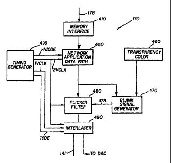
Figure 4 is a block diagram illustrating an example implementation of OSD
controller 170 comprising memory interface 410, transparency color register
460,
network application data path 450, blank signal generator 470, flicker filter
480,
interlacer 490, and timing generator 499. If other display entities are stored
in memory
module 180, OSD controller 170 can include other components to process these
other
CA 02316232 2007-12-24
21
display entities. An example implementation processing such display entities
is described
in US Patent 5,946,051.
Memory interface 410 is designed to have the electrical and other protocol
functions to interact with memory controller 185 and to provide the pixel data
elements to
data path 450. The output of memory interface 410 is coupled to the input of
network
application data path 450. Blank generator 470 and flicker filter 480 are
coupled to the
output of network application data path 450. Blank generator 470 is coupled to
transparent color register 460. Interlacer 490 is coupled to the output of
flicker filter 480.
Timing generator 499 is coupled to all the other components of OSD controller
170, but
only some of the connections are shown for clarity.
The operation of the components of OSD controller 170 can be appreciated by a
broad understanding of the speeds at which the components operate. Broadly,
network
application data path 450 and flicker filter 480 are clocked to operate at
high speed so as
to generate all the pixel data elements representing a non-interlaced image.
Interlacer 490
receives the pixel data elements at the high speed, but provides as output
smaller set of
pixel data elements representing an interlaced image. That is, during one
frame of the
television signal, pixel data elements representing all the odd lines are
provided, and
during an immediate frame, pixel data elements representing all the even lines
are
provided. Accordingly, the higher speed clock signal 2VCLK is shown connected
to
network application data path 450, flicker filter 480, and interlacer 490. The
slower
speed clock 1VCLK is shown connected to interlacer 490 only.
The individual components of OSD controller 170 are explained now in detail.
Data is received by network application data path 450, typically in response
to
commands from micro-controller 190 to memory controller 185. The commands
include
operations to store and retrieve data from memory module 180. Micro-controller
190 can
execute programs defined by data retrieved as a result of execution of the
commands.
Some of the retrieved commands cause data to be transferred to data path 450,
and the
CA 02316232 2007-12-24
22
transferred data may correspond to the pallette data stored in the respective
data paths.
The pallette data may be stored in another ROM (not shown).
The store commands cause data to be stored in memory module 180. Such data is
typically stored to modify (or define) a corresponding surface. For example,
if television
100 receives additional network data from an external source, the received
data may be
stored in memory module 180, preferably as a bit map. Continuing with the
description of
memory interface 410 with reference to Figure 4, memory interface 410
retrieves pixel
data elements upon receiving commands from network application data path 450.
Each
retrieved pixel data element corresponds to a specific pixel position on
display screen
150. Network application data path 450 receives multiple pixel data elements
in each
word from memory interface 410. Network application data path 450 then
performs steps
such as serialization to extract each pixel data element from the received
word. For
example, if network application data is encoded in 8 bpp format and if each
received
word includes 16 bits of pixel data, network application data path 450
serializes the 16
bits into two pixel data elements.
Network application data path 450 may further include a palette table to
convert
the 8 bits of pixel data into color data with more number of bits in a known
way. For
example, each pixel data element may be mapped into 5: 6: 5 or 6: 6: 6 RGB
data. The
pallette table in turn may be loaded (from an external ROM, not shown) by
appropriate
data in response to commands from micro-controller 190.
Network application data path 450 is shown operating using two clock signals
2VLCK and NICDE (non-interlaced composite display enable). The 2VCLK signal
indicates that it operates at twice the frequency as the 1 VCLK shown
connected to
interlacer 490. With the higher speed (frequency), the 2VLCK causes network
application data path 450 to operate with pixel data elements representing
images in a
non-interlaced format. The NICDE signal indicates the correct time for network
application data path 450 to start the pipelines and continue processing the
pixel data
elements. The pixel data elements are provided to interlacer 490 as a result
of such
CA 02316232 2007-12-24
23
processing. The pipelines in network application data path 450 are operated
such that
there is adequate data flow to interlacer 490.
Blank signal generator 470 generates a blank signal. In one embodiment, blank
signal generator 470 comprises a comparator, which compares the output of
network
application data path 450 with a transparency color stored in the programmable
register
460. The output of the comparator is provided to multiplexor 140 on line 141.
Thus, if the
two input values to the comparator are detected to be equal, the blank signal
is asserted,
which causes multiplexor 140 to select the data provided by OSD controller 170
on line
174. Otherwise, multiplexor 140 selects the television signal data received
from decoder
130.
In one embodiment, blank generator 470 provides the blank signal to flicker
filter
480 on bus 478. In turn, flicker filter 480 stores and/or transfers data bits
representative
of these signals correlated with the pixel data received from data path 450.
Such a
correlation allows OSD controller 170 to appropriately process corresponding
portion
(point) of television signal received in another path. In alternative
embodiments, the
blank signals can be provided directly to the selection circuit.
Flicker filter 480 can filter the received pixel data element in one of
several ways.
The received pixel data elements shall be referred to as'original pixel data
elements'and
the pixel data elements resulting from the filtering operation shall be
referred to as
'filtered pixel data elements'.
An example embodiment of flicker filter 480 is described in detail in US
Patent
6,072,530. Filtering generally has the effect of smoothing the image
eventually
displayed. As a result of image smoothing, flicker may be reduced in the
display of
network application data on display screen 150. In one embodiment, flicker
filter 480
includes a buffer to store two or more lines of data. However, a different
number of lines
can be stored and used during filtering as will be apparent to one skilled in
the relevant
arts by reading the description provided herein.
CA 02316232 2007-12-24
24
Filtering may be performed relative to both previous lines andlor subsequent
lines. In general, the data (corresponding to the adjacent lines) stored in
the buffer are
processed to remove (reduce) sharp transitions. For example, the pixel data
elements may
be interpolated with adjacent pixel data elements to generate the filtered
pixel data
elements. These filtered pixel data elements are used for generating display
signals as
explained below. Also, flicker filter 480 also operates using 2VLCK signal to
be able to
process the larger number of pixel data elements present in the non-interlaced
image. It
should be noted that a new pixel data value is typically generated by the
operation of
flicker filter 480. Accordingly, the blank signal is generated before pixel
data elements
are processed by flicker filter 480. Interlacer 490 receives pixel data
elements
representing a non-interlaced image from flicker filter 480, and provides as
output
alternate lines representing an interlaced image. Odd lines and even lines can
generally be
provided alternately. Each set of such alternate lines may be referred to as
an interlaced
frame. The conversion is performed as display screen 150 is designed to
display an
interlaced image. An embodirnent of interlacer 490 which is integrated into
the
architecture of flicker filter 480 is described in further detail in US Patent
6,072,530.
The operation of interlacer 490 can be controlled by the timing signals
generator
499. Specifically, ICDE (interlaced composite display enable), 2VCLK and I
VCLK
signals are shown in Figure 4 from time signals generator 499 to interlacer
490. 2VCLK
signal is generated at twice the frequency of 1VCLK signal. 2VLCK signal
enables
interlacer 490 to receive the pixel data elements representative of the image
in an non-
interlaced format. 1 VLCK signal enables interlacer 490 to generate pixel data
elements
representative of the same image in the interlaced format. ICDE is timed to
cause
interlacer 490 to generate each pixel data element which corresponds to a
point
represented by the television display signal portion received at multiplexor
140. As noted
earlier, multiplexor 140 can select one of the two signals, which results in
combining of
the television signal image and network application data image. Several
implementations
of interlacer 490 will be apparent to one skilled in the art by reading the
description
provided herein.
CA 02316232 2007-12-24
The output of interlacer 490 is provided as an input to multiplexor 140 on
line
174. As will be apparent from the description above, the output of interlacer
490
represents the network application data image in an interlaced format. In
addition, the
5 blank signal generated by data path multiplexor 460 is provided on signal
line 141. One
value of blank signal causes multiplexor 140 to select the television signal
pixel data
element received from decoder 130, and the other value of the blank signal
line causes
multiplexor 140 to select the pixel data element received from interlacer 490.
Thus, the
blank signal determines whether the television signal image or the network
application
10 data image is displayed on a pixel-by-pixel basis.
Timing signals generator 499 generates the clocking and control signals for
different components of OSD controller 170. Timing signals generator 499
receives as
input the HSYNC and VSYNC signals from the television signal, and generates
the
15 1 VLCK signals and display enable signals described herein. The 1 VLCK
signals and
display enable signals are'genlocked' to the television signal synchronization
signal.
Genlocking refers to the synchronization of one signal (s) to the other. It is
generally
important that the 1 VLCK and display enable signals be locked accurately to
the HSYNC
and VSYNC signals. Without such locking, the network data display may be seen
to be
20 moving with respect to the television signal display. Such movement (called
jitter) is
stressful on the human eye, and thus undesirable. When the signals are
genlocked
properly, jitters can be minimized (or eliminated). An embodiment for
achieving such
genlock is described in US Patent 6,177,959.
25 Thus, timing signals generator 499 generates timing signals which are
genlocked
with synchronization signals present in the received television signals. These
signals are
used to generate network application data in a non-interlaced mode. This
retrieved data is
filtered to smoothen (eliminate sharp transitions) in the network application
data image.
The data corresponding to the smoothened image is then provided in an
interlaced format
suitable for display on a interlaced television signal display. An example
embodiment of
interlacer 490 and the associated timing diagrams are described below in
detail.
CA 02316232 2007-12-24
26
7. Example Embodiment of Interlacer
Figure 5 is a block diagram of interlacer 490 in an example implementation of
the
present invention. Interlacer 490 comprises demultiplexor 510, arbiter 520,
write buffer
530, write buffer control 540, line buffer 550, read buffer 560, read buffer
controller 570,
demultiplexor 580, and tristate buffer 590. As will be explained, interlacer
490 receives
filtered pixel data elements (from flicker filter 480) representing non-
interlaced images
and generates pixel data elements representing non-interlaced images.
In one embodiment, line buffer 550 is implemented as a random access memory
having sufficient storage to store two horizontal lines of pixel data
elements. The word
width (i. e., number of bits in each word) of line buffer 550 can be chosen to
store data
for two pixel data elements. As will be clear from the discussion below, such
a memory
size and word width enables data to be delivered from interlacer 490 at a
desired rate
while effectively resolving conflicts for reading and writing into line buffer
550. The
remaining logic in interlacer 490 is implemented to operate with line buffer
550.
As the data output rate of interlacer 490 is only half that of the input rate
when
providing interlaced output, read operations can occur at half the frequency
as that of
write operations. Accordingly, write buffer control 540 and read buffer
control 570 are
coupled to 2VCLK and 1 VCLK signals respectively. In one embodiment, 2VCLK and
1VCLK operate at frequencies of 25 MHZ and 12.51VIHZ respectively.
In addition, NICDE (non-interlaced composite display enable) provides an
indication as to the clock cycles during which valid pixel data elements
representing the
non-interlaced image should be received. Accordingly, write buffer control 540
generates
signals on line 543 to enable write-buffer 530 to receive data from
demultiplexor 510 as
explained below in further detail. Write buffer control 540 sends a write
request to
arbiter 520 on line 524, which ensures there are no conflicts with read
operations to line
buffer 550.
CA 02316232 2007-12-24
27
As to the write operation into line buffer 550, write buffer 530 comprises two
portions 531 and 532, with each portion designed to store a pixel data
element. Once
stored, the two pixel data elements are forwarded to line buffer 550. In
another
embodiment, data is stored into and retrieved from line buffer 550 in units of
five pixel
data elements. Accordingly, write buffer 530 (and read buffer 560) may
comprise five
portions (instead of the two shown).
Demultiplexor 510 operates to multiplex pixel data elements received from
flicker
filter 480 into the two portions 531 and 532 under the control of multiplexor
selector line
541 asserted by write buffer control 540. Write buffer control 540 generates
the control
signals to write-buffer 530 and demultiplexor 510 to coordinate and control
the respective
operations. Write buffer control 540 also drives tri-state buffer 590 to a
high-impedance
state when data is read from line buffer 550.
As to the read operations, read buffer 560 can include two portions 561 and
562,
each for storing a pixel data element. When the first two pixel data elements
of a line are
available in write buffer 530, the two pixel data elements are directly
transferred to read
buffer 560. This is done to pre-fill read buffer 560 and keep the first two
data pixels ready
for display. Subsequent pixels to read buffer 560 are transferred from line
buffer 550.
Read buffer control 570 generates the control signals to coordinate and
control the read
operations.
The signals generated by read buffer control 570 further operate to serialize
the
pixel data elements stored in portions 561 and 562. That is, read buffer
control 570
generates appropriate values on signal line 578 to cause one of the two pixel
data
elements stored in read buffer 560 to be provided as output on line 174.
Signal line 578 is
asserted such that the earlier pixel data element in the scan order is
selected first.
Arbiter 520 arbitrates between read and write requests. Such arbitration may
be
required to avoid race conditions and as line buffer 550 may be implemented as
a single-
ported RAM. In general, if there is a conflict, arbiter 520 can provide higher
priority to
CA 02316232 2007-12-24
28
write requests as read transactions are received at lower frequency during
interlaced
mode of provision of data. Thus, in situations of conflict, read operations
may be serviced
during an immediately following clock cycle. By having two portions in read
buffer 570,
starvation may be avoided. That is, data will be provided continuously at a
desired rate
for generating display.
The operation of the individual components are controlled and coordinated
(synchronized) by signals from timing signals generator 499. The relationship
between
the timing signals in an example embodiment are illustrated with reference to
timing
diagrams below.
8. Timing Diagrams
Figures 6A and 6B illustrate the timing relationship between various signals
that
control the operation flow in one embodiment of the present invention.
Specifically,
Figures 6A and 6B respectively illustrate the horizontal and vertical timing
relationships.
The signals in each Figure are explained in detail below.
With reference to Figure 6A, HSYNC signal refers to the horizontal
synchronization signal extracted from the received composite television
signal. SYNC-
PULSE is generated in a known- way and is used to genlock the signals
including
1 VLCK and 2VCLK signals to the trailing edge of HSYNC. IHDE (interlaced
horizontal
display enable) signal controls the timing of the display of each horizontal
line on
television display screen 150. NIHDE (non-interlaced horizontal display
enable) signal
controls the timing of the flow of individual pixel data elements in a
horizontal line.
Horizontal display enable signals typically indicate the time during which
valid data is
present for subsequent processing. The NIHDE signal has to be ahead of the
IHDE by
sufficient VCLK clock cycles such that enough data is already in the
interlacer buffer
when IHDE starts. VCLK genlocked to HSYNC is used to generate both the
waveforms.
With reference to Figure 6B, NICDE signal controls the flow of data in network
application data path 340, flicker filter 480, and interlacer 490 as explained
above. The
CA 02316232 2007-12-24
29
horizontal lines (numbered 1-6) of each frame are processed during each period
when the
signal is at a logical high. The horizontal lines are referred by numbers 1-6
for
illustration. The ICDE signal is represented by odd ICDE and even ICDE signals
respectively when odd and even frames are processed. As can be appreciated,
the pixel
data elements generated from interlacer 490 have different values compared to
pixel data
elements provided as input to flicker filter 480 due to the filtering
operation.
Accordingly, the lines corresponding to NICDE are shown without prime symbol
('),
while the corresponding filtered data is shown with a prime symbol. Also, the
ICDE
signals are generated to ensure that the display signals generated from the
pixel data
elements are received at a time corresponding to corresponding portions of the
television
display signal portion at multiplexor 140.
Thus, using these signals, the combined display of network application data
and
television signal is generated. As all the horizontal lines of the network
application data
image are used for filtering, sharp transitions are reduced. As a result,
flicker may be
substantially reduced in the fmal network application data display on
television display
screen 150. In addition, as the filtered data is provided in an interlaced
format, it is well-
suited for display on interlaced displays of display screen 150.
9. Conclusion
While various embodiments of the present invention have been described above,
it should be understood that they have been presented by way of example only,
and not
limitation. Thus, the breadth and scope of the present invention should not be
limited by
any of the above-described embodiments, but should be defined only in
accordance with
the following claims and their equivalents.