Note: Descriptions are shown in the official language in which they were submitted.
CA 02316302 2000-06-23
WO 00/25343 PCT/US99/22221
RASTER SCAN GAUSSIAN BEAM WRITING STRATEGY AND METHOD FOR
PATTERN GENERATION
BACKGROUND OF THE INVENTION
Field of Invention
This invention relates generally to a lithographic system for pattern
generation. More
specifically it relates to a lithographic system having a raster scanned,
Gaussian beam writing
strategy for exposing a pattern.
1 o Description of the Related Art
Lithographic systems typically generate or expose patterns by controlling the
flow of
energy from a source to a substrate coated with a layer sensitive to that form
of energy.
Pattern exposure is controlled and broken into discrete units commonly
referred to as flashes,
wherein a flash is that portion of the pattern exposed during one cycle of an
exposure
1 s sequence. Flashes are produced by allowing energy from the source, for
example light,
electron or other particle beams, to reach the coated substrate within
selected pattern areas.
The details of flash composition, dose and exposure sequence used to produce a
pattern, and
hence the control of the lithographic system, make up what is known as a
writing strategy.
Writing strategies strive for both the highest pattern throughput and best
pattern
2 o quality. However, often highest throughput is only possible at the cost of
degraded pattern
quality. For example, smaller flashes usually result in better pattern quality
but lower
throughput. Thus an optimized writing strategy is one that makes the best
compromise for
each specific task. Both vector scan and raster scan writing strategies strive
for the same
goals, therefore a combination of elements of each may result in a better
compromise.
2s A traditional raster scan writing strategy employs a uniform periodic
raster scan, much
like a television. A mechanical stage moves a substrate uniformly in a
direction orthogonal to
CA 02316302 2000-06-23
WO 00/25343 PCT/US99/22221
-2-
the direction of the uniform scan of an energy beam. In this manner a pattern
is composed on
a regular grid with a regular scan trajectory resulting from the orthogonal
movement of the
stage and beam. When the beam is positioned over a grid site requiring
exposure, the beam is
unblanked and the underlying site exposed. Only the amount of dose, or energy,
at each site
s is varied as required: Hence, exposure data can be organized in a time
sequence
corresponding to the regular scan trajectory, and only the dose for each site
need be specified.
The distinguishing characteristics of a traditional raster scan writing
strategy are a small round
beam exposing one site at a time, a periodic scan moving sequentially to each
site of a grid
and a rasterized representation of data corresponding to the required dose for
each site or
to "pixel" of the grid. See, for example, U.S. Patent No. 5,393,9$7, to Abboud
et al., entitled
DOSE MODULATION AND PIXEL DEFLECTION FOR RASTER SCAN
LITHOGRAPHY, column 1, line 5 to column 2, line 12 which is incorporated
herein by
reference in its entirety (hereinafter "Abboud"). In addition, raster scanning
has an inherent
asymmetry between scan and stage directions, despite a symmetric Gaussian
distribution of
1 s energy within the round beam. Thus, in cross-section, an energy profile
deposited in a resist
layer will display a different slope to the edge of the exposed region in the
scan direction than
in the stage direction. This difference in slope, often results in differences
in critical
dimensions of like sized features measured in scan direction versus the stage
direction.
On the other hand, in a typical vector scan writing strategy, the beam is
positioned
20 only over those sites that require exposure and then unblanked to expose
the site. Positioning
is accomplished by a combination of stage and beam movement in what is often
referred to as
a semi-random scan. Thus, data must be provided that includes both the dose
and position of
each flash or site exposed. Frequently, vector scan strategies use a variable
shaped beam, that
is a beam capable of having a different size and/or shape for each flash. The
pattern is then
25 composed from these variable shapes. A shaped beam is capable of exposing
multiple pixel
sites simultaneously instead of one pixel site at a time as in a raster scan
writing strategy.
Where a variable shaped beam is used, the data must additionally include the
location, size
and shape for each flash. Thus the distinguishing characteristics of
traditional vector scan
writing strategies are a variable shaped and sized beam exposing multiple
pixel sites in a
CA 02316302 2000-06-23
WO 00/25343 PCT/US99/22221
-3-
single flash, a semi-random scan encompassing only those portions of a pattern
to be exposed,
and a vectorized representation of data including the location, size, shape
and dose of each
flash.
Important to both raster and vector scan writing strategies is the pattern
coverage rate,
s R specifying the pattern area exposed per second of writing time. R is
normally expressed
having the dimensions of square centimeters per second (cm2/sec). Both writing
strategies
strive to have a high R. High coverage rates imply high flash rates, while
pattern integrity or
quality implies that small pixels be used to define pattern shapes. Thus with
a limited flash
rate, optimization of a writing strategy favors exposure of as many pixels as
possible during
1 o each flash.
As known, flash rate (F) in Hertz (Hz) and energy or flux density (J)
expressed in
Amperes per square centimeter (Amp/cm2), are limited by both electronics and
the beam
optics. The relationship between R, F and J can be expressed by looking at a
lithography
system that exposes a pattern on a substrate having an energy sensitive layer
or resist
1 s requiring an amount of energy or dose D expressed in microCoulombs per
square centimeter
(~C/cm2) and that uses N separate beams in p separate exposure passes. We
define O to be an
address unit, or the period of a grid upon which the pattern is composed. Each
element of the
grid is called an "address element" which covers an area D2 (cm2). If each
flash can expose
an average of nx address elements along the x direction and ny address
elements along the y
2 o direction, and requires one flash period 1 /F (sec) to expose the flash,
the coverage rate is seen
as subject to the following two constraints:
R < N nx ny 02 F/p
R < N nx ny ~2 J/D
which implies a current density requirement of J=DF/p
2 s The size O of an address element typically determines pattern placement
precision.
The size of a beam used to expose an address element usually determines
pattern edge
resolution and control of critical feature sizes. As known, beam size must be
at least as large
CA 02316302 2000-06-23
WO 00/25343 PC'TNS99/22221
-4-
as an address element, therefore pattern quality considerations limit pixel
size. With these
limitations, it is seen that writing strategies should strive to maximize the
number of address
elements exposed during each flash.
Both vector and raster scan writing strategies have advantages and
disadvantages.
Vector scan strategies can often write patterns faster because larger pieces
of the pattern are
exposed in each flash using shaped beams. In addition, vector cans strategies
can offer
arbitrarily fine placement precision (as distinguished from accuracy) by
adding least
significant bits to digital to analog converters (DACs) used for beam
deflection. However, the
semi-random scan trajectory characteristic of a vector scan strategy usually
requires several
to levels of precision DAC driven-electronics that must be fast, stable and
well calibrated to
avoid "butting" or "stitching" errors between deflection fields. Such
electronics are
sophisticated hence add to system cost and complexity. Also, vector scan flash
rates are
typically slower due to settling time required between the relatively large
beam deflections of
the semi-random scan trajectory. In addition, where beam shaping is employed,
dose errors
due to shaped beam size and shape variations can be generated. Finally, since
vector scan
systems usually spend more time exposing small deflection fields before moving
on to other
areas of the pattern, heating of the resist is more localized an thus is a
larger threat to pattern
quality.
Raster scan strategies are relatively simple and accurate because a minimum
number
of periodic deflections (stage motion and scan) are used to position the beam.
However, since
a single beam exposes one pixel at a time in a serial manner, raster scan
strategies tend to have
a low coverage rate and/or a relatively coarse address grid. In addition, as
previously
mentioned, differences in the slope of the edges of energy profiles in the
scan and stage
directions can lead to differences in critical dimensions (CD) as measured for
features in each
2 s direction. Stretching the beam shape in the stage direction, that is
forming a slightly
astigmatic beam, can mitigate these CD differences by shallowing the edge
profile. However,
as edge placement is a function of edge slope, the shallower slope reduces
edge placement
control as compared to non-astigmatic beams. In a similar manner, beam
defocusing, another
method found to mitigate CD differences, also reduces edge placement control.
In still
CA 02316302 2000-06-23
WO 00/25343 PCTlUS99/22221
-5-
another method for reducing this CD difference, beam un-blanking is delayed
and blanking
advanced. In this manner each exposure is compressed in the scan direction.
However, this
method has the deficiency of introducing butting error even where the stripes
(See, Collier,
FIG. 1, #30) perfectly butt against one another. The butting error appears as
a reduction in
dose at the stripe butt for any figure formed from writing within adjacent
stripes.
Thus it would be desirable to develop an improved writing strategy that
combines the
advantages of a vector scan strategy with those of a raster scan strategy. It
would also be
desirable to develop an improved writing strategy that made the aforementioned
combination
using a rasterized representation of the pattern for exposure. In addition, it
would also be
1 o desirable to reduce or eliminate CD variations in the scan and stage
directions, respectively.
Finally it would also be desirable to develop the an improved writing strategy
capable of
using methods for the correction of proximity effects during run-time.
SUMMARY OF THE INVENTION
In the raster shaped beam writing strategy of the present invention, a beam is
periodically scanned over a substrate in a first direction while the substrate
is moved at a
constant velocity in a second orthogonal direction. A small amplitude sawtooth
retrograde
scan is applied to the beam for accurate beam positioning during each flash.
This sawtooth
retrograde scan causes the beam to appear to move in a stepwise fashion. Where
a line shaped
2 o beam is employed, the beam then appears to periodically pause at origin
locations on a flash
field grid having a rectangular unit cell or "flash origin field". The flash
origin field is
advantageously defined as being one or more address units high by many more
address units
long. In this manner, the aspect ratio (length to height) of the flash origin
field is greater than
one. In some embodiments, within each flash origin field, a portion of a
pattern area is
exposed using a line shaped beam. The line shaped beam has a height equal to
the height of
the flash origin field and a length no greater than the length of the flash
origin field. The
reference origin at a corner of the line shaped beam flash can be positioned
anywhere within
the flash origin field using vector deflections alone, or by using a
combination of vector
CA 02316302 2000-06-23
WO 00/25343 PCT/US99/22221
-6-
deflection and dose modulation. The origin position, length and exposure dose
of the line
shaped beam flash are controlled in such a way to allow patterns to be
composed upon an
address grid that is much smaller than the flash, thus increasing throughput.
The line shaped
beam may overlap into an adjacent flash origin feld, allowing features with
rectilinear and
diagonal edges to be composed using a minimum number of flashes. In other
embodiments
the pattern area is exposed using a Gaussian beam.
Data controlling the length, location and flash time for the line shaped beam,
and
location and flash time for the Gaussian beam, is derived from a rasterized
representation of
the pattern. This rasterized representation is formed from intermediate
vectorized data bases
1 o that limit feature size and hierarchical cells to be smaller than
overlapping fringes of stripe
data fields. Portions of this rasterized pattern representation are stored in
a temporary storage
device and converted to line shape flash data, or Gaussian beam flash data,
using a decoder
device in the manner of the present invention. Scaling of features within the
rasterized pattern
representation are performed within a data path using a lookup table that
advantageously
15 allows rasterization independent of the size of features. In some
embodiments of the present
invention, corrections for proximity effects can be advantageously made during
run-time.
Rasterized data consists of dose levels for square "writing pixels" in a
Graylevel map
that represents the pattern to be exposed. For line shaped beams, data from up
to 32 writing
pixels adjacent the flash origin field is used to compose each flash.
Typically, the flash origin
2 o field is sixteen pixels in length, although other appropriate numbers of
pixels can be
employed. In this manner, the line shaped beam or flash field can be up to
sixteen
simultaneously exposed pixels long, greatly increasing coverage rate. Since
the height of the
flash is small, sloped lines are composed without excessive roughness.
In some embodiments a high current density, line shaped beam is formed with
electron
2 s optics adapted to embodiments of the raster shaped beam writing strategy
of the present
invention. In some embodiments in accordance with the present invention, a
Gaussian beam
having a staircase deflection trajectory is employed to write the desired
pattern. Embodiments
of the present invention have electron optics which include one or more of the
following
features: a thermal field emission source, astigmatic shape aperture
illumination to improve
CA 02316302 2000-06-23
WO 00/25343 PCT/US99/22221
illumination uniformity, and electron optical leveraging of either or both
orthogonal shaper
deflections and blanker deflections to support high flash rates using
low.voltage terminated
driver circuits.
s BRIEF DESCRIPTION OF THE DRAWINGS
For ease of understanding and simplicity, common numbering of elements within
the
illustrations is employed where the element is the same between illustrations.
FIGS. 1 a, 1 b and 1 c illustrate alternate prior art raster scan writing
strategies;
1 o FIG. 2 shows a raster shaped beam formed using an apparatus and writing
strategy of
an embodiment of the present invention;
FIGs. 3a, 3b and 3c illustrate examples of grids, scan fields and data fields
used to
compose a pattern using an apparatus and writing strategy of an embodiment of
the present
invention;
1 s FIG. 4 is a simplified representation of an expanded figure origin field
of an
embodiment of the present invention;
FIG. 5 is a simplified representation of a widefield deflection waveform of
the present
invention;
FIGS. 6a and 6b illustrate alternative pattern exposure methods of embodiments
of the
2 o present invention;
FIG. 7 is a simplified representation of a decoder used to convert rasterized
pattern
data to microvector data in the manner of an embodiment of the present
invention;
FIG. $ illustrates a prior art column employed in a variable shaped beam
pattern
generation system;
2s FIG. 9 is a simplified illustration of astigmatic line shaped beam optics
of an
embodiment of the present invention; and
CA 02316302 2000-06-23
WO 00/25343 PCT/US99/22221
_g_
FIG. 10 is a simplified representation of leveraged co-planar blanking and
shaping
used in an embodiment of the present invention.
DETAILED DESCRIPTION
Embodiments of the present invention will be described with reference to the
aforementioned figures. These drawings are simplified for ease of
understanding and
1 o description of embodiments of the present invention only. Various
modifications or
adaptations of specific methods and or structures may become apparent to those
skilled in the
art as embodiments of the present invention are described. All such
modifications,
adaptations or variations that rely upon the teachings of the present
invention, and through
which these teachings have advanced the art, are considered to be within the
spirit and scope
1 s of the present invention.
Preparation and processing of pattern data depends upon the writing strategy
employed. Where a raster scan strategy is employed, data is converted from
vector format to
raster format while exposure is occurring. This data conversion is performed
in run-time as
the volume of all rasterized data required is too large for fast retrieval
during exposure.
2 o The conversion starts with one or more intermediate pattern data bases,
having a
vectorized representation, that contain lists of sizes, shapes and locations
of figures. During
what is commonly referred to as "Post Processing", these lists are sorted to
enhance run time
rasterization. For example, a list can be sorted into a hierarchical format of
groups of figures.
In this manner the hierarchical list can be specified once and used many times
at different
2 5 sites within the pattern. In addition, geometry and delivery sequence of
the data is processed
to match the exposure strategy selected and included in these pattern data
bases.
In some "Post Processing" operations, the data is additionally modified to
correct for
scattering and heating proximity effects. As known, these corrections can take
many hours
CA 02316302 2000-06-23
WO 00/25343 PCTNS99/22221
-9-
when applied to vectorized data representations. In a related application
"METHOD AND
APPARATUS FOR RUN-TIME CORRECTION OF PROXIMITY EFFECTS IN PATTERN
GENERATION", by Veneklasen et al., Attorney Docket No. M-4459 filed
concurrently
herewith, a method and apparatus for performing these corrections after
rasterization is
presented. This application is incorporated by reference herein. In some
embodiments of the
present invention, the teachings of this related application are incorporated
and corrections
calculated during run-time.
In some embodiments, stitching problems are minimized and proximity effect
corrections are facilitated by including rasterized data from overlapping
fringe regions
1 o surrounding the area being exposed. It is desirable to limit the size of
figures and microcells
to fit within this fringe, making it unnecessary to partition figures and
microcells (see FIG. 3)
at stripe boundaries. Thus the aforementioned intermediate data bases are
created using post-
processing fracture methods that so limit figure size.
FIGs. 1 a, 1 b and 1 c each illustrate an alternate prior art raster scan
writing strategy.
15 FIG. la depicts a basic raster scan writing strategy which is the subject
of U.S. Patent No
3,900,737 issued August 19, 1975 to Collier et al., and is incorporated herein
by reference
(hereinafter "Collier"). A round beam 10 is shown moving in scan direction 5
over an address
grid 22 of address elements 23. A feature 20 of a pattern is aligned to
address grid 22. Beam
(shown as a shaded dot to signify that it is unblanked) is exposing that
portion of feature 20
2o it overlies. In this manner, each address element 23 of address grid 22
within feature 20 is
exposed one at a time. The round or Gaussian beam 10 of Collier, is typically
formed having
a round, axially symmetric Gaussian current distribution and hence is often
referred to as a
Gaussian beam.
FIG. lb is a simplified representation of a multiple beam raster scan writing
strategy
25 that is the subject of U.S. Patent No. 4,879,605 issued November 7, 1989 to
Warkentin et al.,
which is incorporated herein by reference. An array of beams 16 is shown
moving in scan
direction 5 over address grid 22 of address elements 23. Each of the
individual beams 12, 14
is independently controllable. Thus, as beams 14 overlie feature 20 they are
unblanked, while
beams 12, not overlying feature 20, are blanked. In this manner feature 20 of
the pattern is
CA 02316302 2000-06-23
WO 00/25343 PCT/US99/22221
-10-
generated. Thus using an array of beams 16 having sixteen individual beams
(12, 14), it is
theoretically possible to expose. feature 20 at a rate sixteen times faster
than that of the basic
system depicted in FIG. la.
FIG. 1 c depicts a simplified representation of a Graybeam raster scan writing
strategy
s that is the subject of U.S. Patent No. 5,393,987 issued February 28, 1995 to
Abboud et al.,
previously incorporated herein by reference. Graybeam 18 is shown moving in
scan direction
over address grid 22 of address elements 23. Since Graybeam 18 overlaps a
plurality of
address elements 23 it is possible for a portion of Graybeam 18 to overlie
feature 20 while
another portion does not. Exposure of feature 20 is then accomplished by
varying the dose
to delivered by Graybeam 18. Varying the exposure dose shifts the location of
edges of feature
20, allowing feature 20 to be composed on address grid 22 which is smaller
than Graybeam
18. As shown, Graybeam 18 is exposing a square writing pixel 24 having a 4x4
array of
address elements 23 therein. As with array 16 of FIG. 1 b, Graybeam 18 can
expose multiple
address elements 23 at a time, and where array 16 and Graybeam 18 each contain
the same
number of address elements 23, theoretical exposure rate enhancement is
equivalent.
Comparing array 16 of FIG. 1 b, to Graybeam 18, the latter has reduced pattern
resolution due
to a large beam size, however Graybeam 18 has the advantage of requiring only
a single
source of electrons or other particle beams.
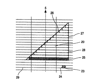
FIG. 2 shows a raster line-shaped beam formed using an apparatus and writing
2 o strategy of an embodiment of the present invention. Line-shaped beam 25 is
shown moving
in scan direction 5 over a writing pixel grid 29. Each unit or writing pixel
24 of writing pixel
grid 29 is an array of smaller address elements 23. Line-shaped beam 25
exposes all or parts
of a number of writing pixels 24 to compose feature 20. Thus as sloped edge 26
approaches
vertical edge 27, the origin and length of subsequent line shaped flashes 28
are changed. As
will be discussed in detail, in practice line shaped beam flash 25 can be
advantageously
modified to expose feature 20 with resolution comparable to the writing
strategies of FIGs. 1 a
or 1 b and throughput higher than the strategies of FIGs. 1 b or 1 c.
FIGs. 3a, 3b and 3c illustrate a typical example of grids, scan fields and
data fields
used to compose a pattern using an embodiment of the present invention. In
FIG. 3a a writing
CA 02316302 2000-06-23
WO 00/25343 PCT/US99/22221
-11-
pixel 24 is shown overlying address grid 22. As shown, writing pixel 24
consists of an array
of address elements 23 overlaid on address grid 22. Address elements 23 range
in size from
approximately 5 to 20 nanometer (nm) squares and are the basic building block
upon which
pattern feature 20 (FIG. 2) is composed and pattern edges 25 and 27 (FIG. 2)
are placed. As
depicted, writing pixel 24 is a 4x4 array of address elements 23 and
correspondingly has a size
ranging from 20 to 80 nm squares. In the special case where the lithography
system is a
binary raster scan system, one skilled in the art will realize that writing
pixel 24 is identical to
address element 23. Other numbers of address elements 23 can be used to form a
writing
pixel 24 where appropriate, and these alternate embodiments of writing pixel
24 are
1 o understood to be within the scope and spirit of the present invention. The
4x4 array depicted
in FIG. 3a allows for shifts in pattern edges in single address element 23
increments using
four dose levels specified as in a Graybeam rasterized database.
FIG. 3b shows a rectangular flash origin field 36 having a 1x16 array of
writing pixels
24 overlying writing pixel grid 29. As seen in FIG. 3a, each writing pixel 24
has an array of
15 address elements 23. Flash origin field 36 is oriented having a long axis
orthogonal to
periodic scan direction 5. The origin of line shaped beam flash 25 (not shown)
lies within
flash origin field 36. The 1 x 16 array of writing pixels 24 shown, can range
in size from
approximately 320x20 nm to approximately 1280x80 nm where each writing pixel
24 is
between approximately 20 to 80 nm squares. It is important to realize that
flash origin field
2 0 36 is defined by the writing strategy and apparatus employed, and while a
1 x 16 array is
depicted herein, any other appropriate flash origin field 36 containing more
than one writing
pixel 24 can be advantageously be employed. Flash origin field 36 is fixed
with respect to the
regular periodic grid of the apparatus, and only one line-shaped beam flash
having an origin
within flash origin field 36 can be made per line scan.
25 Turning now to FIG. 3c, scan fields and data fields used to compose a
pattern using an
embodiment of the present invention are shown. As known for the basic raster
beam 10 of
FIG 1 a, stage movement and beam scanning are combined to allow exposure of
each flash
field 36. In embodiments ofthe present invention, the beam is scanned along
scan direction 5
while stage motion is orthogonal along stage direction 40. A scan stripe 42 is
an array of
CA 02316302 2000-06-23
WO 00/25343 PCT/US99/Z2221
-12-
flash origin fields 36 (FIG. 3b) exposed during a scan. While only a single
scan stripe 42 is
illustrated in FIG. 3c, it should be understood that a plurality of stripes 42
form a stripe data
segment 44. Each stripe data segment 44 is defined in scan direction 5 by the
height of scan
stripe 42. In stage direction 40, data segment 44 is defined by the amount of
memory
available for temporary storage of the exposure data. Where each flash origin
field 36 is a
1x16 array of writing pixels 24, scan stripe 42 is typically 8192 flashes or
pixels in scan
direction 5, requiring scan amplitudes ranging from approximately 164 to 656
microns (gym).
Where sixteen megabytes of temporary data storage is available, stripe data
segment 44 would
contain approximately 400 scan stripes 42 to define the dimension of data
segment 44 in the
i o direction of stage direction 40..
As depicted, stripe data segment 44 has fringes or segment overlap regions 49.
A
portion of segment overlap 49 is shown overlying an adjacent stripe data
segments 50 and 52.
The overlap of adjacent data segments 50 allow a figure or microcell field 47
to be composed
within either data segment 44 or 50. Microcell field 47 is a figure that was
described in the
1 s previously discussed intermediate data base as being a polygon or group of
polygons having a
size limited to fit within overlap regions 49. Each microcell field 47 has an
origin 41. The
position of microfield 47 is then described by a figure origin vector 46 which
relates origin 41
to figure origin field 48 and stripe data segment 44 as depicted. Where origin
41 is within
figure origin field 48, microcell 47 is entirely exposed by scan stripe 42 of
stripe data segment
zo 44. However, where origin 41 is within a portion of segment overlap 49, for
example that
segment overlap 49 that overlies adjacent data segment 50, microcell 47 is
entirely exposed by
a scan stripe (not shown) of data segment 50. Figure or microcell 47 never has
to be exposed
using flashes in two different scan stripes 42. In this manner, embodiments of
the present
invention advantageously write or expose a pattern without regard for stripe
boundaries. The
25 possibility of exposing different parts of critical features or microcells
47 in different scan
stripes 42 is avoided and stripe butting errors are reduced.
Turning now to FIG. 4, extension of the principle illustrated in FIG. 3c is
shown. An
expanded figure origin data field 54 is shown to include a region wider than
the maximum
range of scattering and resist heating interactions for stripe data segment
44. Using data from
CA 02316302 2000-06-23
WO OOI25343 PCT/US99/22221
-13-
expanded figure origin data field 54, some embodiments of the present
invention can calculate
corrections for proximity effects during run-time in the manner of
aforementioned related
application "METHOD AND APPARATUS FOR RUN-TIME CORRECTION OF
PROXIMITY EFFECTS IN PATTERN GENERATION", Attorney Docket No. M-4459.
s While dose data for all flashes that can influence flashes within data
segment 44 are included
within expanded data field 54, it should be realized that only flashes
required for figures 47
having origin 41 within figure origin field 48 are exposed within stripe data
segment 44.
The beam is scanned in a stepwise, periodic manner, essentially pausing at
each figure
origin field 36 (FIG. 3b) for a fixed flash cycle time using the combined
action of an analog
i o magnetic scan and a retrograde electrostatic scan. Some embodiments of the
present
invention create a staircase deflection trajectory 64 as shown in FIG. 5.
Analog wide field
scan 60 is plotted showing amplitude or y-position versus time The amplitude
of analog scan
60 is typically 8192 writing pixels or approximately 164 to 656 Vim. A high
speed sawtooth
scan 62 having an amplitude of one writing pixel and of a period equal to one
flash cycle
(typically 10 nanosecond for a flash rate of 100 MHz) is superimposed upon
analog scan 60.
The effect of these two deflections combines to create staircase deflection
trajectory 64 which
results in the stepwise, periodic scan described.
Where a line shaped beam is employed, when each scan is complete, one of two
things
happens. If all the necessary flashes within scan stripe 42 (FIG. 3c) are
exposed, the beam
2 o advances the length of one flash origin field (FIG. 3b) and another scan
begins. If the feature
or pattern requires more than one shaped beam exposure within any flash field,
the entire scan
is retraced. During retrace, any remaining flashes are exposed and the beam
advances once all
remaining flashes are completed. This retrace feature of the writing strategy
of the present
invention is only necessary when an x-axis period between any two features in
a scan line is
25 less than the length (typically 16 writing pixels) of flash origin field 36
(FIG. 3b). As an
alternative to retracing scans, retrograde sawtooth scan 62 can be used to
hold the beam for
two or more cycles at any flash field 36 (FIG. 3b). However, repeated use of
this "error
correction" alternative along a given scan would build up cumulative error and
eventually
detract from the advantages of a periodic scan.
CA 02316302 2000-06-23
WO 00/25343 PCT/US99/22221
-14-
Still referring to FIG. 5, it has also been found that employing a staircase
deflection
trajectory is advantageous for a raster scanned Gaussian beam (See, Collier
and Abboud).
Thus, introduction of a small amplitude, high frequency sawtooth signal, for
example
sawtooth scan 62, having the appropriate amplitude and frequency, superimposed
on the main
raster scan 60, can create such a staircase deflection trajectory 64. For a
Gaussian beam, such
as beam 10 of FIG. 1 a, each "stair step" of deflection trajectory 64 has a
width essentially
equal to the pixel spacing. Typically beam diameter is defined as the size of
a pixel. Thus,
unlike previously known methods for employing Gaussian beams, (See, Collier
and Abboud)
the Gaussian beam of the present invention is essentially held steady relative
to the substrate
during each exposure. For example, where raster scan 60 has a width of between
approximately 100 microns to 1 millimeter during which 8192 pixels are
written, an
appropriate high frequency is approximately 8192 times the raster scan
frequency. An
appropriate small amplitude for this frequency is 118192 of the raster scan
amplitude. Thus,
in a typical application, the appropriate high frequency is roughly between
100 megaHertz
15 (MHz) to 1 gigaHertz (GHz) and the appropriate small amplitude roughly 5 to
500 nm. In this
manner, the asymmetry in critical dimension values caused by differences in
the slope of the
edges of energy profiles in the resist is reduced or eliminated.
The fundamental frequency of sawtooth scan 62, the fundamental through the
third
harmonic, or other higher order harmonic summations of sawtooth 62 are used to
approximate
2 o the appropriate retrograde scan needed according to the well-known Fourier
series for a
sawtooth waveform. Since the Fourier expansion of sawtooth waveforms is a
rapidly
converging, alternating series, it is possible to use a band-limited function
generator for
creating the sawtooth. In addition, as the main error of approximation is
concentrated in the
first (and last) half cycle of the highest frequency term included in the
approximation,
25 blanking during this time advantageously eliminates most of the error. Thus
for a 100 MHz
pixel cycle, a three-term approximation to the sawtooth wave directs a 30
nanosecond (ns)
blank time and a 70 ns exposure time. As it can be seen, advantageously this
method directs
times that are both practical and readily implementable. In one advantageous
embodiment of
the present invention, the retrograde scan is generated employing a fast
digital to analog
CA 02316302 2000-06-23
WO 00/25343 PCTNS99/22221
-15-
converter (DAC), operating at N times the pixel frequency, and a smothing
filter. N is a small
integer greater than 1 and is typically equal to 3.
It will be understood that the Gaussian beam having a staircase deflection
trajectory of
the present invention is only essentially held steady relative to the
substrate during exposure.
That is to say, that there is some relative movement and hence some slight
beam smearing
along the scan axis. However, by choosing the appropriate sawtooth 62, beam
smearing can
be minimized. Thus for the case of an 80 nm Gaussian beam that employs a 30 ns
blank time
and a 70 ns exposure time, the edge width of a feature without retrograde
scanning is
approximately 120 nm. Where the fundamental (sine wave) approximation for a
retrograde
1 o scan is used, this edge width is reduced to approximately 84 nm and where
a three-term
approximation is used, the edge width is further reduced to approximately 80
nm.
Turning now to FIGs. 6a and 6b, alternate pattern exposure embodiments
employing
line shaped beams are shown. Either embodiment advantageously allows pattern
data to be
composed on the finer resolution of address grid 22 (FIG. 3a). In FIG. 6a, an
origin 71 of line
shaped beam 70 is shown positioned at a distance from origin 72 of flash
origin field 36. This
distance and direction of displacement are indicated by flash origin vector
73. Line shaped
beam 70 is represented in FIG. 6a as equal in length to that of flash origin
field 36. However,
length 74 of shaped beam 70 can be any number of address elements 23 between 0
and the
full length of flash origin field 36, in this case 64 address elements 23. It
has been found
2 o desirable in some embodiments of the present invention to have flash
origin fields 16 writing
pixels long, although other appropriate lengths can be used, for example 8
writing pixels.
When line shape origin 71 is displaced from field origin 72, the position and
length of line
shaped beam 70 is adjusted in address unit increments. In the embodiment of
FIG. 6a, the
origin 71 of line shaped beam flash 70 is deflected from origin 72 of flash
origin field 36
25 using very low amplitude 0 to 64 address unit "microvector" deflections
along the x axis and 0
to 4 address unit "microvector" deflections along the y axis. Position of line
shape origin 71
and length 74 of shaped beam 70 can be changed between each flash cycle.
FIG. 6b shows another pattern exposure embodiment where Graybeam flash duty
cycle modulation is used for positioning figure edges (not shown). As
discussed with respect
CA 02316302 2000-06-23
WO 00/25343 PCT/US99/22221
-16-
to FIG. 6a, length 74 of the line shape beam 70 can range from, for example, 0
to 16 pixels or
0 to 64 address units. Origin 71 can be deflected in one address unit steps to
any of 64 sites
along the x axis. In the embodiment of FIG. 6b, four different dose levels 78
(indicated here
by cross hatching) shifts edges in one address increment steps along the y
axis using
Graybeam methods.
In both FIG. 6a and 6b, it should be noted that line shaped beam 70 can expose
pixels
in an adjacent flash field 77. While these pixels in adjacent field 77 can
alternately be
exposed in a subsequent scan, embodiments of the present invention
advantageously expose
them in this scan. Thus, a sixteen writing pixel flash length and sixteen
pixel origin
1 o microvectoring allow exposure of any sixteen of the thirty-two possible
writing pixel sites in
the two adjacent flash fields 36, 77. This overlapping of scan line exposures
is a feature of
embodiments of the present invention that effects throughput and accuracy.
Eliminating hard
scan line boundaries avoids partial exposures of narrow features allowing
features to be
composed with fewer flashes. For example, if flash 70 had to remain within the
boundaries of
the flash origin field 36, equal line and space periods of less than 64
address units would often
require retrace scans. When flash 70 is allowed to extend into adjacent flash
field 77, all line
and spaces periods greater than 128 address elements are composed without
retrace,
regardless of the relationship between flash origin field grid 36 and pattern
detail. Thus the
overlapping field procedure of embodiments of the present invention allow for
composing
2 o patterns with line shapes at a coverage rate up to twice as high as a non-
overlap procedure.
Any data path that can supply the necessary shape length, microvector position
and
dose data required to specify each flash can be used in the embodiments of the
present
invention. However, raster shaped beam strategy is particularly effective when
used in
conjunction with high speed raster scan data path electronics that generate
rasterized data by
parallel processing. For example, US Patents 4,806,921 and 4,879,604 ATEQ /
Etec assigned
to the same assignee and incorporated by reference herein, are examples of
parallel processing
rasterization data paths originally intended for multiple Graybeam systems
that can be adapted
or easily modified to control a line shaped beam of an embodiment of the
present invention as
described herein.
CA 02316302 2000-06-23
WO 00/25343 PCTNS99/22221
-17-
A rasterized data base specifies a binary or graylevel dose for each writing
pixel 24
(FIG. 3c) in the pattern. This data is generated in run time and temporarily
stored in a pixel
data buffer. Where line shaped beams are employed, the pixel data buffer
contains all the data
for one stripe data segment 44 (FIG. 3b). The raster shaped beam (RSB)
strategy requires
s flash data specifying origin position 71 (FIG. 6a) of flash 70 (FIG. 6a)
within flash origin field
36 (FIG. 6a), length 74 (FIG. 6a) of flash 70, and dose. In the lx 16 pixel
flash field 36 of
FIG. 6a, the data for overlapping line shaped flashes is derived from a row of
thirty-two side
by side writing pixels. Data for sixteen pixels within the current flash
origin field is updated
each flash cycle, while data for sixteen pixels in the adjacent flash field is
obtained by
1 o modifying data loaded during the previous scan.
FIG. 7 shows a block diagram for an embodiment of a decoder that reduces
rasterized
data to line shaped beam microvector data. In the example of this embodiment,
suited for 16
x 1 pixel flash fields and binary dose levels, input to the decoder is binary
dose data for
groups of sixteen side by side writing pixels. The binary dose data is stored
in pattern buffer
1 s memory 80 in columns containing the data for sixteen pixel flash fields in
first scan line 82
depicted between scan line grid boundaries 83, and in an adjacent second scan
line 84. Data
for scan lines 82 and 84 are read out sequentially. A typical bit map
configuration for two
adjacent flash fields is shown with the exposed pixels cross hatched marked
for clarity.
Data is extracted from pattern buffer memory 80 in groups of sixteen writing
pixels
2 o per flash. To begin the cycle that will compose origin and shape length
data for scan field 82,
data for the adjacent scan field 84 is read from buffer 80 and loaded into
processor 86.
Processor 86 counts the number of successive exposed pixels starting from the
point adjacent
scan field 82. This data will be used later to determine overlapping flash
length.
Modified pixel data field 87, that has been read from scan field 82 in the
previous scan
25 cycle and stored for one scan line cycle, is moved from a shift register 88
into a processor 90.
Processor 90 counts the number of successive unexposed pixels starting from
the point
adjacent scan field 85. This data is the deflection of the origin of the line
shaped beam or
flash in that flash field. Processor 90 also counts the number of successive
exposed pixels
(cross hatched marked for clarity) after an edge 89 that is the boundary
between exposed and
CA 02316302 2000-06-23
WO 00/25343 PC'f/US99/22221
-18-
unexposed pixels. This count data is transferred to processor 86, and added to
the output of
processor B to determine the length of the flash. If the flash ends in scan
field 82, the output
of processor 86 is zero. If the flash doesn't end in scan field 82, the sum of
pixels can be
either greater than or less than sixteen. When the sum of pixels is less than
sixteen, all
s exposed pixels in scan field 84 are included in the flash having an origin
in scan field 82.
When the sum of pixels is greater than sixteen, then the pixels in excess of
sixteen that are in
scan field 84 to create a new flash with a new origin. 'Thus modified output
data is loaded into
the shift register 88 containing only those pixels in scan field 84 that need
to be exposed.
In the next flash cycle, exposed pixels are erased (set to zero) in processor
86 and a
to modified set of pixel data transferred to shift register 88 for temporary
storage. This modified
data emerges one scan line later to be inserted into processor 90 during the
next scan cycle.
This cycle continues until all scan lines in buffer 80 have been exposed. In
the meantime, a
second buffer (not shown) is being refilled from the parallel processors
creating rasterized
data, allowing data segments to be exposed without interruption.
15 Lookup table 92 is loaded with calibration data 94 specifying deflections
and blanker
cycles appropriate for the resist process and patterning task. Flash data is
expressed in
dimensionless multiples of address units, and dimensionless fractions of
nominal dose to
simplify calculations. Calibration data 94 is then used to convert
dimensionless data to
microvector deflections, shaper deflections needed to compose the pattern, and
the flash duty
2 o cycles necessary to expose it properly.
The result of the calculation of scan origin and flash length is used as
address data 93
for lookup table 92 that provides an output for deflection and shaping. Thus
flash 98 has an
origin 100, a length 102 and a dose 104 generated in the manner described.
Provided the entire wide field scan and feature composition grid structure
(FIG. 3) is
25 scaled together, (i.e. is based upon multiples of a single specified
address unit), a
dimensionless rasterized data base may be used for different sized patterns.
Using lookup
table 92 to convert from address units to deflection distances at the end of
the data path
advantageously adds scaling capability to the data path.
CA 02316302 2000-06-23
WO 00/25343 PCT/US99/22221
-19-
Those familiar with raster scan data path design will recognize that other
decoder
principles could be applied. For example, decoders can be devised to process
Graylevel
pattern representations using finer address structure. Such a decoder
generates dose as well as
origin and length vectors to position edges on an address structure smaller
than the writing
pixel.
Where embodiments of the present invention are employed for electron beam
lithography systems, electron optics supporting the line shaped beam strategy
are beneficial to
achieve high performance. As known, a shaped electron beam lithography column
typically
consists of an electron gun, intermediate beam shaping optics, a
demagnification lens, and an
overlaid objective lens and wide field deflection system. Provision for
turning the beam on
and off (blanking) for all or part of the flash cycle is also typically
required. In embodiments
of the RSB writing strategy of the present invention, a line shaped beam
having the proper
length and origin position will be formed at very high speed using small
microvector
deflections. Blanking should be capable of modulating dose during very short
flash times
1 s characteristic of embodiments of the RSB strategy. In addition, high
current density is needed
to support the flash rates possible with embodiments of the present invention.
FIG. 8 is a schematic drawing of a typical prior art variable shaped beam
electron
optics column specialized for vector scan writing strategy. A thermionic
electron gun 110
illuminates a square upper shape aperture 112, whose image or shadow is
projected upon a
2o similar square lower shape aperture 114. The image of the upper shape is
deflected by a two
axis electrostatic deflector 116. After a demagnification lens 118, the image
of the shape is
deflected by wide field magnetic deflection coils 120, and subfield
electrostatic deflectors 122
within the objective lens 124. Using very fast electrostatic deflectors 126,
the beam may be
blanked above the first shape. Two additional field lenses 128 are used to
place images of the
2 5 gun crossover at desired locations along the beam axis. There are other
prior art column
configurations that image the gun crossover instead of shape apertures. These
optics often use
thermal field emission (TFE) electron guns, and are specialized for raster or
vector scan
writing strategies using a Gaussian (as opposed to shaped) beam.
CA 02316302 2000-06-23
WO 00/25343 PCTNS99/22221
-20-
With the exception of wide field magnetic deflection optimized for raster
scan, and
very fast low voltage subfield deflections, the lower column optics
configuration of an RSB
optimized column is similar to FIG. 8. However, the middle and upper column
optics are
modified from that shown in FIG. 8 to support a high flash rate.
s FIG. 9 shows a schematic of upper column optics modified for embodiments of
the
RSB writing strategy of the present invention. Raster shaped beam strategy
requires a very
small one axis variable shaped beam with very high current density. The upper
column optics
include a thermal field emission (TFE) electron gun 130, within which a square
upper shape
aperture 132 casts a shadow image that forms a well defined illuminating beam
because the
1 o brightness and associated depth of field of TFE illumination is favorable.
Below the gun is a
collimator lens 134 which projects a shadow of the gun aperture upon a
rectangular line shape
aperture 136. Passing through a field lens 146 at the plane~of the lower
shape, the beam enters
the pupil of a demagnification lens 138, and into the objective lens optics
shown in FIG. 8.
A strong quadruple stigmator 140 is located within or above the collimator
lens 134.
1 s In this manner, the lens is stronger in the long axis of the lower shape,
and weaker in the short
axis of the lower shape. Using stigmator 140, two astigmatic crossovers 142,
144 or line
images of the TFE cathode in gun 130 are formed, and the beam illuminating
rectangular
lower shape aperture 136 is a rectangular shadow 145 of the gun aperture 132.
After passing
through the shape and field lens 146, the beam uniformly fills the
demagnification lens pupil
20 138 as required to minimize lens aberrations and beam interactions effects
in the objective
lens.
As known, emission from a TFE cathode (not shown) is only uniform over a
limited
angle. The upper column embodiment of FIG. 9 optimally uses current passing
through upper
shape aperture 132, maximizing current while minimizing angle of emission and
angular
2 s intensity needed from the cathode. Thus, beam current higher than
otherwise possible is
provided without compromising either uniformity of shape illumination or edge
resolution of
the line shape.
In addition, it is known that electron - electron or beam interactions in the
upper
column can be a serious limitation in field emission optics. Astigmatic
illumination of
CA 02316302 2000-06-23
WO 00/25343 PCT/US99/22221
-21-
embodiments of the upper column optics of the present invention minimize such
beam
interactions through more efficient use of beam current. Relatively little
current is lost on
lower shape aperture 136. There are no fully focused crossovers with that
could cause
excessive energy spread in the beam.
FIG. 10 illustrates leveraged co-planar blanking and shaping of embodiments of
the
present invention. In a line shaped beam, height (narrow axis dimension) of
the shape is
determined by the fixed width of shape aperture 136. As described, RSB writing
strategies
only shape the beam in its long axis. This shaping can be performed by
deflecting rectangular
shadow of the gun aperture 145 (FIG. 9) to position 152 along the long axis of
the shape
to aperture. Orthogonal deflection axis 150 may be used for blanking the beam
without
influencing either its length or width by deflecting it to position 154. Thus
shaping and
blanking are co-planer.
Electrostatic shaping deflectors 156 and electrostatic shaping blanking
deflectors 158
are located above collimator lens 134. The focal length of collimator lens 134
is short enough
1 s to magnify the angular deflection of the deflectors. Along with the
terminated strip line
configuration of the deflectors 156, 158 this leveraging method of the present
invention,
allows for low voltage, very high speed deflection to support high flash rates
used in
embodiments of the RSB writing strategy of the present invention.
While some of the embodiments of the present invention have been described in
terms
2 0 of electron beam lithography, it should be realized that the principles of
the writing strategy
described, including the electron optical column modifications and
enhancements can be used
in light optical or other charged particle lithography systems. The scope and
spirit of the
present invention anticipates such use and therefore includes any light
optical or other particle
beam application that make use of the teachings and disclosures contained
herein.