Note: Descriptions are shown in the official language in which they were submitted.
CA 02316514 2000-10-06
CROSSTALK ELIMINATION METHOD AND SYSTEM
BACKGROUND OF THE INVENTION
1. Field of the invention
The present invention relates to a crosstalk elimination
method and system for use in a transmission system that transmits
a plurality of pairs of a data signal and a clock signal thereof .
2. Description of the Related Art
In the case of a plurality of transmission lines that are
close together, crosstalk occurs when magnetic fields or current
from nearby transmission lines interrupt electrical currents in
a transmission line. Since crosstalk causes data error and
transmission error, it is very important to effectively eliminate
crosstalk from the transmission system.
A simple but effective crosstalk elimination method is to
transmit a plurality of pairs of data and clock signals through
different cables . Since the pairs of data and clock signals are
properly separated from each other, such a conventional system
effectively eliminates crosstalk even in the case where these data
signals are not synchronized.
However, the conventional transmissionsystem needs as many
cables as the pairs of data and clock signals . Therefore , laying
cables should be done with caution not to generate crosstalk,
CA 02316514 2000-10-06
FQ5-485 2
resulting in difficult pattern design. Further, it is difficult
to achieve a downsizing of transmission equipment in the case where
a large number of pairs of data and clock signals.
SUMMARY OF THE INVENTION
An object of the present invention is to provide crosstalk
elimination method and system allowing the reduced number of
cables and a downsizing of transmission equipment.
Another object of the present invention is to provide
crosstalk elimination method and system allowing a stable and
reliable transmission system with simplified cabling.
According to the present invention, a system for
eliminating crosstalk among a plurality of data signals traveling
from sending equipment to receiving equipment through a
transmission cable. Clock signals each associated with the data
signals are not synchronized with each other.
The sending equipment includes a detector for detecting a
possible crosstalk timing in each of the data signals by comparing
phases of the clock signals to transmit it to the receiving
equipment. The receiving equipment includes a read timing
shifter for shifting a read timing of each of the clock signals
associated with a corresponding data signal to a no-crosstalk
timing determined based on the possible crosstalk timing.
The detector may include: a leading edge detector for
CA 02316514 2000-10-06
FQ5-485 3
detecting a leading edge timing of each of the clock signals; a
trailing edge detector for detecting a trailing edge timing of
the clock signal; and a crosstalk timing detector for detecting
the possible crosstalk timing in a corresponding data signal based
on the trailing edge timing of the clock signal associated with
it and leading edge timings of all clock signals other than the
clock signal.
The receiving equipment may further include: a first data
reading section for reading each of the data signals received from
the sending equipment according to the no-crosstalk timing to
produce a first data signal; and a second data reading section
for reading the first data signal according to the read timing
of a corresponding clock signal.
As an embodiment of the present invention, the sending
equipment may include a phase comparator for comparing phases of
the clock signals to produce a phase shift trigger signal
indicating a possible crosstalk timing for each of the data signals ,
to transmit the phase shift trigger signal to the receiving
equipment. The receiving equipment may include: a read timing
shifter for receiving the phase shift trigger signal and a
corresponding clock signal and shifting a read timing of the
corresponding clock signal depending on the phase shift trigger
signal to produce a shifted read timing signal; and a data reading
section for receiving the data signal, the corresponding clock
signal, and the shifted read timing signal, and reading the data
signal according to the shifter read timing signal to produce a
CA 02316514 2000-10-06
FQS-485
first data signal and thereafter reading the first data signal
according to the corresponding clock signal to produce a final
data signal.
The phase comparator may include : a leading edge detector
for detecting a leading edge timing of each of the clock signals ;
a trailing edge detector for detecting a trailing edge timing of
the clock signal; a crosstalk timing detector for detecting the
possible crosstalk timing in a corresponding data signal based
on the trailing edge timing of the clock signal associated with
it and leading edge timings of all clock signals other than the
clock signal; and a trigger generator for generating the phase
shift trigger signal from the possible crosstalk timing, wherein
the phase shift trigger signal has a pulse width having the
possible crosstalk timing located therein.
The read timing shifter may inlcude a selector for selecting
one of the corresponding clock signal and a fixed signal being
a logic high level depending on the phase shift trigger signal,
wherein the corresponding clock signal is selected when the phase
shift trigger signal is a logic low level and the fixed signal
is selected when the phase shift trigger signal is a logic high
level.
The data reading section may include a first flip-flop
circuit for reading the data signal according to the shifted read
timing signal to produce the first data signal; and a second
flip-flop circuit for reading the first data signal according to
the corresponding clock signal.
CA 02316514 2000-10-06
FQ.'i-485
As described above, according to the present invention,
crosstalk among a plurality of data signals can be effectively
removed. Therefore, a reliable and stable transmission system
can be achieved. Further, the plurality of data signals can be
transmitted as a bundle through a single cable, resulting in the
reduced number of cables and a downsizing of the transmission
system. This causes the design of cabling to be simplified and
its cost to be reduced.
BRIEF DESCRIPTION OF THE DRAWINGS
Fig. 1 is a block diagram showing a transmission system
employing a crosstalk elimination system according to an
embodiment of the present invention;
Fig. 2 is a schematic block diagram showing a phase
comparator used in the embodiment of Fig. 1;
Fig. 3 is a time chart showing a first operation of the
embodiment;
Fig. 4 is a time chart showing a second operation of the
embodiment;
Fig. 5 is a detailed block diagram showing a phase comparator
CA 02316514 2000-10-06
FQ 5-485
used in the embodiment of Fig. 2;
Fig. 6 is a time chart showing an operation of the phase
comparator of Fig. 5;
Fig. 7 is a detailed block diagram showing phase shifters
used in the embodiment of Fig. 2;
Fig. 8 is a time chart showing an operation of the phase
shifters of Fig. 7;
Fig. 9 is a detailed block diagram showing data reading
sections used in the embodiment of Fig. 2; and
Fig. 10A and lOB are time charts showing respective
operations of the data reading sections of Fig. 7.
DETAILED DESCRIPTION OF THE PREFERRED EMBODIMENTS
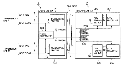
Referring to Fig. 1, it is assumed for simplicity that a
transmission system is composed of a sending system and a receiving
system 2 , which are connected by a single cable 301. The sending
system 1 receives a plurality of pairs of data and clock signals,
which are not synchronized to each other.
Here, the sending system 1 includes a transmission section
CA 02316514 2000-10-06
FQ5-485
101 , a transmission section 102 , and a phase comparator 103 . The
sending system 1 receives a first pair of a data signal 3 and a
clock signal 4 through a first transmission line and a second pair
of a data signal 5 and a clock signal 6 through a second
transmission line.
The transmission sections 101 and 102 receive the input data
signals 3 and 4 and clock signals 11 and 12 that are received from
the phase comparator 103, and transmits a pair of a data signal
7 and a clock signal 8 corresponding to the first pair and a pair
of a data signal 9 and a clock signal 10 corresponding to the second
pair.
The phase comparator 103 compares the clock signals 4 and
6 to produce monostable trigger signals 13 and 14 each indicating
possible crosstalk timings , at which crosstalk may be generated
at the receiving system 2. More specifically, the trigger signal
13 indicates the timing of possible crosstalk from the data signal
9 to the data signal 7 and the trigger signal 14 indicates the
timing of possible crosstalk from the data signal 7 to the data
signal 9. The details of the phase comparator 103 will be
described later.
The sending system 1 transmits a pair of the data signal
7 and the clock signal 8 , a pair of the data signal 9 and the clock
signal 10, and the trigger signals 13 and 14 to the receiving system
2 through the cable 301. Here, the clock signals 4 and 6 are not
synchronized and both clock frequencies are low. The clock
signals 8 and 10 are also not synchronized and both clock
CA 02316514 2000-10-06
FQ5-485
frequencies are low.
The receiving system 2 includes data processors 201 and 202 ,
phase shifters 203 and 204 , and data reading sections 205 and 206 .
The phase shifter 203 receives the clock signal 8 and the trigger
signal 13 indicating the timing of possible crosstalk from the
data signal 9 to the data signal 7. When the trigger signal 13
is output, the phase shifter 203 shifts the phase of the clock
signal 8 to the timing at which no crosstalk could be generated
to produce a reading clock signal 15. As described later, the
amount of the time shift is determined depending on the pulse width
of the trigger signal 13 . When the trigger signal 13 is not output ,
the phase shifter 203 outputs the clock signal 8 as the reading
clock signal 15. The data reading section 205 reads a first data
signal from the data signal 7 according to the reading clock signal
15 having the timing at which no crosstalk could be generated.
Thereafter, the data reading section 205 further reads a second
data signal 17 from the first data signal according to the clock
signal 8 for synchronization with the clock signal 8.
Similarly, the phase shifter 204 receives the clock signal
10 and the trigger signal 14 indicating the timing of possible
crosstalk from the data signal 7 to the data signal 9. When the
trigger signal 14 is output, the phase shifter 204 shifts the phase
of the clock signal 10 to the timing at which no crosstalk could
be generated to produce a reading clock signal 16. As described
later, the amount of the time shift is determined depending on
the pulse width of the trigger signal 14. When the trigger signal
CA 02316514 2000-10-06
FQ5-485
14 is not output , the phase shifter 204 outputs the clock signal
as the reading clock signal 16. The data reading section 206
reads a first data signal from the data signal 9 according to the
reading clock signal 16 having the timing at which no crosstalk
5 could be generated. Thereafter, the data reading section 206
further reads a second data signal 18 from the first data signal
according to the clock signal 10 for synchronization with the clock
signal 10.
The respective data processor 201 and 202 process the data
10 signals 17 and 18 output from the data reading sections 205 and
206.
Referring to Fig . 2 , the phase comparator 103 is provided
with a trailing edge detector 104 and a leading edge detector 105 ,
which detect the trailing edges and leading edges of the clock
signal 4, respectively, and a trailing edge detector 106 and a
leading edge detector 107, which detect the trailing edges and
leading edges of the clock signal 6 , respectively. The trailing
edge timing of the clock signal 4 detected by the trailing edge
detector 104 and the leading edge timing of the clock signal 6
detected by the leading edge detector 107 are output to a crosstalk
timing detector 108. The trailing edge timing of the clock signal
6 detected by the trailing edge detector 106 and the leading edge
timing of the clock signal 4 detected by the leading edge detector
105 are output to a crosstalk timing detector 109.
In the present embodiment, a data signal changes in
synchronization with the trailing edge timing of its clock signal.
CA 02316514 2000-10-06
FQ'.i-485 1 0
Therefore, when one of the clock signals 4 and 6 goes low before
and after the other goes high, crosstalk is likely to occur. The
crosstalk timing detector 108 detects a possible crosstalk timing
in the data signal 7 to produce the trigger signal 13. Similarly,
the crosstalk timing detector 109 detects a possible crosstalk
timing in the data signal 9 to produce the trigger signal 14.
As described later, each of the trailing edge detectors 104
and 106 and the leading edge detectors 105 and 107 includes a delay
circuit for delaying the corresponding input clock signal by a
predetermined amount. Therefore, the clock signal 4 is delayed
by a delay circuit 110 and the delayed clock signal 11 is output
to the transmission section 101. Similarly, the clock signal 6
is delayed by a delay circuit 111 and the delayed clock signal
12 is output to the transmission section 102. Therefore, the
delayed clock signals 11 and 12 are transmitted as the clock
signals 8 and 10 through the cable 301, respectively.
CROSSTALK ELIMINATION OPERATION
A crosstalk elimination operation in the data signal 7
according to the embodiment will be described with reference to
Fig. 3.
Referring to Fig. 3, it is assumed that the clock signal
4 goes low and the clock signal 6 goes high at time instant t0.
In this case, if no crosstalk elimination were made, then, at the
receiving system 2 , the data signal 7 would be read at the trailing
edge timing t2 of the clock signal 8. However, the trailing edge
timing t2 of the clock signal 8 is also the leading edge timing
CA 02316514 2000-10-06
FQ'.i-485 1 1
of the clock signal 10 corresponding to the clock signal 6.
Therefore, the data signal 9 would interfere with the data signal
7 at the timing t2.
The crosstalk timing detector 108 of the phase comparator
103 detects possible crosstalk timing from the trailing edge
timing 19 of the clock signal 4 detected by the trailing edge
detector 104 and the leading edge timing 22 of the clock signal
6 detected by the leading edge detector 107. The crosstalk timing
detector 108 outputs the trigger signal 13 having a pulse width
(t1-t3) having the trailing edge timing t2 of the clock signal
8 located therein.
At the receiving system 2 , the phase shifter 203 receives
the clock signal 8 and the trigger signal 13. If the trigger signal
13 is in a logic level of "0", then the received clock signal 8
is supplied as a reading clock signal 15 to the data reading section
205 because no crosstalk occurs . If the trigger signal 13 is in
a logic level of "1" , which means that crosstalk may occur, then
the phase shifter 203 shifts the trailing edge of the clock signal
8 to the trailing edge timing of the trigger signal 13 to produce
a reading clock signal 15 as shown in ( c ) through ( a ) of Fig . 3 .
The trailing edge timing of the trigger signal 13 is located before
the corresponding data signal changes. Therefore, the reading
clock signal 15 produced by the phase shifter 203 always has the
read timing at which no crosstalk occurs.
The data reading section 205 reads a first data signal
indicated by reference symbol "A" from the data signal 7 according
CA 02316514 2000-10-06
FQ5-485 1 2
to the timing of the reading clock signal 15 as shown (h) of Fig.
3. Thereafter, the data reading section 205 further reads a
second data signal 17 from the first data signal A according to
the original timing of the clock signal 8 for synchronization with
the clock signal 8 as shown in (i) of Fig. 3.
Next , a crosstalk elimination operation in the data signal
9 according to the embodiment will be described with reference
to Fig. 4.
Referring to Fig. 4, it is assumed that the clock signal
6 goes low and the clock signal 4 goes high at time instant t4.
In this case, if no crosstalk elimination were made, then, at the
receiving system 2 , the data signal 9 would be read at the trailing
edge timing t6 of the clock signal 10. However, the trailing edge
timing t6 of the clock signal 10 is also the leading edge timing
of the clock signal 8 corresponding to the clock signal 4.
Therefore, the data signal 7 would interfere with the data signal
9 at the timing t6.
The crosstalk timing detector 109 of the phase comparator
103 detects possible crosstalk timing from the trailing edge
timing 21 of the clock signal 6 detected by the trailing edge
detector 106 and the leading edge timing 20 of the clock signal
4 detected by the leading edge detector 105. The crosstalk timing
detector 109 outputs the trigger signal 14 having a pulse width
(t5-t7) having the trailing edge timing t6 of the clock signal
10 located therein.
At the receiving system 2 , the phase shifter 204 receives
CA 02316514 2000-10-06
FQ'.i-485 1 3
the clock signal 10 and the trigger signal 14. If the trigger
signal 14 is in a logic level of "0" , then the received clock signal
is supplied as a reading clock signal 16 to the data reading
section 206 because no crosstalk occurs . If the trigger signal
5 14 is in a logic level of "1" , which means that crosstalk may occur,
then the phase shifter 204 shifts the trailing edge of the clock
signal 10 to the trailing edge timing of the trigger signal 14
to produce a reading clock signal 16 as shown in ( c ) through ( a )
of Fig. 4. The trailing edge timing of the trigger signal 14 is
10 located before the corresponding data signal changes . Therefore,
the reading clock signal 16 produced by the phase shifter 204
always has the timing at which no crosstalk occurs.
The data reading section 206 reads a first data signal
indicated by reference symbol "B" from the data signal 9 according
to the timing of the reading clock signal 16 as shown ( h ) of Fig .
4. Thereafter, the data reading section 206 further reads a
second data signal 18 from the first data signal B according to
the original timing of the clock signal 10 for synchronization
with the clock signal 10 as shown in (i) of Fig. 4.
In this manner, crosstalk can be effectively removed from
data signals traveling on the cable 301. Therefore, compared with
the prior art , a plurality of pairs of data and clock signals can
be transmitted through a smaller number of cables.
EXAMPLES
Phase comparator
An example of the phase comparator 103 will be described
CA 02316514 2000-10-06
FQ:i-485 1 4
with reference to Figs. 5 and 6.
Referring to Fig. 5, the phase comparator 103, as described
in Fig. 2, is provided with the trailing edge detector 104 and
the leading edge detector 105, the trailing edge detector 106 and
the leading edge detector 107 , and the delay circuits 110 and 111 .
The trailing edge detector 104 is composed of an inverter
and an AND gate that performs a logical AND operation on the delayed
clock signal 11 and a clock signal obtained by the inverter
logically inverting the clock signal 4 to produce the trailing
edge timing signal 19 of the clock signal 4. The leading edge
detector 105 is composed of an inverter and an AND gate that
performs a logical AND operation on the clock signal 4 and a clock
signal obtained by the inverter inverting the delayed clock signal
11 to produce the leading edge timing signal 20 of the clock signal
4.
Similarly, the trailing edge detector 106 is composed of
an inverter and an AND gate that performs a logical AND operation
on the delayed clock signal 12 and a clock signal obtained by the
inverter logically inverting the clock signal 6 to produce the
trailing edge timing signal 21 of the clock signal 6. The leading
edge detector 107 is composed of an inverter and an AND gate that
performs a logical AND operation on the clock signal 6 and a clock
signal obtained by the inverter inverting the delayed clock signal
12 to produce the leading edge timing signal 22 of the clock signal
6.
The crosstalk timing detector 108 is composed of an AND gate
CA 02316514 2000-10-06
FQ5-485 1 5
and an integrator. The AND gate performs a logical AND operation
on the trailing edge timing signal 19 and the leading edge timing
signal 22 to produce an AND output signal 23. The integrator
performs integration of the AND output signal 23 to produce the
trigger signal 13 having a sufficient pulse width.
The crosstalk timing detector 109 is composed of an AND gate
and an integrator. The AND gate performs a logical AND operation
on the trailing edge timing signal 21 and the leading edge timing
signal 20 to produce an AND output signal 24. The integrator
performs integration of the AND output signal 24 to produce the
trigger signal 14 having a sufficient pulse width.
As shown in Fig. 6, a data signal 3 changes in
synchronization with the trailing edge timing of its clock signal
4. Therefore, when the clock signal 4 goes low (L) just after
the clock signal 6 goes high ( H ) , as indicated by reference numeral
601 , crosstalk from the data signal 9 to the data signal 7 is likely
to occur. As described before, the crosstalk timing detector 108
detects a possible crosstalk timing (AND output 23) in the data
signal 7 to produce the trigger signal 13, which has been widened
by the integrator 108 to cover the possible crosstalk timing.
Similarly, the crosstalk timing detector 109 detects a possible
crosstalk timing (AND output 24) in the data signal 9 to produce
the trigger signal 14 , which has been widened by the integrator
108 to cover the possible crosstalk timing.
Phase shifter
In the receiving system 2 , as described before , the phase
CA 02316514 2000-10-06
FQ5-485 1 6
shifter 203 receives the clock signal 8 and the trigger signal
13 indicating the timing of possible crosstalk from the data signal
9 to the data signal 7. Similarly, the phase shifter 204 receives
the clock signal 10 and the trigger signal 14 indicating the timing
of possible crosstalk from the data signal 7 to the data signal
9.
Referring to Fig. 7, each of the phase shifters 203 and 204
is composed of a selector, which selects one of inputs A and B
depending on a selection signal S and outputs a selected one as
a reading clock signal.
The selector of the phase shifter 203 inputs the clock signal
8 as input A, a fixed signal being a logic state of 1 (high) as
input B and the trigger signal 13 as the selection signal S . When
the trigger signal 13 is a level of 0 (low) , the selector selects
the clock signal 8 to output it as the reading clock signal 15.
When the trigger signal 13 is a level of 1 (high), the selector
selects the fixed signal being a logic state of 1 (high) to output
it as the reading clock signal 15.
Similarly, the selector of the phase shifter 204 inputs the
clock signal 10 as input A, a fixed signal being a logic state
of 1 (high) as input B and the trigger signal 14 as the selection
signal S. When the trigger signal 14 is a level of 0 (low) , the
selector selects the clock signal 10 to output it as the reading
clock signal 16. When the trigger signal 14 is a level of 1 (high) ,
the selector selects the fixed signal being a logic state of 1
(high) to output it as the reading clock signal 16.
CA 02316514 2000-10-06
FQ5-485 1 '7
As shown in Fig. 8, when the clock signal 8 goes low (L)
and the clock signal 10 goes high (H) , as indicated by reference
numeral 801, crosstalk from the data signal 9 to the data signal
7 is likely to occur. Therefore, the crosstalk timing detector
108 produces the trigger signal 13 having a pulse width during
which the possible crosstalk timing 801 is included and outputs
it to the receiving system 2 as shown in (c) of Fig. 8.
The phase shifter 203 receives the clock signal 8 and the
trigger signal 13 from the sending system 1 . If the trigger signal
13 is in a low level "0" , then the phase shifter 203 selects the
received clock signal 8 as a reading clock signal 15 to the data
reading section 205 because no crosstalk occurs. However, if the
trigger signal 13 is in a high level ° 1" , then the phase shifter
203 selects the fixed signal being the logic state of High to shift
the trailing edge of the clock signal 8 to the trailing edge timing
of the trigger signal 13 to produce the reading clock signal 15
as shown in (e) of Fig. 8. Therefore, the reading clock signal
16 produced by the phase shifter 204 always has the reading timing
at which no crosstalk occurs . It is the same with the phase shifter
204.
Data reading.. section
Referring to Fig. 9 , the data reading section 205 is composed
of a first flip-flop circuit 901 and a second flip-flop circuit
902. The first flip-flop circuit 901 inputs the data signal 7
at the input D and an clock signal 25 generated by an inverter
inverting the reading clock signal 15. The second flip-flop
CA 02316514 2000-10-06
FQ5-485 1 8
circuit 902 inputs the output 27 of the first flip-flop circuit
901 and the clock signal 8.
Similarly, the data reading section 206 is composed of a
first flip-flop circuit 903 and a second flip-flop circuit 904.
The first flip-flop circuit 903 inputs the data signal 9 at the
input D and an clock signal 26 generated by an inverter inverting
the reading clock signal 16. The second flip-flop circuit 904
inputs the output 28 of the first flip-flop circuit 903 and the
clock signal 10.
As shown in Fig. 10A, the first flip-flop circuit 901 of
the data reading section 205 reads a first data signal 27 from
the data signal 7 according to the reading clock signal 15. More
specifically, even if a crosstalk noise 1001 is generated by the
data signal 9 , the reading clock signal 15 has the trailing edge
timing 1002 at which no crosstalk could be generated. Therefore,
the first data signal 27 has no crosstalk noise. However, the
first data signal 27 is not synchronized with the original clock
signal 8.
Thereafter, the second flip-flop circuit 902 further reads
a second data signal 17 from the first data signal 27 according
to the clock signal 8 for synchronization with the clock signal
8. In this way, the data signal 17 having no error can be output
to the data processor 201.
As shown in Fig. 10B, the first flip-flop circuit 903 of
the data reading section 206 reads a first data signal 28 from
the data signal 9 according to the reading clock signal 16. More
CA 02316514 2000-10-06
FQ5-485 1 9
specifically, even if a crosstalk noise 1003 is generated by the
data signal 7 , the reading clock signal 16 has the trailing edge
timing 1004 at which no crosstalk could be generated. Therefore,
the first data signal 28 has no crosstalk noise. However, the
first data signal 28 is not synchronized with the original clock
signal 10.
Thereafter, the second flip-flop circuit 904 further reads
a second data signal 18 from the first data signal 28 according
to the clock signal 10 for synchronization with the clock signal
10. In this way, the data signal 18 having no error can be output
to the data processor 202.
In the above embodiment , the case of two pairs of data and
clock signals is described. However, it is apparent that the
present invention can be applied to three or more pairs of data
and clock signals.
It is contemplated that numerous modifications may be made
to the embodiments and implementations of the present invention
without departing from the spirit and scope of the invention as
defined in the following claims.