Note: Descriptions are shown in the official language in which they were submitted.
CA 02316632 2001-08-28
SIGNAL INTERFACE MODULE
Field of the Invention
1 The present invention relates to a light unit operating apparatus.
Specifically, the
2 present invention provides an apparatus and method for interfacing a railway
signal
3 controller with a light unit.
4 Background of The Invention
Colored signal light units are commonly used in railway control systems to
signal
6 the train crews as to route availability and speed requirements in the
forthcoming area
7 of railway track. Typically, incandescent light units are used as the source
of light, with
8 color added by using external colored lenses. However, non-incandescent
light units,
9 such as light emitting diode (LED) light units, are a desirable substitute
as they provide
a longer life, lower power consumption, and better visibility than
incandescent light
11 units. An LED light unit typically consists of a two-wire input, a power
supply and a
12 plurality of LEDs electrically connected in an array.
13 Electrical or electronic controllers housed in bungalows and located
alongside
14 railroad tracks may control many sets of light units, whether incandescent
or LED.
These controllers often employ light unit integrity tests to verify that the
light unit is
16 working, or is able to work when required. Traditionally, these controllers
control and
17 monitor incandescent light units. Traditional signal integrity testing
consists of at least
18 two separate tests performed by the controller. The first test is the cold
filament test
19 (CFT) which is applied to light units that are not currently energized.
This test consists
of pulses, typically less than two milliseconds in duration but repeated
periodically at
WA 544343.8
CA 02316632 2001-08-28
TITLE: SIGNAL INTERFACE MODULE INVENTOR: MOLLET, ET AL
1 intervals of several seconds, which pulse the filament of the unenergized
incandescent
2 light unit. When the controller's test signal detector senses an adequate
current draw
3 during this CFT test pulse, the controller registers that the incandescent
bulb passes
4 the CFT. If the controller does not sense an adequate current draw during
the CFT test
pulse, the controller registers a failed CFT. The controller also performs a
hot filament
6 test (HFT), which is applied to light units that are currently energized.
The HFT
7 provides that the light unit is periodically monitored for adequate current
draw during the
a times that the light unit is supposed to be energized. In the event of a
loss of electrical
s continuity between the controller and the light unit or an open filament in
an
incandescent light unit, both CFT and HFT tests fail.
11 Traditionally, when incandescent bulbs are pulsed with the CFT pulse, the
slow
12 warm-up time of the filament is such that there is no visible light output
as a result of the
13 test. However, light emitting diodes react much faster than incandescent
buibs. When
14 this test pulsing is applied to an LED light unit it may cause a
perceivable visible blink.
Those familiar with the art will appreciate that this unintended blinking is
an
16 unacceptable condition.
17 The present invention allows quick responding non-incandescent light units
to be
1s used interchangeably with, or as replacements for, incandescent light
units. The
19 present invention also allows using the currently employed controllers
utilizing the
standard CFT and HFT processes, yet avoiding any undesirable blinking of the
non-
21 incandescent light units. The present invention further allows this to be
accomplished
22 without losing the ability of both the CFT and the HFT to verify electrical
continuity
23 between the controller and the light unit.
2 WA 544343.8
CA 02316632 2001-08-28
TITLE: SIGNAL INTERFACE MODULE INVENTOR: MOLLET, ET AL
1 Summary of the Invention
2 The present invention overcomes the above mentioned problems and limitations
3 of the prior art devices by providing an apparatus and method to test the
functional
4 status of non-incandescent light units using existing controllers.
One of the preferred embodiments of the present invention includes: receiving
6 circuitry for receiving a test signal intended for transmission to the light
unit and for
7 receiving an energizing signal; circuitry coupled to the receiving circuitry
to shunt the
8 test signal away from the light unit; circuitry for analyzing a response of
the light unit to
s the energizing signal to determine a non-functional light unit state; and
circuitry for
disabling the shunting circuitry upon determination of the non-functional
light unit state.
11 An embodiment may include the suppression of the test signal from
transmission
12 to the light unit.
13 The present invention provides for a signal interface module (SIM) which
14 interfaces a quick responding non-incandescent light unit with a
controller. Use of the
signal interface module allows non-incandescent lights and incandescent bulbs
to be
16 driven and monitored from the same controller interchangeably, with no
changes to the
17 operation of the controller itself.
18 It is desired that the controllers drive and monitor non-incandescent light
units
19 while still performing both cold filament testing, and hot filament
testing. Therefore,
when using a non-incandescent light unit, the cold filament test pulse which
otherwise
21 could cause a visible blink of the non-incandescent light unit is shunted
away from the
22 non-incandescent light unit. A shunt completes the circuit at the SIM
allowing for the
23 detection of current flow at the controller. Thus, the present invention
allows for the
3 WA 544343.8
CA 02316632 2001-08-28
TITLE: SIGNAL INTERFACE MODULE INVENTOR: MOLLET, ET AL
1 non-incandescent light units to be shunted during the CFT, and for no
visible blinking of
2 the non-incandescent light unit to occur, whereas if the controller is
connected directly
3 to incandescent units, the incandescent units will be subject to both cold
filament tests
4 and hot filament tests in the normal manner.
Simply shunting the light unit for the CFT would allow for the controller to
6 continue to send CFT test pulses if the light unit has failed the HFT test.
Therefore, if
7 the non-incandescent light unit is shunted for the CFT, but no other
precautions are
8 taken, a non-functional status of the non-incandescent light unit would
result in
9 alternating status determined at the controller. The HFT would indicate
light unit failure,
and cause the controller to de-energize the failed light unit. The controller
would then
11 revert to CFT of the failed light unit, which may yield a "light unit OK"
status, and allow
12 the controller to again attempt to energize the light unit, repeating the
cycle indefinitely.
13 An objective of this invention is to provide a consistent response to the
controller
14 in the event that the non-incandescent light unit is non-functional. When
the non-
incandescent light unit is functioning properly, the CFT will be shunted
around the non-
16 incandescent light unit when the light unit is de-energized, and the
controller will sense
17 an adequate current flow during the CFT. In the event that the non-
incandescent light
18 unit is not functioning properly, therefore not drawing an adequate current
during the
19 receipt of the energizing signal, the present invention employs a latch to
be set, which
will disable the flow of current during the CFT, causing the controller to
register a failure
21 on the next CFT. Thus, if the light unit is non-functional, the shunt of
the CFT pulse is
22 disabled and the controller will recognize a failed CFT during the next CFT
therefore
23 indicating a failed light unit under the CFT.
4 WA 544343.8
CA 02316632 2008-01-15
This application could be applied to other forms of light unit testing, such
as
testing of automobile traffic signals or harbor traffic signals.
An objective of this invention is to prevent the blinking effect inherent in a
cold
filament test of the non-incandescent light unit.
Another objective of this invention is to maintain the use of or the validity
of the
CFT to verify electrical continuity between the controller and a location
adjacent to
the light unit such as the light unit enclosure, even though the CFT is
shunted around
the non-incandescent light unit. This can be achieved by locating the
invention
adjacent to the light unit such as inside the light unit enclosure. By placing
the
invention near the light unit the CFT signal must travel to the adjacent
location and
return, therefore verifying the integrity of the electrical continuity between
the
controller and the adjacent location.
Another objective of the present invention is to provide for operation of the
non-incandescent light unit testing over a broad range of operating voltages.
Also an objective of the invention is to provide a signal interface unit in
which
the signal interface unit could sense damage of its own circuitry so as to
shut down
in the event of damage to the circuitry.
In a broad aspect, moreover, the present invention provides a method of
testing the functional status of a light unit with a test signal intended for
transmission
to the light unit from a controller having a test signal detector therein, the
method
comprising the steps of: receiving the test signal, shunting the test signal
away from
the light unit, receiving an energizing signal, analyzing a response of the
light unit to
the energizing signal to determine a non-functional light unit state, and
disabling the
shunting step upon the determination of the non-functional light unit state.
In another broad aspect, the present invention provides an apparatus for use
with testing the functional status of a light unit with a test signal intended
for
transmission to the light unit from a controller having a test signal detector
therein,
comprising: circuitry for receiving a test signal; circuitry coupled to the
receiving
circuitry for shunting the test signal away from the light unit; circuitry for
analyzing a
5
CA 02316632 2008-01-15
response to the light unit to an energizing signal to determine a non-
functional light
unit state; and circuitry for disabling the shunting upon determination of the
non-functional light unit state.
The foregoing and other objects of the invention are intended to be
illustrative
of the invention and are not meant in a limiting sense. Many possible
embodiments
of the invention may be made and will be readily evident upon a study of the
following
specification and accompanying drawings comprising a part thereof. Various
features and sub-combinations of the invention may be employed without
reference
to other features and sub-combinations. Other objects and advantages of this
invention will
5a
CA 02316632 2001-08-28
TITLE: SIGNAL INTERFACE MODULE INVENTOR: MOLLET, ET AL
1 become apparent from the following description taken in connection with the
2 accompanying drawings, wherein is set forth by way of illustration and
example, an
3 embodiment of this invention.
4 Description of the Drawings
Preferred embodiments of the invention, illustrative of the best modes in
which
6 the applicant has contemplated applying the principles, are set forth in the
following
7 description and are shown in the drawings and are particularly and
distinctly pointed out
8 and set forth in the appended claims.
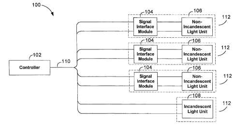
9 Fig. 1 is a simplified block diagram of a train signal controller system
having the
present invention mounted therein.
11 Fig. 2 is a schematic diagram with overlaid phantom line groupings showing
the
12 signal interface module constructed in accordance with a preferred
embodiment of the
13 invention.
14 Fig. 3 is a flow chart showing a test and an energizing signal application
to the
invention.
16 Description of a Preferred Embodiment
17 Referring now to Fig. 1, a railway signal and controller combination 100
18 constructed in accordance with the present invention is illustrated.
Controller 102 is
19 used to monitor and control various devices including signal lights.
Interconnecting
cable 110 is used to connect signal lights, each being in its own enclosure
112, to the
6 WA 544343.8
CA 02316632 2001-08-28
TITLE: SIGNAL INTERFACE MODULE INVENTOR: MOLLET, ET AL
1 controller 102. Traditional systems employ incandescent light units 108 for
the signals.
2 The incandescent light units 108 are wired directly to the controller 102
through cable
3 110. In the present invention, a signal interface module 104 is employed in
4 combination with non-incandescent light unit 106 to provide an apparatus and
method
for testing the functional status of non-incandescent light unit 106 by
receiving and
6 processing signals from a controller 102. The controller could be a solid
state controller
7 such as a Harmon Industries, Inc. Vital Harmon Logic Controller (VHLC),
ElectroCode
8 4, ElectroCode 5, or ElectroLogic 1. A light unit could be a light emitting
diode (LED)
9 unit such as a 45-45263 manufactured by RSO, Inc.
Signal interface module (SIM) 104 includes: receiving circuitry for receiving
a test
11 signal intended for transmission to the light unit and for receiving an
energizing signal;
12 circuitry coupled to the receiving circuitry to shunt the test signal away
from the light
13 unit; suppression circuitry for suppressing the test signal from
transmission to the light
14 unit; circuitry for analyzing a response of the light unit to the
energizing signal to
determine a non-functional light unit state; and circuitry for disabling the
shunting
16 circuitry upon determination of the non-functional light unit state.
17 Referring now to Fig. 2, a preferred embodiment is shown. SIM 104 is
18 connected to controller 102 via interconnecting cable 110 at receiving
terminals 286.
19 SIM 104 is connected to light unit 106 at light unit terminals 288. A cold
filament test
(CFT) emulation circuit 202 shunts the CFT signal away from light unit 106
provided
21 that the light unit has not been previously found to be in a non-functional
state. CFT
22 function latch circuit 210 disables the shunting of the CFT signal away
from the light
23 unit upon determination of the non-functional light unit state. The CFT
emulation circuit
7 WA 544343.8
CA 02316632 2001-08-28
TITLE: SIGNAL INTERFACE MODULE INVENTOR: MOLLET, ET AL
1 is referred to as an emulation circuit because the response of a traditional
light unit
2 having a filament is being emulated by the present invention during the CFT.
In a
3 preferred embodiment, a CFT signal may be a pulse or series of pulses each
of a
4 duration typically less than 2 msec at an amplitude of 11-14 volts. CFT
pulse
suppression circuit 204 adds pulse suppression of the CFT test signal in
addition to the
6 shunt of the CFT test signal. Voltage sense circuit 206 senses for voltage
at the light
7 unit. Current sense circuit 208 senses for current through the light unit.
When the
8 energizing signal is present, CFT function latch circuit 210 analyzes
information from
9 voltage sense circuit 206 and current sense circuit 208 to determine the
functional or
non-functional state of the light unit 106.
11 In more detail, in Fig. 2, CFT emulation circuit 202 shunts the CFT signal
away
U from the light unit. CFT emulation circuit 202 includes diode 212 which
prevents any
13 discharge back from capacitors 216, 218. Capacitor shunt 214 includes
capacitors 216,
14 218, resistors 220, 222 and fuses 224, 226 to provide for the shunt of the
CFT signal.
The capacitors are sized as to shunt the CFT signal received from a specific
controller
16 for the duration of the CFT signal pulse. In a preferred embodiment, diode
212 could
17 be a Fairchild Semiconductor, part number S3M, and capacitors have been
sized to
18 4700 microfarads. Although electrically only one leg of the shunt is
required, two legs
19 are used for a duplicating effect to protect against component failure.
Fuses 224, 226
are present to prevent the controller from viewing the circuit as a closed
loop in the
21 event of a short circuit failure across one or both capacitors. Resistors
220, 222 are 5.6
22 Ohm and fuses 224, 226 are rated at .375 amps in this embodiment.
Serpentine trace
23 228 is wound through the circuitry of SIM 104. In the event of physical
damage to SIM
8 WA 544343.8
CA 02316632 2001-08-28
TITLE: SIGNAL INTERFACE MODULE INVENTOR: MOLLET, ET AL
1 104 and thus serpentine trace 228, the current through CFT emulation circuit
202 will
2 be inhibited due to a loss of conductivity through serpentine trace 228 and
the controller
3 will not detect a proper response to the CFT signal. Serpentine trace 228
could be
4 positioned at other locations in the invention, including in current sense
circuit 208.
Therefore, after determining the existence of circuit damage, the invention
inhibits the
6 shunt. Although, in this embodiment, loss of conductivity through a
conductor indicates
7 circuit damage, circuit damage also can be determined in different ways,
such as
8 current sensing devices.
9 Further in Fig. 2, CFT pulse suppression circuit 204 adds pulse suppression
of
the CFT test signal in addition to the previously discussed shunt of the CFT
signal by
11 CFT emulation circuit 202. The CFT signal is suppressed, but may appear at
the light
12 unit as a reduced voltage pulse. A voltage of less than 2.5 volts is used
in a preferred
13 embodiment. Inductor 232 in combination with resistors 234, 236, 238
perform the
14 suppression function. In a preferred embodiment the inductor is sized to
suppress the
CFT signal to a level below 2.5 volts which is below the activation threshold
of the LED
16 light unit. By the way of example, inductor 232 of pulse suppression
circuit 204 has an
17 inductance of 1.5 Henries with a core material of 80% nickel and 20%
silicon. Inductor
18 232 is designed such that the core saturates after approximately 2 msec of
energizing.
19 This saturation allows for the passage of signals longer in duration than
the 2 msec
CFT signal. Resistors 234, 236, 238 provide for a reset of stored energy in
inductor
21 232 and capacitors 216, 218. To reduce the probability of failure, three
resistors are
22 used instead of one. Although one resistor would electrically be
sufficient, multiple
9 WA 544343.8
CA 02316632 2001-08-28
TITLE: SIGNAL INTERFACE MODULE INVENTOR: MOLLET, ET AL
I resistors are used in this embodiment to avoid failure if one or two should
fail.
2 Preferred resistors include pulse rated metal film resistors of 150 Ohms
each.
3 Voltage sense circuit 206 includes comparator 240 which provides for a
positive
4 output when the output of the signal interface module 104 meets or exceeds a
specified
voltage. In a preferred embodiment this voltage is 8 volts. An example of a
comparator
6 is one of the operational amplifiers on an Analog Devices device, part
number OP491.
7 Voltage sense current 206 includes resistors 242, 244 forming a voltage
divider.
8 Resistors 242, 244 are preferably, 10.0 kOhms and 4.53 kOhms, respectively.
Resistor
9 246 provides a bias current for voltage reference 250 and could be a 10 kOhm
metal
film resistor. Resistor 248 limits the bias current through voltage reference
252.
11 Resistor 248 could also be a 10 kOhm metal film resistor. Precision voltage
reference
12 250 provides a constant voltage at the input of comparator 240, while
precision voltage
13 reference 252 provides for a constant voltage output of comparator 240 when
14 comparator output is in a high state. Precision voltage references 250, 252
in a
preferred embodiment are Motorola, part number LM285, 2.5 VDC.
16 Current sense circuit 208 outputs a voltage proportional to the current
flowing
17 through light unit 106. Resistor 254 is a sensing resistor. A
representative value for
18 resistor 254 is 0.1 Ohm in a preferred embodiment. Resistor 256 is part of
a voltage
19 divider to provide DC offset and could be a 4.99 kOhm resistor. Resistor
258 provides
for a DC offset on the positive input of amplifier 260 in order to raise input
voltage level
21 to amplifier 260 above a noise margin of 25mV. Amplifier 260 is designed in
this
22 embodiment in a non-inverting configuration with a gain of approximately 20
to amplify
23 the voltage across the resistor 254. The output of amplifier 260 is 2.5 VDC
or greater
10 WA 544343.8
CA 02316632 2001-08-28
TITLE: SIGNAL INTERFACE MODULE INVENTOR: MOLLET, ET AL
1 when light unit 106 is functional and energized. Resistors 262 and 264 used
to the set
2 the gain of the amplifier configuration and could be 95.3 kOhms and 4.99
kOhms,
3 respectively. Resistor 258 could be 499 kOhms. Amplifier 260 could be an
operational
4 amplifier in an Analog Devices device, part number OP491.
CFT function latch circuit 210 compares the outputs of voltage sense circuit
206
6 and current sense circuit 208 and disables CFT emulation circuit 202 from
shunting the
7 CFT signal in the event of a non-functioning light unit 106. The non-
functional state of
8 light unit 106 is determined if light unit 106 is receiving a specified
voltage (the output of
9 comparator 240 is high) and inadequate current is flowing through light unit
106 (the
output of amplifier 260 is below the level of a functional light unit). When
these two
11 events co-exist, the output of comparator 266 is high. Resistor 268 and
capacitor 270
12 are part of a delay circuit used to slow down the turn on time of the base-
emitter
13 junction of n-channel BJT transistor 272. A high output on comparator 266
turns on
14 transistor 272. Current fiows through transistor 272 and causes fast acting
fuse 274 to
open. Because fuse 274 is open, MOSFET 276 is not activated during the CFT and
16 does not shunt current. Therefore, CFT emulation circuit 202 is not allowed
to shunt
17 the CFT. Small signal diode pair 280 prevents current through fuse 274
during power
18 up periods of the comparator 266. Resistor 282 limits current to
comparators 240, 266
19 and amplifier 260 in the event of a component short internal to the IC
chip. Resistor
284 limits the current through fuse 274 during the CFT pulse. In a preferred
21 embodiment transistor 272 is an On Semiconductor MMBT3904, MOSFET 276 is a
22 Fairchild Semiconductor IRFW540A, capacitor 270 is 47 microfarads, resistor
282 is
23 243 Ohms, resistor 284 is 51 Ohms and resistor 268 is 1.0 kOhms. Diode pair
280 is
11 WA 544343.8
CA 02316632 2001-08-28
TITLE: SIGNAL INTERFACE MODULE INVENTOR: MOLLET, ET AL
1 an On Semiconductor MMBD7000LT1. An example of comparator 266 is one of the
2 operational amplifiers on an Analog Devices device, part number OP491.
3 As is apparent to one skilled in the art, even in this embodiment,
components
4 could be substituted for those stated. For example, the fast acting fuse
could be
replaced with a resettable device.
6 As is also apparent, the invention could be practiced in many alternative
7 embodiments. For example, a microprocessor or microcontroller could perform
many
8 of the functions of the illustrated embodiment.
9 Also, although a preferred embodiment refers to a CFT signal, a person
skilled in
the art recognizes that the circuit could be configured to recognize many
different
11 varieties of test signals.
12 Also, although a preferred embodiment is shown where LEDs are used for the
13 non-incandescent light units other types of light units could be used.
14 Referring now to Fig. 3, the flow chart shows a CFT and an energizing
signal
applied to signal interface module (SIM) 104. Controller 102 generates signals
that are
16 transmitted to SIM 104. When a CFT signal is being transmitted to SIM 104,
if decision
17 function 318 is not intact, indicating that electrical continuity between
controller 102 and
18 a location, containing at least a portion of SIM 104, adjacent to light
unit 106 is not
19 intact, controller 102 detects a CFT failure.
If electrical continuity between controller 102 and a location, containing at
least
21 a portion of SIM 104, adjacent to light unit 106 is intact, decision
function 318 allows the
22 continued shunt of the CFT signal. In this case, controller 102 detects no
CFT failure
23 and a functional light unit 106.
12 WA 544343.8
CA 02316632 2001-08-28
TITLE: SIGNAL INTERFACE MODULE INVENTOR: MOLLET, ET AL
1 If decision function 304 of CFT emulation circuit 202 (Fig. 2) is "off', the
shunting
2 of the CFT signal away from light unit 106 (Fig. 1) is interrupted and
controller 102
3 detects a CFT failure.
4 If decision function 304 of CFT emulation circuit 202 is "on", function 304
directs
the shunting of the CFT signal away from light unit 106 (Fig. 1). In this
event, controller
6 102 indicates a functional light unit 106 (Fig. 1).
7 Decision function 308 relies upon the intact condition of serpentine trace
228
8 (Fig. 2) to indicate that SIM 104 circuitry is intact. As previously stated,
serpentine trace
s 228 is wound about the circuitry of SIM 104. If serpentine trace 228 is
damaged, it is
likely that SIM 104 circuit components or circuit mounting devices are damaged
11 potentially impairing their proper operation. In such a case, function 308
will inhibit the
12 flow of current during the CFT, causing the controller 102 to register a
non-functional
13 light unit 106.
14 If the serpentine trace is not damaged, function 310 allows the continued
shunt
of the CFT signal away from light unit 106. In this case, controller 102
detects no CFT
16 failure and a functional light unit 106. In this condition, normal
operation of controller
17 102, SIM 104 and light unit 106 continues as shown at function 316.
18 When controller 102 determines a light unit 106 should be illuminated it
transmits
19 an energizing signal to SIM 104. Function 312 analyzes a response of light
unit 106
(Fig. 1) to the energizing signal to determine if light unit 106 is functional
or non-
21 functional. In a preferred embodiment, if comparator 266 finds sufficient
voltage and
22 yet inadequate current at light unit 106, a non-functional light unit
condition is
23 determined. If light unit 106 is determined to be non-functional, function
314 latches
13 WA 544343.8
CA 02316632 2001-08-28
TITLE: SIGNAL INTERFACE MODULE INVENTOR: MOLLET, ET AL
1 CFT emulation circuit 202 (Fig. 2) into an "off' state. By latching CFT
emulation circuit
2 202 to "off," the shunting of the CFT is disabled. This then, changes the
state of
3 function 304 to effect the next CFT signal and indicate light unit failure
at the next CFT.
4 If function 312 determines a functional light unit state, then normal
operation of
controller 102, SIM 104 and light unit 106 continues as shown at function 316.
6 In the foregoing description, certain terms have been used for brevity,
clearness
7 and understanding; but no unnecessary limitations are to be implied
therefrom beyond
8 the requirements of the prior art, because such terms are used for
descriptive purposes
9 and are intended to be broadly construed. Moreover, the description and
illustration of
the inventions is by way of example, and the scope of the inventions is not
limited to the
11 exact details shown or described.
12 Certain changes may be made in embodying the above invention, and in the
13 construction thereof, without departing from the spirit and scope of the
invention. It is
14 intended that all matter contained in the above description and shown in
the
accompanying drawings shall be interpreted as illustrative and not meant in a
limiting
16 sense.
17 Having now described the features, discoveries and principles of the
invention,
18 the manner in which the inventive apparatus is constructed and the method
which is
19 disclosed, the characteristics of the construction, and advantageous, new
and useful
results obtained; the new and useful methods, structures, devices, elements,
21 arrangements, parts and combinations, are set forth in the appended claims.
14 WA 544343.8
CA 02316632 2001-08-28
TITLE: SIGNAL INTERFACE MODULE INVENTOR: MOLLET, ET AL
1 It is understood that the following claims are intended to cover all of the
generic
2 and specific features of the invention herein described, and all statements
of the scope
3 of the invention which, as a matter of language, might be said to fall
therebetween.
15 WA 544343.8
CA 02316632 2001-08-28
SIGNAL INTERFACE MODULE
Field of the Invention
1 The present invention relates to a light unit operating apparatus.
Specifically, the
2 present invention provides an apparatus and method for interfacing a railway
signal
3 controller with a light unit.
4 Background of The Invention
Colored signal light units are commonly used in railway control systems to
signal
6 the train crews as to route availability and speed requirements in the
forthcoming area
7 of railway track. Typically, incandescent light units are used as the source
of light, with
8 color added by using external colored lenses. However, non-incandescent
light units,
9 such as light emitting diode (LED) light units, are a desirable substitute
as they provide
a longer life, lower power consumption, and better visibility than
incandescent light
11 units. An LED light unit typically consists of a two-wire input, a power
supply and a
12 plurality of LEDs electrically connected in an array.
13 Electrical or electronic controllers housed in bungalows and located
alongside
14 railroad tracks may control many sets of light units, whether incandescent
or LED.
These controllers often employ light unit integrity tests to verify that the
light unit is
16 working, or is able to work when required. Traditionally, these controllers
control and
17 monitor incandescent light units. Traditional signal integrity testing
consists of at least
18 two separate tests performed by the controller. The first test is the cold
filament test
19 (CFT) which is applied to light units that are not currently energized.
This test consists
of pulses, typically less than two milliseconds in duration but repeated
periodically at
WA 544343.8
CA 02316632 2001-08-28
TITLE: SIGNAL INTERFACE MODULE INVENTOR: MOLLET, ET AL
1 intervals of several seconds, which pulse the filament of the unenergized
incandescent
2 light unit. When the controller's test signal detector senses an adequate
current draw
3 during this CFT test pulse, the controller registers that the incandescent
bulb passes
4 the CFT. If the controller does not sense an adequate current draw during
the CFT test
pulse, the controller registers a failed CFT. The controller also performs a
hot filament
6 test (HFT), which is applied to light units that are currently energized.
The HFT
7 provides that the light unit is periodically monitored for adequate current
draw during the
a times that the light unit is supposed to be energized. In the event of a
loss of electrical
s continuity between the controller and the light unit or an open filament in
an
incandescent light unit, both CFT and HFT tests fail.
11 Traditionally, when incandescent bulbs are pulsed with the CFT pulse, the
slow
12 warm-up time of the filament is such that there is no visible light output
as a result of the
13 test. However, light emitting diodes react much faster than incandescent
buibs. When
14 this test pulsing is applied to an LED light unit it may cause a
perceivable visible blink.
Those familiar with the art will appreciate that this unintended blinking is
an
16 unacceptable condition.
17 The present invention allows quick responding non-incandescent light units
to be
1s used interchangeably with, or as replacements for, incandescent light
units. The
19 present invention also allows using the currently employed controllers
utilizing the
standard CFT and HFT processes, yet avoiding any undesirable blinking of the
non-
21 incandescent light units. The present invention further allows this to be
accomplished
22 without losing the ability of both the CFT and the HFT to verify electrical
continuity
23 between the controller and the light unit.
2 WA 544343.8
CA 02316632 2001-08-28
TITLE: SIGNAL INTERFACE MODULE INVENTOR: MOLLET, ET AL
1 Summary of the Invention
2 The present invention overcomes the above mentioned problems and limitations
3 of the prior art devices by providing an apparatus and method to test the
functional
4 status of non-incandescent light units using existing controllers.
One of the preferred embodiments of the present invention includes: receiving
6 circuitry for receiving a test signal intended for transmission to the light
unit and for
7 receiving an energizing signal; circuitry coupled to the receiving circuitry
to shunt the
8 test signal away from the light unit; circuitry for analyzing a response of
the light unit to
s the energizing signal to determine a non-functional light unit state; and
circuitry for
disabling the shunting circuitry upon determination of the non-functional
light unit state.
11 An embodiment may include the suppression of the test signal from
transmission
12 to the light unit.
13 The present invention provides for a signal interface module (SIM) which
14 interfaces a quick responding non-incandescent light unit with a
controller. Use of the
signal interface module allows non-incandescent lights and incandescent bulbs
to be
16 driven and monitored from the same controller interchangeably, with no
changes to the
17 operation of the controller itself.
18 It is desired that the controllers drive and monitor non-incandescent light
units
19 while still performing both cold filament testing, and hot filament
testing. Therefore,
when using a non-incandescent light unit, the cold filament test pulse which
otherwise
21 could cause a visible blink of the non-incandescent light unit is shunted
away from the
22 non-incandescent light unit. A shunt completes the circuit at the SIM
allowing for the
23 detection of current flow at the controller. Thus, the present invention
allows for the
3 WA 544343.8
CA 02316632 2001-08-28
TITLE: SIGNAL INTERFACE MODULE INVENTOR: MOLLET, ET AL
1 non-incandescent light units to be shunted during the CFT, and for no
visible blinking of
2 the non-incandescent light unit to occur, whereas if the controller is
connected directly
3 to incandescent units, the incandescent units will be subject to both cold
filament tests
4 and hot filament tests in the normal manner.
Simply shunting the light unit for the CFT would allow for the controller to
6 continue to send CFT test pulses if the light unit has failed the HFT test.
Therefore, if
7 the non-incandescent light unit is shunted for the CFT, but no other
precautions are
8 taken, a non-functional status of the non-incandescent light unit would
result in
9 alternating status determined at the controller. The HFT would indicate
light unit failure,
and cause the controller to de-energize the failed light unit. The controller
would then
11 revert to CFT of the failed light unit, which may yield a "light unit OK"
status, and allow
12 the controller to again attempt to energize the light unit, repeating the
cycle indefinitely.
13 An objective of this invention is to provide a consistent response to the
controller
14 in the event that the non-incandescent light unit is non-functional. When
the non-
incandescent light unit is functioning properly, the CFT will be shunted
around the non-
16 incandescent light unit when the light unit is de-energized, and the
controller will sense
17 an adequate current flow during the CFT. In the event that the non-
incandescent light
18 unit is not functioning properly, therefore not drawing an adequate current
during the
19 receipt of the energizing signal, the present invention employs a latch to
be set, which
will disable the flow of current during the CFT, causing the controller to
register a failure
21 on the next CFT. Thus, if the light unit is non-functional, the shunt of
the CFT pulse is
22 disabled and the controller will recognize a failed CFT during the next CFT
therefore
23 indicating a failed light unit under the CFT.
4 WA 544343.8
CA 02316632 2001-08-28
TITLE: SIGNAL INTERFACE MODULE INVENTOR: MOLLET, ET AL
1 This application could be applied to other forms of light unit testing, such
as
2 testing of automobile traffic signals or harbor traffic signals.
3 An objective of this invention is to prevent the blinking effect inherent in
a cold
4 filament test of the non-incandescent light unit.
Another objective of this invention is to maintain the use of or the validity
of the
6 CFT to verify electrical continuity between the controller and a location
adjacent to the
7 light unit such as the light unit enclosure, even though the CFT is shunted
around the
8 non-incandescent light unit. This can be achieved by locating the invention
adjacent to
9 the light unit such as inside the light unit enclosure. By placing the
invention near the
light unit the CFT signal must travel to the adjacent location and return,
therefore
11 verifying the integrity of the electrical continuity between the controller
and the adjacent
12 location.
13 Another objective of the present invention is to provide for operation of
the non-
14 incandescent light unit testing over a broad range of operating voltages.
Also an objective of the invention is to provide a signal interface unit in
which the
16 signal interface unit could sense damage of its own circuitry so as to shut
down in the
17 event of damage to the circuitry.
18 The foregoing and other objects of the invention are intended to be
illustrative of
19 the invention and are not meant in a limiting sense. Many possible
embodiments of the
invention may be made and will be readily evident upon a study of the
following
21 specification and accompanying drawings comprising a part thereof. Various
features
22 and sub-combinations of the invention may be employed without reference to
other
23 features and sub-combinations. Other objects and advantages of this
invention will
5 WA 544343.8
CA 02316632 2001-08-28
TITLE: SIGNAL INTERFACE MODULE INVENTOR: MOLLET, ET AL
1 become apparent from the following description taken in connection with the
2 accompanying drawings, wherein is set forth by way of illustration and
example, an
3 embodiment of this invention.
4 Description of the Drawings
Preferred embodiments of the invention, illustrative of the best modes in
which
6 the applicant has contemplated applying the principles, are set forth in the
following
7 description and are shown in the drawings and are particularly and
distinctly pointed out
8 and set forth in the appended claims.
9 Fig. 1 is a simplified block diagram of a train signal controller system
having the
present invention mounted therein.
11 Fig. 2 is a schematic diagram with overlaid phantom line groupings showing
the
12 signal interface module constructed in accordance with a preferred
embodiment of the
13 invention.
14 Fig. 3 is a flow chart showing a test and an energizing signal application
to the
invention.
16 Description of a Preferred Embodiment
17 Referring now to Fig. 1, a railway signal and controller combination 100
18 constructed in accordance with the present invention is illustrated.
Controller 102 is
19 used to monitor and control various devices including signal lights.
Interconnecting
cable 110 is used to connect signal lights, each being in its own enclosure
112, to the
6 WA 544343.8
CA 02316632 2001-08-28
TITLE: SIGNAL INTERFACE MODULE INVENTOR: MOLLET, ET AL
1 controller 102. Traditional systems employ incandescent light units 108 for
the signals.
2 The incandescent light units 108 are wired directly to the controller 102
through cable
3 110. In the present invention, a signal interface module 104 is employed in
4 combination with non-incandescent light unit 106 to provide an apparatus and
method
for testing the functional status of non-incandescent light unit 106 by
receiving and
6 processing signals from a controller 102. The controller could be a solid
state controller
7 such as a Harmon Industries, Inc. Vital Harmon Logic Controller (VHLC),
ElectroCode
8 4, ElectroCode 5, or ElectroLogic 1. A light unit could be a light emitting
diode (LED)
9 unit such as a 45-45263 manufactured by RSO, Inc.
Signal interface module (SIM) 104 includes: receiving circuitry for receiving
a test
11 signal intended for transmission to the light unit and for receiving an
energizing signal;
12 circuitry coupled to the receiving circuitry to shunt the test signal away
from the light
13 unit; suppression circuitry for suppressing the test signal from
transmission to the light
14 unit; circuitry for analyzing a response of the light unit to the
energizing signal to
determine a non-functional light unit state; and circuitry for disabling the
shunting
16 circuitry upon determination of the non-functional light unit state.
17 Referring now to Fig. 2, a preferred embodiment is shown. SIM 104 is
18 connected to controller 102 via interconnecting cable 110 at receiving
terminals 286.
19 SIM 104 is connected to light unit 106 at light unit terminals 288. A cold
filament test
(CFT) emulation circuit 202 shunts the CFT signal away from light unit 106
provided
21 that the light unit has not been previously found to be in a non-functional
state. CFT
22 function latch circuit 210 disables the shunting of the CFT signal away
from the light
23 unit upon determination of the non-functional light unit state. The CFT
emulation circuit
7 WA 544343.8
CA 02316632 2001-08-28
TITLE: SIGNAL INTERFACE MODULE INVENTOR: MOLLET, ET AL
1 is referred to as an emulation circuit because the response of a traditional
light unit
2 having a filament is being emulated by the present invention during the CFT.
In a
3 preferred embodiment, a CFT signal may be a pulse or series of pulses each
of a
4 duration typically less than 2 msec at an amplitude of 11-14 volts. CFT
pulse
suppression circuit 204 adds pulse suppression of the CFT test signal in
addition to the
6 shunt of the CFT test signal. Voltage sense circuit 206 senses for voltage
at the light
7 unit. Current sense circuit 208 senses for current through the light unit.
When the
8 energizing signal is present, CFT function latch circuit 210 analyzes
information from
9 voltage sense circuit 206 and current sense circuit 208 to determine the
functional or
non-functional state of the light unit 106.
11 In more detail, in Fig. 2, CFT emulation circuit 202 shunts the CFT signal
away
U from the light unit. CFT emulation circuit 202 includes diode 212 which
prevents any
13 discharge back from capacitors 216, 218. Capacitor shunt 214 includes
capacitors 216,
14 218, resistors 220, 222 and fuses 224, 226 to provide for the shunt of the
CFT signal.
The capacitors are sized as to shunt the CFT signal received from a specific
controller
16 for the duration of the CFT signal pulse. In a preferred embodiment, diode
212 could
17 be a Fairchild Semiconductor, part number S3M, and capacitors have been
sized to
18 4700 microfarads. Although electrically only one leg of the shunt is
required, two legs
19 are used for a duplicating effect to protect against component failure.
Fuses 224, 226
are present to prevent the controller from viewing the circuit as a closed
loop in the
21 event of a short circuit failure across one or both capacitors. Resistors
220, 222 are 5.6
22 Ohm and fuses 224, 226 are rated at .375 amps in this embodiment.
Serpentine trace
23 228 is wound through the circuitry of SIM 104. In the event of physical
damage to SIM
8 WA 544343.8
CA 02316632 2001-08-28
TITLE: SIGNAL INTERFACE MODULE INVENTOR: MOLLET, ET AL
1 104 and thus serpentine trace 228, the current through CFT emulation circuit
202 will
2 be inhibited due to a loss of conductivity through serpentine trace 228 and
the controller
3 will not detect a proper response to the CFT signal. Serpentine trace 228
could be
4 positioned at other locations in the invention, including in current sense
circuit 208.
Therefore, after determining the existence of circuit damage, the invention
inhibits the
6 shunt. Although, in this embodiment, loss of conductivity through a
conductor indicates
7 circuit damage, circuit damage also can be determined in different ways,
such as
8 current sensing devices.
9 Further in Fig. 2, CFT pulse suppression circuit 204 adds pulse suppression
of
the CFT test signal in addition to the previously discussed shunt of the CFT
signal by
11 CFT emulation circuit 202. The CFT signal is suppressed, but may appear at
the light
12 unit as a reduced voltage pulse. A voltage of less than 2.5 volts is used
in a preferred
13 embodiment. Inductor 232 in combination with resistors 234, 236, 238
perform the
14 suppression function. In a preferred embodiment the inductor is sized to
suppress the
CFT signal to a level below 2.5 volts which is below the activation threshold
of the LED
16 light unit. By the way of example, inductor 232 of pulse suppression
circuit 204 has an
17 inductance of 1.5 Henries with a core material of 80% nickel and 20%
silicon. Inductor
18 232 is designed such that the core saturates after approximately 2 msec of
energizing.
19 This saturation allows for the passage of signals longer in duration than
the 2 msec
CFT signal. Resistors 234, 236, 238 provide for a reset of stored energy in
inductor
21 232 and capacitors 216, 218. To reduce the probability of failure, three
resistors are
22 used instead of one. Although one resistor would electrically be
sufficient, multiple
9 WA 544343.8
CA 02316632 2001-08-28
TITLE: SIGNAL INTERFACE MODULE INVENTOR: MOLLET, ET AL
I resistors are used in this embodiment to avoid failure if one or two should
fail.
2 Preferred resistors include pulse rated metal film resistors of 150 Ohms
each.
3 Voltage sense circuit 206 includes comparator 240 which provides for a
positive
4 output when the output of the signal interface module 104 meets or exceeds a
specified
voltage. In a preferred embodiment this voltage is 8 volts. An example of a
comparator
6 is one of the operational amplifiers on an Analog Devices device, part
number OP491.
7 Voltage sense current 206 includes resistors 242, 244 forming a voltage
divider.
8 Resistors 242, 244 are preferably, 10.0 kOhms and 4.53 kOhms, respectively.
Resistor
9 246 provides a bias current for voltage reference 250 and could be a 10 kOhm
metal
film resistor. Resistor 248 limits the bias current through voltage reference
252.
11 Resistor 248 could also be a 10 kOhm metal film resistor. Precision voltage
reference
12 250 provides a constant voltage at the input of comparator 240, while
precision voltage
13 reference 252 provides for a constant voltage output of comparator 240 when
14 comparator output is in a high state. Precision voltage references 250, 252
in a
preferred embodiment are Motorola, part number LM285, 2.5 VDC.
16 Current sense circuit 208 outputs a voltage proportional to the current
flowing
17 through light unit 106. Resistor 254 is a sensing resistor. A
representative value for
18 resistor 254 is 0.1 Ohm in a preferred embodiment. Resistor 256 is part of
a voltage
19 divider to provide DC offset and could be a 4.99 kOhm resistor. Resistor
258 provides
for a DC offset on the positive input of amplifier 260 in order to raise input
voltage level
21 to amplifier 260 above a noise margin of 25mV. Amplifier 260 is designed in
this
22 embodiment in a non-inverting configuration with a gain of approximately 20
to amplify
23 the voltage across the resistor 254. The output of amplifier 260 is 2.5 VDC
or greater
10 WA 544343.8
CA 02316632 2001-08-28
TITLE: SIGNAL INTERFACE MODULE INVENTOR: MOLLET, ET AL
1 when light unit 106 is functional and energized. Resistors 262 and 264 used
to the set
2 the gain of the amplifier configuration and could be 95.3 kOhms and 4.99
kOhms,
3 respectively. Resistor 258 could be 499 kOhms. Amplifier 260 could be an
operational
4 amplifier in an Analog Devices device, part number OP491.
CFT function latch circuit 210 compares the outputs of voltage sense circuit
206
6 and current sense circuit 208 and disables CFT emulation circuit 202 from
shunting the
7 CFT signal in the event of a non-functioning light unit 106. The non-
functional state of
8 light unit 106 is determined if light unit 106 is receiving a specified
voltage (the output of
9 comparator 240 is high) and inadequate current is flowing through light unit
106 (the
output of amplifier 260 is below the level of a functional light unit). When
these two
11 events co-exist, the output of comparator 266 is high. Resistor 268 and
capacitor 270
12 are part of a delay circuit used to slow down the turn on time of the base-
emitter
13 junction of n-channel BJT transistor 272. A high output on comparator 266
turns on
14 transistor 272. Current fiows through transistor 272 and causes fast acting
fuse 274 to
open. Because fuse 274 is open, MOSFET 276 is not activated during the CFT and
16 does not shunt current. Therefore, CFT emulation circuit 202 is not allowed
to shunt
17 the CFT. Small signal diode pair 280 prevents current through fuse 274
during power
18 up periods of the comparator 266. Resistor 282 limits current to
comparators 240, 266
19 and amplifier 260 in the event of a component short internal to the IC
chip. Resistor
284 limits the current through fuse 274 during the CFT pulse. In a preferred
21 embodiment transistor 272 is an On Semiconductor MMBT3904, MOSFET 276 is a
22 Fairchild Semiconductor IRFW540A, capacitor 270 is 47 microfarads, resistor
282 is
23 243 Ohms, resistor 284 is 51 Ohms and resistor 268 is 1.0 kOhms. Diode pair
280 is
11 WA 544343.8
CA 02316632 2001-08-28
TITLE: SIGNAL INTERFACE MODULE INVENTOR: MOLLET, ET AL
1 an On Semiconductor MMBD7000LT1. An example of comparator 266 is one of the
2 operational amplifiers on an Analog Devices device, part number OP491.
3 As is apparent to one skilled in the art, even in this embodiment,
components
4 could be substituted for those stated. For example, the fast acting fuse
could be
replaced with a resettable device.
6 As is also apparent, the invention could be practiced in many alternative
7 embodiments. For example, a microprocessor or microcontroller could perform
many
8 of the functions of the illustrated embodiment.
9 Also, although a preferred embodiment refers to a CFT signal, a person
skilled in
the art recognizes that the circuit could be configured to recognize many
different
11 varieties of test signals.
12 Also, although a preferred embodiment is shown where LEDs are used for the
13 non-incandescent light units other types of light units could be used.
14 Referring now to Fig. 3, the flow chart shows a CFT and an energizing
signal
applied to signal interface module (SIM) 104. Controller 102 generates signals
that are
16 transmitted to SIM 104. When a CFT signal is being transmitted to SIM 104,
if decision
17 function 318 is not intact, indicating that electrical continuity between
controller 102 and
18 a location, containing at least a portion of SIM 104, adjacent to light
unit 106 is not
19 intact, controller 102 detects a CFT failure.
If electrical continuity between controller 102 and a location, containing at
least
21 a portion of SIM 104, adjacent to light unit 106 is intact, decision
function 318 allows the
22 continued shunt of the CFT signal. In this case, controller 102 detects no
CFT failure
23 and a functional light unit 106.
12 WA 544343.8
CA 02316632 2001-08-28
TITLE: SIGNAL INTERFACE MODULE INVENTOR: MOLLET, ET AL
1 If decision function 304 of CFT emulation circuit 202 (Fig. 2) is "off', the
shunting
2 of the CFT signal away from light unit 106 (Fig. 1) is interrupted and
controller 102
3 detects a CFT failure.
4 If decision function 304 of CFT emulation circuit 202 is "on", function 304
directs
the shunting of the CFT signal away from light unit 106 (Fig. 1). In this
event, controller
6 102 indicates a functional light unit 106 (Fig. 1).
7 Decision function 308 relies upon the intact condition of serpentine trace
228
8 (Fig. 2) to indicate that SIM 104 circuitry is intact. As previously stated,
serpentine trace
s 228 is wound about the circuitry of SIM 104. If serpentine trace 228 is
damaged, it is
likely that SIM 104 circuit components or circuit mounting devices are damaged
11 potentially impairing their proper operation. In such a case, function 308
will inhibit the
12 flow of current during the CFT, causing the controller 102 to register a
non-functional
13 light unit 106.
14 If the serpentine trace is not damaged, function 310 allows the continued
shunt
of the CFT signal away from light unit 106. In this case, controller 102
detects no CFT
16 failure and a functional light unit 106. In this condition, normal
operation of controller
17 102, SIM 104 and light unit 106 continues as shown at function 316.
18 When controller 102 determines a light unit 106 should be illuminated it
transmits
19 an energizing signal to SIM 104. Function 312 analyzes a response of light
unit 106
(Fig. 1) to the energizing signal to determine if light unit 106 is functional
or non-
21 functional. In a preferred embodiment, if comparator 266 finds sufficient
voltage and
22 yet inadequate current at light unit 106, a non-functional light unit
condition is
23 determined. If light unit 106 is determined to be non-functional, function
314 latches
13 WA 544343.8
CA 02316632 2001-08-28
TITLE: SIGNAL INTERFACE MODULE INVENTOR: MOLLET, ET AL
1 CFT emulation circuit 202 (Fig. 2) into an "off' state. By latching CFT
emulation circuit
2 202 to "off," the shunting of the CFT is disabled. This then, changes the
state of
3 function 304 to effect the next CFT signal and indicate light unit failure
at the next CFT.
4 If function 312 determines a functional light unit state, then normal
operation of
controller 102, SIM 104 and light unit 106 continues as shown at function 316.
6 In the foregoing description, certain terms have been used for brevity,
clearness
7 and understanding; but no unnecessary limitations are to be implied
therefrom beyond
8 the requirements of the prior art, because such terms are used for
descriptive purposes
9 and are intended to be broadly construed. Moreover, the description and
illustration of
the inventions is by way of example, and the scope of the inventions is not
limited to the
11 exact details shown or described.
12 Certain changes may be made in embodying the above invention, and in the
13 construction thereof, without departing from the spirit and scope of the
invention. It is
14 intended that all matter contained in the above description and shown in
the
accompanying drawings shall be interpreted as illustrative and not meant in a
limiting
16 sense.
17 Having now described the features, discoveries and principles of the
invention,
18 the manner in which the inventive apparatus is constructed and the method
which is
19 disclosed, the characteristics of the construction, and advantageous, new
and useful
results obtained; the new and useful methods, structures, devices, elements,
21 arrangements, parts and combinations, are set forth in the appended claims.
14 WA 544343.8
CA 02316632 2001-08-28
TITLE: SIGNAL INTERFACE MODULE INVENTOR: MOLLET, ET AL
1 It is understood that the following claims are intended to cover all of the
generic
2 and specific features of the invention herein described, and all statements
of the scope
3 of the invention which, as a matter of language, might be said to fall
therebetween.
15 WA 544343.8