Note: Descriptions are shown in the official language in which they were submitted.
CA 02317233 2000-09-O1
ULTRASONICALLY ASSISTED PLATING BATH FOR VIAS
METALLIZATION IN PRINTED CIRCUIT BOARD MANUFACTURING
The present invention relates to vias metallization of
printed circuit boards and more particularly, the present
invention relates to enhancing the throwing power in the
electroplating of the vias.
In view of the continuous advancements in
:LO semiconductor performance together with rapid expansion of
the demand for sophisticated electronic devices,
particularly in mobile and portable applications, the need
for fabricating circuit feature of a small size and
interconnection substrates is substantially increasing.
Multi-layered printed circuit boards are now using high
aspect ratio through hole vias and blind vias openings for
high density interconnections. Uniform plating
distribution inside these vias represents a main issue for
PCB reliability.
:~ 0
New ways to improve mass transport and new electrolyte
additives have increased the uniformity of
electrodeposition inside blind vias.
Blind vias having a diameter (d) of 150 microns or
less and an aspect ratio (AR) (see equation [1]) greater
than 1 are difficult to plate properly using conventional
techniques. Currently, in order to enhance copper
1
CA 02317233 2000-09-O1
deposition inside blind vias, the technique of reverse
pulse plating or the use of complex chemical solutions have
been proposed and used. These processes are not without
their limitations, despite the fact that they are useful.
As is known, industrial plating solutions can be extremely
complex and can contain up to four organic additives.
Additive concentrations require constant monitoring and are
usually adjusted because many of these additives are
destroyed or sacrificed during the plating process.
.LO Another limitation is that the solution, subsequent to use
is environmentally unfriendly and can result in expensive
disposal costs.
Regarding a pulse step position, this process also
employs complex chemical solutions and involves a
significant capital investment since the method does not
employ the same current rectifiers typically associated
with conventional DC plating. One of the other limitations
to this process is that health problems could be an issue
20 for the operators since reverse pulse systems emit strong
magnetic fields.
As is known in fluid dynamics, ultrasonic agitation
enhances mass transfer and this technique can be applied to
electrochemistry. This was proposed by Walker in,
Chemistry in Britain, 1990, pp. 251-254.
2
CA 02317233 2000-09-O1
Although there have been advances in the
electroplating of the circuit board vias, these methods
remain complex to control and run. There is a need in the
industry to have a method which is easier to operate and
which provides for a similar or more efficient
electrodeposition. The present invention satisfies these
needs.
One object of the present invention is to provide an
:10 improved system and method for enhancing the throwing power
in an electroplating cell.
The method is particularly well adapted for industrial
applications of PCB plating for high production levels with
uniform application of the plating material.
According to one aspect of one embodiment of the
present invention, there is provided a method for
electroplating blind vias or through holes in an integrated
:?0 circuit, comprising the steps of: providing a printed
circuit board having blind vias or through holes therein;
providing a plating cell containing solution for plating in
the vias of the printed circuit board, the plating cell
further including anodes; providing ultrasonic vibration
means for vibrating the plating solution during
electrodeposition; and vibrating the solution to
electroplate the blind vias or through holes.
3
CA 02317233 2000-09-O1
It has been found that ultrasonic agitation in
accordance with the present invention substantially
increased the microthrowing power improvement for small
interconnection blind vias.
The ultrasonic treatment may occur using transducers
operating in the range of 20 kHz to 60 kHz suitably
positioned within the plating bath. For purposes of the
instant application, copper electrodeposition was employed
1.0 and to this end the transducers were positioned within
titanium hollow containers in view of the fact that the
containers are chemically inert, under certain conditions,
to the plating bath and do not interfere with the
electroplating procedure. It will be appreciated by those
skilled in the art that the container may comprise any
suitable material and this will depend on the environment
in which the transducers are employed and the nature of the
compounds in the solution.
20 It is envisioned that the ultrasonic transducers are
positioned directly within the cell at a suitable location
to induce hydrodynamic cavitation within the cell and thus
increase the uniformity of deposition within the blind
vias. To augment the electrodeposition efficiency,
chemical additives may be used in combination with the
ultrasonic agitation. Suitable additives are known to
those skilled in the art.
4
CA 02317233 2000-09-O1
Other known methods may be combined with the
ultrasonic treatment of the solution such as agitation of
the PCB board or substrate to be treated in addition to the
ultrasonic treatment of the solution. Further, it is
clearly envisioned that other forms of treatment including
reverse pulse deposition could also be used in combination
with the ultrasound treatment.
A further aspect of one embodiment of the present
invention is to provide a method of plating blind vias in
integrated circuits, comprising the steps of: providing a
printed circuit board to be plated; providing a plating
cell containing solution for plating in the blind vias or
through holes of the printed circuit board, the cell
further including anodes; providing ultrasonic vibration
means for vibrating the plating solution during
electrodeposition; introducing a gas adjacent the printed
circuit board for localized agitation of the plating
solution around the printed circuit board; and vibrating
the solution to electroplate the blind vias or through
holes.
In yet another aspect of one embodiment of the present
invention, there is provided a system for electroplating
vias in a printed circuit board, the system comprising: an
electroplating cell having a pair of anodes; means for
supplying power to the cell; an electrochemical solution; a
5
CA 02317233 2000-09-O1
substrate for receiving material to be electroplated; and
ultrasonic vibration means for vibrating the solution.
Having thus described the invention, reference will
now be made to the accompanying drawings illustrating
preferred embodiments, and in which:
Figure 1 is a schematic illustration of the plating
bath system in accordance with one embodiment of the
present invention;
Figure 2 is a schematic cross-sectional illustration
of a blind via feature;
Figure 3 is a graphical illustration of the variation
in mean microthrowing parameters as a function of plating
conditions for different vias sizes;
Figure 4 is a graphical illustration of the variation
f.0 of the mean deposit quality parameters as a function of
plating conditions for different vias sizes;
Figure 5 is a graphical illustration similar to Figure
3 for further vias sizes;
Figure 6 is a graphical illustration similar to Figure
4 for further vias sizes;
6
CA 02317233 2000-09-O1
Figure 7 is a graphical illustration similar to
Figures 3 and 5 for different vias; and
Figure 8 is a graphical illustration similar to
Figures 4 and 6.
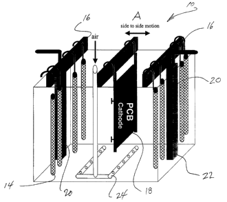
Referring now to Figure 1, shown is a schematic
illustration of the plating bath according to one
embodiment, with the cell being globally referenced by
numeral 10. The cell includes a reaction vessel 12 within
which an electrochemical solution is known to be included,
the solution not being shown. The cell includes a
plurality of anodes 14 which are suitably connected to a
bus bar 16 with the bus being connected to suitable source
of power (not shown). The cathode, shown in the example as
the substrate 18 is disposed in the cell 10 as indicated in
Figure 1. In this example, the substrate comprises a PCB
having a blind vias openings (not shown) and other small
features.
:20
In the embodiment of Figure 1, the ultrasonic
transducers 20 (dashed lines) are positioned within hollow
containers 22 which, in the example, comprise polygonal
titanium containers. Since the plating bath comprises a
conventional DC copper bath, the titanium container was
selected in view of the chemical inertness in this system.
Other variations for the material of which the container is
made will depend on the nature of the solution and the
7
CA 02317233 2000-09-O1
overall cell. To augment deposition, an apertured air hose
24 is connected to a source of pressurized gas (not shown)
such as air, nitrogen, noble gases etc. The gas is bubbled
in the solution to cause localized agitation of the
solution at the cathode 18. Further, the cathode 18 may be
moved relative to vessel 12 laterally in the direction of
arrow A to further assist in deposition. This may be moved
manually or mechanically.
:l0 The titanium containers include a plurality of
ultrasonic transducers 20 as indicated with the total power
for a single container comprising 500 watts at between 20
kHz and 60 kHz and preferably 40 kHz operating frequency.
The two cans employed were inserted between and behind two
pairs of anodes 14 as illustrated in Figure 1 in 600 L of
copper plating bath. The cathode consisted of a blind vias
drilled test panel of a printed circuit board.
with reference to Figure 2, shown is a schematic
20 cross-sectional illustration blind via feature. The
feature is denoted by numeral 26 and includes a metal clad
layer 28, a dielectric layer 30, a second metal clad layer
32 positioned beneath layer 30 and a plated metal layer
broadly denoted by 34. With respect to the symbology used
in Figure 2, the following is representative of the
physical meaning and value/units of the symbols used in
Figure 2:
8
CA 02317233 2000-09-O1
Symbol Physical Meaning Value
and/or
Units
AR Blind via aspect ratio - -
d Blind via diameter um
h Blind via depth ~tm
lb Copper blind via bottom thickness ~.lm
lmin Minimum copper blind vias um
thickness
ltl and Surface copper thickness um
1t2
lWl and Copper blind via wall thickness ~.zm
lWz
P1 Mean microthrowing power parameter
P2 Mean deposit quality parameter
In order to calculate the points for the graphical
illustrations to be discussed hereinafter, the following
formula were used:
[1] AR- h
d
:?0 [2] p _ 2 l,'~+IW+lb x100
' 3 1; + IZ
[3]
31,~ x 100
Iw + lw + Ib
9
CA 02317233 2000-09-O1
Regarding Figures 3 through 8, Table 1 represents the
experimental conditions used to generate the data points.
TABLE 1
Experiment Air Ultrasonic Current
Agitation Agitation Density
(W.cni z) (A.dm-z)
A Yes No 2.2
B No 0.093 2.2
C No 0.19 2.2
D Yes 0.093 2.2
E Yes 0.19 2.2
F Yes No 1.65
G Yes 0.045 1.65
H Yes 0.093 1.65
I Yes 0.19 1.65
J Yes 0.045 2.2
For the data in Figures 3 through 8, a plating time
corresponding to a 25 micron deposit thickness and a side-
to-side motion of the PCB were used. These two conditions
together with air agitation are representative of
conventional conditions used in the PCB plating industry.
All of the lengths (lX) were evaluated using cross-
sectional samples taken at different locations on the PCB.
High P1 values are indicative of uniformity in the deposit
CA 02317233 2000-09-O1
while high PZ are representative of the absence of defects
in the deposits.
The results shown in Figure 3 and 4 demonstrate that
the combination of air and ultrasonic agitation (condition
D and E) were crucial and yielded high P, and Pz relative
to conditions A through C. It was determined that
ultrasonic agitation in the absence of air agitation was
not sufficient.
With respect to Figure 5 through 8, experimentation
involved the combined effect of air and ultrasonic
agitation with the exception of condition F (air agitation
only) .
From an analysis of Figure 3 through 8 significant
improvements in both P1 and P2 values were obtained when
using the combination of air and ultrasonic agitation
relative to those results from condition F. This was found
particularly valid when small apertures with high aspect
ratios were plated. High aspect ratio data is provided in
Figures 5 and 6.
With reference to the combination of Figures 3, 5 and
7, P1 values were noted to approach and in some instances
exceed the 100% level therefore demonstrating the
efficiency of the instant process.
11
CA 02317233 2000-09-O1
Although embodiments of the invention have been
described above, it is not limited thereto and it will be
apparent to those skilled in the art that numerous
modifications form part of the present invention insofar as
they do not depart from the spirit, nature and scope of the
claimed and described invention.
12