Note: Descriptions are shown in the official language in which they were submitted.
CA 02317246 2000-09-O1
Doc. No. CRO-47 CA Patent
IN-PLANE MEMS THERMAL ACTUATOR AND ASSOCIATED
FABRICATION METHODS
FIELD OF THE INVENTION
The present invention relates to microelectromechanical actuators, and more
particular to a thermal actuator having self contained heating capabilities
and providing
in-plane actuation.
BACKGROUND OF THE INVENTION
Microelectromechanical structures (MEMS) and other microengineered devices
are presently being developed for a wide variety of applications in view of
the size, cost
and reliability advantages provided by these devices. Many different varieties
of MEMS
devices have been created, including microgears, micromotors, and other
micromachined
devices that are capable of motion or applying force. These MEMS devices can
be
employed in a variety of applications including hydraulic applications in
which MEMS
pumps or valves are utilized and optical applications that include MEMS light
valves and
shutters.
MEMS devices have relied upon various techniques to provide the force
necessary to cause the desired motion within these microstructures. For
example,
cantilevers have been employed to transmit mechanical force in order to rotate
micromachined springs and gears. In addition, some micromotors are driven by
electromagnetic fields, while other micromachined structures are activated by
piezoelectric or electrostatic forces. Recently, MEMS devices that are
actuated by the
controlled thermal expansion of an actuator or other MEMS component have been
developed. For example, U.S. Patent Application Serial Nos. 08/767,192;
08/936,598,
and 08/965,277 are assigned to MCNC, the assignee of the present invention,
and
describe various types of thermally actuated MEMS devices. In addition, MEMS
devices
have been recently developed that include rotational connections to allow
rotation with
less torsional stress and lower applied force than found with torsion bar
connections. For
instance, U.S. Patent Application Serial No. 08/719,711, also assigned to
MCNC,
CA 02317246 2000-09-O1
Doc. No. CRO-47 CA Patent
describes various rotational MEMS connections. The contents of each of these
applications are hereby incorporated by reference herein.
Thermally actuated MEMS devices that rely on thermal expansion of the actuator
have recently been developed to provide for actuation in-plane, i.e.
displacement along a
plane generally parallel to the surface of the microelectronic substrate.
However, these
thermal actuators rely on external heating means to provide the thermal energy
necessary
to cause expansion in the materials comprising the actuator and the resulting
actuation.
These external heaters generally require larger amounts of voltage and higher
operating
temperatures to affect actuation. For examples of such thermally actuated MEMS
devices
see United States Patent No. 5,881,198 entitled "Microactuator for Precisely
Positioning
an Optical Fiber and an Associated Method" issued March 9, 1999, in the name
of
inventor Haake, and United States Patent No. 5,602,955 entitled "Microactuator
for
Precisely Aligning an Optical Fiber and an Associated Fabrication Method"
issued
February 11, 1997, in the name of inventor Haake.
As such, a need exists to provide MEMS thermal actuated devices that are
capable
of generating relatively large displacement, while operating at significantly
lower
temperatures (i.e. lower power consumption) and consuming less area on the
surface of a
microelectronic substrate. These attributes are especially desirable in a MEMS
thermal
actuated device that provides relatively in-plane, linear motion and affords
the benefit of
having a self contained heating mechanism.
SUMMARY OF THE INVENTION
A MEMS thermal actuator device is therefore provided that is capable of
providing linear displacement in a plane generally parallel to the surface of
a substrate.
Additionally, the MEMS thermal actuator of the present invention may provide
for a self
contained heating mechanism that allows for the thermal actuator to be
actuated using
lower power consumption and lower operating temperatures.
The MEMS thermal actuator includes a microelectronic substrate having a first
surface and an anchor structure affixed to the first surface. A composite beam
extends
from the anchor and overlies the first surface of the substrate. The composite
beam is
adapted for thermal actuation, such that it will controllably deflect along a
predetermined
2
CA 02317246 2000-09-O1
Doc. No. CRO-47 CA Patent
path that extends substantially parallel to the first surface of the
microelectronic substrate.
In one embodiment the composite beam comprises two or more layers having
materials
that have correspondingly different thermal coefficients of expansion. As
such, the layers
will respond differently when thermal energy is supplied to the composite. An
electrically conductive path may extend throughout the composite beam to
effectuate
thermal actuation.
In one embodiment of the invention a two layer composite beam comprises a
first
layer of a semiconductor material and a second layer of a metallic material.
The
semiconductor material may be selectively doped during fabrication so as to
create a self
contained heating mechanism within the composite beam. The doped semiconductor
region may afford a path of least resistance for electrical current. The
doping process
may also enhance the fabrication of contacts on the surface of the anchor.
Additionally,
the composite beam, which is characterized by a high aspect ratio in the z
plane direction,
may be constructed so that the first and second layers lie in planes that are
generally
perpendicular to the first surface of the microelectronic substrate. The
vertical layer of
the composite beam provides for deflection of the beam along a predetermined
path that
extends generally parallel to the surface of the microelectronic substrate.
In another embodiment of the invention, a MEMS thermal actuator includes two
or more composite beams. The two or more composite beams may be disposed in an
array or a ganged fashion, such that the multiple composite beams benefit from
overall
force multiplication. In one such embodiment, two composite beams are disposed
on the
surface of a microelectronic substrate such that the ends of the beam farthest
from the
anchor structure face one another. An interconnecting element is operably
connected to
the free ends of the composite beam. The interconnecting element is configured
so as to
impart flexibility when the two composite beams are actuated in unison. The
flexible
nature of the interconnecting element allows for the overall MEMS thermal
actuator
device to impart a greater distance of linear deflection.
In yet another mufti composite beam embodiment, two composite beams are
disposed on the surface of a microelectronic substrate such that the ends of
the beam
farthest from the anchor structure face one another and the beams are
proximate a flexible
beam structure. The flexible beam structure comprises a platform disposed
between two
3
CA 02317246 2000-09-O1
Doc. No. CRO-47 CA Patent
or more anchors affixed to the substrate. One or more flexible beams operably
connect
the platform and the anchors. The platform is adjacent to the free ends of the
composite
beams such that thermal actuation of the composite beam causes the beams to
operably
contact the platform and deflect it in a generally linear fashion. The
flexible beam
structure that houses the platform compensates for variances that may occur in
the
thermal actuation of the composite beams.
The invention is also embodied in a method for fabricating the MEMS thermal
actuators of the present invention. The method comprises affixing a first
microelectronic
substrate to a second microelectronic substrate. After the second substrate
has been
thinned to a predetermined thickness, a first portion of the MEMS thermal
actuator
construct is then defined in the second microelectronic substrate, including
the first layer
of a composite beam and a portion of the anchor structure. A doping process
may be
undertaken to define a path of least resistance in the first layer of the
composite beam. A
second layer is disposed on the first layer, the second layer and first layer
comprising
different materials that respond differently to thermal actuation. The
variance in thermal
coefficients of expansion causing the first and second layers of the composite
beam to
actuate the composite beam along a predetermined path that extends
substantially parallel
to the surface of the microelectronic substrate
BRIEF DESCRIPTION OF THE DRAWINGS
FIG. 1 is a plan view of a self contained, in-plane, MEMS thermal actuator in
accordance with an embodiment of the present invention.
FIG. 1 A is a perspective view of a self contained, in-plane, MEMS thermal
actuator in accordance with an embodiment of the present invention.
FIG. 2 is a cross-sectional view of the self contained, in-plane, MEMS thermal
actuator shown in FIG. l, in accordance with an embodiment of the present
invention.
FIG. 3 is a plan view of a dual self contained, in-plane MEMS thermal actuator
including an interconnecting element used to facilitate greater linear
displacement, in
accordance with another embodiment of the present invention.
4
CA 02317246 2000-09-O1
Doc. No. CRO-47 CA Patent
FIG. 4 is a plan view of a dual self contained, in plane MEMS thermal actuator
including a flexible beam construct used to facilitate greater linear
displacement, in
accordance with another embodiment of the present invention.
FIGS SA - SG illustrate various stages in the fabrication process of the self
contained, in-plane MEMS thermal actuator, in accordance with a method for
making
embodiment of the present invention.
DETAILED DESCRIPTION OF THE INVENTION
The present invention now will be described more fully hereinafter with
reference
to the accompanying drawings, in which preferred embodiments of the invention
are
shown. This invention may, however, be embodied in many different forms and
should
not be construed as limited to the embodiments set forth herein; rather, these
embodiments are provided so that this disclosure will be thorough and
complete, and will
fully convey the scope of the invention to those skilled in the art. Like
numbers refer to
like elements throughout.
The following description details MEMS thermal actuated devices that are
capable of generating in-plane, linear motion and provide for a self contained
heating
mechanism to effectuate thermal expansion of the materials comprising the
actuator. The
resulting MEMS thermal actuated devices are thereby capable of operating at
significantly lower temperature and power while providing relatively large
displacements. In addition, methods for fabricating such devices are provided
herein.
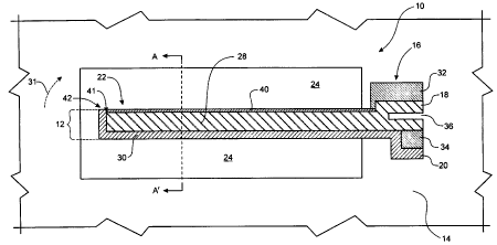
Refernng to FIGS.1, lA and 2, shown, respectively, are a top plan view, a
perspective view and a cross-sectional end view of a self contained, in-plane,
MEMS
thermal actuator 10 in accordance with one embodiment of the present
invention. The
thermal actuator comprises a composite beam 12 that is affixed to the
microelectronic
substrate 14. The composite beam is affixed, at proximal end 16, to the
substrate via an
anchor, shown in FIG.1 as first anchor portion 18 and second anchor portion
20. From
the proximal end, the composite beam extends outward, overlying the
microelectronic
substrate, and concluding in a distal end 22 disposed furthest from the
anchor(s). As
such, the composite beam overlies and is suspended above the microelectronic
substrate
in a cantilever-like configuration. Optionally, the thermal actuator of the
present
5
CA 02317246 2000-09-O1
Doc. No. CRO-47 CA Patent
invention may define a trench 24 disposed in the surface 26 of the
microelectronic
substrate 14 that provides for additional thermal isolation between the
composite beam
and the microelectronic substrate. For example, the cross-sectional view of
FIG. 2
depicts the suspended composite beam disposed above a trench defined in the
microelectronic substrate.
The composite beam will comprise at least two materials that
characteristically
have different thermal coefficients of expansion. As depicted in FIG. 1, the
composite
beam includes a first layer 28 and a second layer 30. It is also possible and
within the
inventive concepts herein disclosed to construct the composite beam with more
than two
layers. As shown in FIG. 2, the first and second layers are disposed
vertically in
relationship to the surface of the microelectronic substrate. The vertical
relationship of
the layers is required to affect actuation in an in-plane direction, parallel
with the
generally planar surface of the microelectronic substrate, as shown by arrow
31. The first
and second layers will, typically, be thin layers of about 1 micron to about
10 microns so
as to facilitate flexibility and movement in the overall composite beam. Since
the layers
have different thermal coefficients of expansion, the layers will respond
differently to
thermal actuation resulting in deflection of the composite beam.
In one embodiment of the invention the first layer 28 may comprise a
semiconductor material, such as silicon, and the second layer 30 may comprise
a metallic
material, such as gold or nickel. In this embodiment the second layer has a
characteristically higher coefficient of thermal expansion than the first
layer. Since the
layer having the higher coefficient of expansion will expand more readily as
temperature
increases, the distal end of the composite beam will bend toward the layer
having the
lower coefficient of thermal expansion when thermal energy is supplied to the
composite
beam. In the embodiment described, in which the second layer 30 has the higher
coefficient of thermal expansion, the layering relationship will effect
movement of the
beam to the right, toward the first layer 28, when reviewed in Fig. 2. It will
be readily
apparent to those having skill in the art, that the layering may be reversed,
so that the
material having the higher coefficient of thermal expansion is on the opposite
side in the
depicted embodiment and, thus, the movement of the beam will be to the left as
viewed in
Fig. 2. Altering various composite beam and thermal actuator characteristics
can vary the
6
CA 02317246 2000-09-O1
Doc. No. CRO-47 CA Patent
amount of deflection observed in the composite beam. Included among these
characteristics are the choice of materials used for the layers, the thickness
of the layers,
and the amount of heat supplied to the composite beam, and structural
discontinuities in
the layers.
The first and second anchor portions 18 and 20 serve to affix the composite
beam
12 to the underlying substrate. The shape of the overall anchor and/or the
anchor
portions is shown by way of example only. The general shape and location of
the anchors
at the proximal end 16 will be dictated by many design factors, including but
not limited
to, the amount of composite beam deflection desired, the coefficients of
thermal
expansion of the composite beam materials, the desired rigidity of the overall
thermal
actuator, etc. First and second contacts 32 and 34 are disposed on respective
first and
second anchor portions 18 and 20. The contacts are interconnected with a
source of
electrical energy (not shown in FIG.1) and serve as connection points for an
electrical
current that runs through the composite beam. The heat generated by the
electrical
current in the beam acts as the means for actuating the composite beam. In the
embodiment shown the two anchor portions are separated by a gap 36. The gap
serves as
an insulator providing electrical insulation between the first and second
contacts.
As mentioned above, the microelectronic substrate 14 may define a trench 24 in
the region underlying the composite beam. Typically, the trench will be
slightly longer
than the length of the composite beam and the maximum deflection distance of
the beam
will dictate the width of the trench. The trench provides heating efficiency
advantages.
For example, the gap created by the trench between the composite beam and the
microelectronic substrate provides thermal isolation and, thus, less heat loss
is
experienced between the composite beam and the substrate. Additionally, the
trench
simplifies the fabrication process used to deposit the metallic second layer
30 upon the
first layer 28. In contrast with conventional horizontal type layering
constructs, the
layers of the composite beam are stacked vertically. To effectuate vertical
layering the
metallic second layer 30 is deposited at an angle to assure uniform coverage
of the
vertical sidewall 38 of the first layer (shown in FIG. 2). Without a trench in
place, there
is a likelihood that depositing the metallic second layer will lead to
electrical shorting of
the underlying microelectronic substrate and any metal elements defined on the
substrate.
7
CA 02317246 2000-09-O1
Doc. No. CRO-47 CA Patent
Alternately, the MEMS thermal actuator of the present invention may be
constructed
without a trench defined in the microelectronic substrate. In such embodiments
a release
layer, typically an oxide layer, is used to release the composite beam from
the surface of
the substrate during fabrication. The releasing process results in a small
gap, typically
less that 1 micron, existing between the microelectronic substrate and the
composite
beam.
The composite beam is adapted for thermal actuation through direct, self
heating
techniques using electric current. As previously discussed prior art in-plane,
thermal
actuators have used indirect heating techniques and have, thus, required large
currents
and high operating temperatures. As such, the high temperature, large current
nature of
prior art thermal actuators makes them less efficient than the thermal
actuator of the
present invention. In order to permit direct heating, each layer of the
composite beam
defines an electrically conductive path that runs in a continuous loop through
the
composite beam and between a first and second contacts 32 and 34 disposed upon
the
anchor portions 18 and 20. In this fashion, an electrical circuit is formed by
passing
current from one contact and through one of the layers of the composite beam
to the
distal end of the composite beam prior to returning to the other contact via
the other
layer. Preferably, the electrically conductive path is disposed so as to
substantially
surround at least one of the layers comprising the composite beam. It is
possible and
within the inventive concepts herein disclosed to alter the configuration of
the electrically
conductive path to form a circuit loop that will effectuate heat in the
composite beam.
The electrically conductive path has a predetermined electrical resistance so
as to permit
thermal actuation of the composite beam when electrical energy is supplied
thereto.
The present invention uses controlled doping to facilitate self heating and to
customize the resistance characteristics of the non-metallic materials used in
the thermal
acuator construct. In this fashion the doped region of the composite beam acts
as the
heater, self contained within the composite beam structure. Materials such as
silicon are
highly resistant and, thus, the doping of such materials aids in constructing
a highly
conductive path for the passage of electrical current. Highly doping silicon
can be
achieved with materials such as phosphorus or boron. The use of doping
techniques is
well known by those of ordinary skill in the art. It should also be noted that
the
8
CA 02317246 2000-09-O1
Doc. No. CRO-47 CA Patent
embodiments herein described are not limited to internal heating to effectuate
actuation.
The MEMS thermal actuators shown here will operate with external heating and
in
certain embodiments, depending on the composition of the substrate and the
materials
used to form the actuator, ambient temperature actuation is possible.
In the embodiment shown in FIGS. 1 and 2, in which the first layer 28
comprises
a semiconductor material, such as silicon, and the second layer 30 comprises a
metal,
such as gold, the external surface 40 of the first layer has been controllably
doped. The
second layer is electrically connected at junction 41 to the doped conductive
surface of
the first layer at the tip 42 of the distal end of the composite beam. The tip
portion of the
distal end may be fabricated so that it is either an extension of the second
layer (as shown
in FIG. 1) or it may comprise a continuation of the doped conductive region of
the first
layer leading into the second layer. Both alternative configurations will
allow for the
second layer to be electrically connected with the doped conductive surface of
the first
layer. Since the doped regions define a path of least electrical resistance,
the electrical
current will mostly follow the path defined by the doped portions of the first
layer and the
metallic second layer, with the undoped portion 28 being an electrical
insulator.
Accordingly, the conductive path is provided between the contacts 32 and 34 by
the
doped portion of the first layer and the metallic second layer. As shown, the
contacts
have also been doped to increase electrical conductivity. It is also possible
to devise
contacts that would not require doping. By way of example, when a source of
electrical
energy is applied between the contacts electrical current would flow from the
first contact
32 along the external surface 40 of the first layer (i.e. the doped region of
the first layer),
through junction 41 into the interconnected second layer 30 and return back
through the
second layer to the second contact 34. In an alternate embodiment the
electrical current
could flow in the opposite direction, emanating from the second contact,
flowing through
the composite beam and completing the path at the first contact.
Referring to FIG. 3, in another embodiment of the present invention the
thermal
actuator includes dual composite beam actuators 102 and 104. A first and
second
composite beam 106 and 108 are disposed proximately such that the distal ends
110 of
the respective beams face each other. The composite beams are adapted to move
in
unison in response to the selective application of thermal actuation. To
assure uniform
9
CA 02317246 2000-09-O1
Doc. No. CRO-47 CA Patent
movement between the composite beams the beams will generally be comprised of
identical layers; similar in material, quantity of layers, layer thickness and
doping
characteristics. The dual composite beams may generally be perceived as mirror
images
of one another.
As shown in FIG. 3, first and second composite beams are adapted to deflect in
the direction of the arrow 112 when thermal energy is applied to the beams.
When a
single composite beam thermal actuator is used initial deflection of the beam
is generally
linear, however as the beam continues to deflect the pattern of deflection
takes on an
arcuate path. In this regard, as thermal energy is applied to the single
composite beam
actuator the beam has a limited range of relatively linear displacement before
the
displacement becomes increasingly more rotary or angular. In the FIG. 3
embodiment
affixing an interconnecting element 114 to the distal ends of each composite
beam
increases linear displacement. The interconnecting element may be formed
during the
fabrication process that defines one of the layers of the composite beam.
Thus, the
interconnecting element may comprise silicon, gold, nickel or a similar
suitable material.
In a silicon embodiment the interconnecting element may be doped or undoped.
If the
interconnecting element is doped, the doping will typically occur simultaneous
with the
doping of the contacts 32 and 34 and the external surface 40 of the first
layer.
Additionally, if the interconnecting element is doped an actuating electrical
conductive
path may exist between the contact 32 of the first thermal actuator 102, the
interconnecting element and the contact 32 of the second thermal actuator 104.
This
electrical configuration would make the second pair of contacts 34 optional.
Alternately,
the electrical path may exist between the second pair of contacts 34 and the
doped
interconnecting element thus, eliminating the need for the first set of
contacts 32.
Preferably, the interconnecting element is shaped and sized so as to impart
flexibility.
The flexible nature of the interconnecting element increases the linear
displacement
distance. In the FIG. 3 illustration, the interconnecting element has a
preferred
wishbone-like configuration. As the composite beams begin to deflect upward,
the legs
116 of the wishbone-like configuration flex outward and result in an overall
linear
displacement of the interconnecting element in the direction of the arrow.
CA 02317246 2000-09-O1
Doc. No. CRO-47 CA Patent
Additionally, the interconnecting element 114 may serve to simplify the
overall
heating arrangement of the dual composite beam thermal actuator. The
interconnecting
element may serve as a bridge that allows the electrical current to flow from
one
composite beam to the next. In the embodiment shown in FIG.3 the
interconnecting
element uses the doped region of the first layer, typically silicon, as the
transfer path
between the first composite beam and the second composite beam. In such a
configuration the electrical bridging capabilities of the interconnecting
element may
eliminate the need to supply electrical current individually to both composite
beams. In
an embodiment in which the interconnect is used as an electrical link it is
more desirable
to have the interconnect element comprise a metal or doped silicon so that
electrical
resistance can be minimized.
Another mufti beam thermal actuator in accordance with yet another embodiment
of the present invention is shown in FIG. 4. This embodiment provides for a
flexible
beam 130 construct disposed proximate the distal ends 110 of the dual
composite beams
106 and 108. In much the same fashion as the dual composite beam thermal
actuator
shown in FIG. 3, the composite beams shown in the FIG. 4 embodiment will
generally
be perceived as mirror images of one another. The dual composite beams are in
operable
contact with a platform 132. The platform is disposed so that it is generally
midway
between the distal end of the first composite beam and the distal end of the
second
composite beam. The platform is operably connected to at least two anchors
that are
affixed to the microelectronic substrate, shown here as first and second
anchors 134 and
136. In the embodiment shown in FIG. 4 the anchors are operably connected to
the
platform via first flexible beam 138 and second flexible beam 140. A series of
springs
142 are located along the beams and serve to provide elasticity to the overall
flexible
beam structure. The fabrication of the platform, the anchors, the flexible
beams and the
springs can be part of the same patterning and etch processes used to form the
first layer
of the thermal actuator construct or they may entail separate processing
steps. As such,
the platform, the anchors, the flexible beams and the springs may comprise
silicon, gold,
nickel or any other suitable material.
In operation the dual thermal actuators are activated by thermal energy and
provide for the generally simultaneous deflection of the distal ends of the
composite
11
CA 02317246 2000-09-O1
Doc. No. CRO-47 CA Patent
beams. Upon actuation the distal ends of the composite beams contact the
platform and
provide the force necessary to move the platform in a linear direction (the
path of the
platform is shown as arrow 144). The beams and the springs allow for the
platform to
move in the linear direction and allow for the platform to relax into a non-
actuated
position upon deactivation of the thermal actuators. This embodiment of a dual
beam
actuator is advantageous because the spring-like beam structure compensates
for any
unequal movement of the respective composite beams and accordingly provides
enhanced linear displacement characteristics as compared to the aforementioned
described single composite beam embodiment.
Numerous other multi beam thermal actuator embodiments are also feasible and
within the inventive concepts herein disclosed. For example, the composite
beams may
be arranged radially, with the distal ends directed toward a control hub to
effectuate
rotational movement. The hub may have levers extending from it that provide
added
actuation force. For a detailed discussion of rotary type MEMS structures see
United
States Patent Application No. 09/275,058 entitled "Microelectromechanical
Rotary
Structures" filed on May 23, 1999, in the name of inventors Hill et al. and
assigned to
MCNC, the assignee of the present invention. That application is herein
incorporated by
reference as if set forth fully herein. Additionally, the composite beams may
be ganged
together and/or configured in an array to benefit from force multiplication,
thereby,
effectively increasing the ability to move objects a greater distance and/or
move larger
objects.
FIGS. 5A - SG illustrate cross-sectional views of various fabrication stages
in
accordance with a method of making the thermal actuator of the present
invention.
Referring to FIG. 5A, a first microelectronic substrate 200 having a first
oxide layer 202
is formed on the substrate and a trench 204 is defined through the first oxide
layer and
into the first microelectronic substrate. The first microelectronic substrate
may comprise
silicon although other suitable substrate material may also be used. The first
oxide layer
is typically disposed on the substrate by a conventional thermal oxidation
process in
which the substrate is exposed to an oxygen environment at elevated
temperature and the
oxide then grows on the substrate. In the embodiment in which the substrate is
silicon,
the first oxide layer may comprise silicon dioxide (Si02). The thickness of
the first oxide
12
CA 02317246 2000-09-O1
Doc. No. CRO-47 CA Patent
layer will typically be about 2000 angstroms to about 8000 angstroms. The
first oxide
layer serves as a dielectric insulating layer and provides a means for
subsequent defining
and etching of the trench. Standard photolithography techniques may be used to
pattern
the region within the first oxide layer that will define the trench. A
conventional wet etch
process may then be used to develop the trench through the first oxide layer
and into the
substrate. The resulting trench typically has a depth within the substrate of
about 10
microns to about 20 microns. The trench will also typically have a length
slightly longer
than the desired predetermined length of the composite beam and a width
consistent with
the maximum deflection of the beam, generally about 100 microns.
FIG. 5B illustrates the first microelectronic substrate having a trench
defined
therein after a second microelectronic substrate 206 has been attached and
polished back.
The second microelectronic substrate will subsequently form the first layer of
the
composite beam and a portion of the beam anchor. In a preferred embodiment the
second substrate will comprise silicon. A standard fusion bonding process is
used to
afl'lx the second microelectronic substrate to the first microelectronic
substrate at the
oxide layer interface. After the second microelectronic substrate is bonded it
is polished
back to the desired predetermined thickness. The thickness of the second
microelectronic
substrate will be consistent with the desired thickness or height of the
resulting composite
beam. Typically, the second microelectronic substrate will be polished back to
a
thickness of about 25 microns to about 50 microns.
Referring to FIG. 5C shown is an oxide structure 208 formed on the second
microelectronic substrate 206. The oxide structures) generally overlie the
area that will
comprise the composite beam and a portion of the anchors. The oxide
structures) result
from a second oxide layer (not shown in FIG. 5C) being disposed on the second
substrate. The similar oxidation process to the one previously used for
disposing the first
oxide layer on the first substrate is typically used to dispose the second
oxide layer. In
the embodiment in which the second microelectronic substrate is silicon, the
second
oxide layer may comprise silicon dioxide (Si02). The thickness of the second
oxide layer
will typically be about 2000 angstroms to about 8000 angstroms. Standard
photolithography techniques may be used to pattern the requisite oxide
structure. A
conventional wet etch process may then be used to develop the oxide
structure(s). The
13
CA 02317246 2000-09-O1
Doc. No. CRO-47 CA Patent
resulting oxide structures) provide dielectric separation, preventing
subsequent doping in
areas underlying the oxide structures) and electrical isolation between
subsequent
conductive regions (i.e., doped regions and metallic regions).
Further processing results in the structure shown in FIG. SD in which a
portion of
the second microelectronic substrate has been etched away to expose one side
of the
thermal actuator. Standard photolithography techniques may be used to pattern
a side of
the overall thermal actuator, including a portion of the anchor structure and
the first
sidewall 210 of the first layer of the composite beam into the second
substrate. A deep
silicon reactive ion dry etch process may then be used to etch away a portion
of the
second substrate and expose a sidewall of the first layer of the composite
beam and a
portion of the anchor structure. A dry etch process is preferred at this stage
to create the
high aspect ratio of the composite beam (about 25-50 microns in depth relative
to an
about 5-7 microns width).
Referring to FIG. SE, shown is the thermal actuator construct after exposed
silicon surfaces have been subjected to a conventional diffusion doping
process. The
doping process provides for a continuous conductive path along the periphery
of the
composite beam and defines the contacts on the anchor. In a typical doping
process
phosphorus may be used as the doping impurity, although other materials may be
used to
create a highly doped region in the second silicon substrate. The doping
process will
create doped regions in all those area not protected by an oxide. As shown in
FIG. SE
the resulting doped regions may include the first sidewall 210 of the first
layer of the
composite beam, the surface of the trench 204, the exposed portion of the
remainder of
the second microelectronic substrate 206 and the regions defining the contacts
on the
anchor (for the sake of not confusing the reader, the anchor structure and,
thus, the
contacts are not shown in the FIG. SA-5G illustrations). The doping of the
surface of the
trench and exposed portion of the remainder of the second microelectronic
substrate is
incidental. The doped region will typically have a depth into the substrate of
about 2000
angstroms to about 8000 angstroms.
FIG. SF depicts the thermal actuator after an additional etch process has
revealed
the definition of the second side of the thermal actuator. After the
completion of this etch
process all that remains of the second substrate are those structures of the
thermal
14
CA 02317246 2000-09-O1
Doc. No. CRO-47 CA Patent
actuator; the first layer and a portion of the anchor structure, that comprise
the material of
the second substrate. FIG. SF illustrates the definition of the second
sidewall 212 of the
first layer after completion of the additional etch process. Standard
photolithography
techniques may be used to pattern into the substrate the remaining side of the
overall
thermal actuator, including a portion of the anchor structure and the second
sidewall of
the first layer of the composite beam. A conventional reactive ion dry etch
process may
then be used to etch away the remainder of the second substrate and expose the
second
sidewall of the first layer of the composite beam and the remainder of the
anchor
structure.
The thermal actuator of the present invention is shown in its completed form
in
FIG. 5G. A second layer 214, typically a metallic layer is disposed on the
second
sidewall 212 of the first layer. The second layer may comprise gold, nickel or
another
suitable material that has a coefficient of thermal expansion that differs
from the
coefficient of thermal expansion of the material chosen to comprise the first
layer. In the
embodiment in which the second layer comprises gold a conventional evaporation
process is used to dispose the layer, typically the layer is about 2 to about
3 microns
thick. In order to properly dispose the second layer on the vertical sidewall
of the first
layer and to assure proper uniform thickness of the second layer the overall
thermal
actuator construct may be placed at an angle during the evaporation process.
The
evaporation process will result in the second layer being disposed on surfaces
not
requiring such. In order to remove unnecessary second layer coverage, a
standard
photolithography process is used to pattern the areas requiring the second
layer and a
conventional wet etch process is used to define the areas requiring second
layer coverage.
In most instances, the etch process will result in second layer coverage
extending above
the second sidewall 212 and partially covering the surface of the second oxide
layer 208.
Additionally, the second layer may remain at the tip of the distal end of the
composite
beam (as shown in FIG. 1 ). Alternately, the tip of the distal end of the
composite beam
may comprise a doped region of the first layer. In the embodiment shown in
FIG. 5G the
first and second oxide layers 202 and 208 remain on the completed thermal
actuator. It is
also possible and within the inventive concepts herein disclosed to remove the
oxide
layer after the second layer has been disposed. The plan and cross-sectional
views of
CA 02317246 2000-09-O1
Doc. No. CRO-47 CA Patent
FIGS.1 and 2 illustrate an embodiment in which the oxide layers have been
removed. In
most instances leaving the oxide layers intact may be desirable as it
eliminates the need
for further processing and may prevent possible electrical shorting.
Accordingly, the fabrication method of this aspect of the present invention
provides an efficient and repeatable technique for creating a vertical layered
MEMS
structure having a doped region that provides for a self contained heating
mechanism.
The resulting MEMS thermal actuated devices are capable of generating large
displacement forces across an in-plane, generally linear direction. These
devices benefit
from the capability of being able to operate at significantly lower
temperature and power
while consuming less surface area on the substrate.
Many modifications and other embodiments of the invention will come to mind to
one skilled in the art to which this invention pertains having the benefit of
the teachings
presented in the foregoing descriptions and the associated drawings.
Therefore, it is to be
understood that the invention is not to be limited to the specific embodiments
disclosed
and that modifications and other embodiments are intended to be included
within the
scope of the appended claims. Although specific terms are employed herein,
they are
used in a generic and descriptive sense only and not for purposes of
limitation.
16