Note: Descriptions are shown in the official language in which they were submitted.
CA 02317368 2000-08-25
O'Brien 4 1
IMPROVED STEPPED ETALON
Technical Field:
This invention is related to an improved mufti-wavelength stepped etalon.
Background 4f The invention:
In many applications, it is necessary to accurately determine the wavelengths)
of
light incident on a suitable detector. A widely used type of detector includes
an etalon to
filter specific frequencies of light. An etalon is a type of interference
filter in which the
intensity of transmitted light is dependent on its wavelength. In a
conventional design,
an etalon is comprised of two partially reflective parallel surfaces a
distance d apart and
separated by a material with an index of refraction r. When collimated light
having a
wavelength ~, is passed through the etalon, some of the light is reflected
from the
surfaces. The multiply reflected light beams interfere, either constructively
or
destructively, with each other, and thus alter the overall intensity of the
light which
passes through the etalon. Maximum transmission occurs when twice the distance
between the reflective surfaces is an integral number of wavelengths ~, in the
etalon. In
other words, 2d*r/a, = x, where x is an integer.
Often, it is desirable to provide a sensor which is sensitive to, and can
discriminate among, several different frequencies of incident light at the
same time. Such
a sensor is particularly useful for spectrographic analysis. Although several
discrete
etalons can be utilized for this purpose, in some implementations, a stepped
etalon is
used instead. In this arrangement, one or both active surfaces of the etalon
are stepped
so that each step on the etalon provides a region of different thickness. By
adjusting the
thicknesses appropriately, each step can be configured to pass different
frequencies of
light. Stepped spectrographic etalon arrangements of this type are shown in
U.S. Patent
No. 4,822,998 to Yokota et al. and U.S. Patent No. 5,144,498 to Vincent.
A newly developed application requires a specifically configured stepped
etalon
to tune the output frequency of a laser. For fiber optic communications in
particular,
CA 02317368 2000-08-25
O'Brien 4 2
accurate tuning of the communication lasers is necessary to permit adjacent
transmission
. channels to be closely spaced, often at wavelengths differing by only 0.4
nanometers or
less. For such closely spaced channels, a laser's wavelength must be tuned to
the
assigned channel with an accuracy of +/- 0.1 nanometers or less. Although only
a single
wavelength of light needs to be detected to tune such a laser, at these high
accuracies,
thermal variations in the thickness of an etalon and slight variations in the
angle of
applied light from normal to the etalon surface can shift the light transfer
function an
unacceptable degree.
According to the new application, the nominal thickness of the etalon can be
chosen so that the periodicity of the etalon filter roughly matches the
periodicity of a
data communication channel spacing, i.e., 1500.12, 1550.52 nm for a system
with a
channel separation of substantially 0.4 nm. Two or more steps are formed on
one side of
the etalon. The step size is selected to be a fraction of the channel
separation, on the
order of 0.1 nm, and is substantially optimized so that a peak or trough in
the
I 5 transmission curve in the region of one step overlaps a steep portion of
the transmission
curve for one or more other steps. In this manner, as thermal changes in the
etalon shift
the transmission curve for one step beyond the desired range, the curve for a
second step
is shifted into the desired frequency. By selecting a particular step
according to a
measured temperature and etalon calibration information, and measuring the
intensity of
laser light transmitted through the selected step of the etalon, a feedback
signal is
provided which can be used to adjust the output wavelength of the laser.
Similarly,
different steps can be selected to compensate for tolerance errors in the
angle of light
incident to the etalon.
With reference to Figs. la and lb, in both views of stepped etalon
configurations,
the stepped etalon 10 has partially reflective coatings I la, l lb and is
positioned adjacent
an appropriately configured array of photodetectors 14a, 14b, where each
detector is
aligned with a corresponding etalon step land 12a, 12b. When a beam of light
16 is
directed onto the etalon 10, the intensity of the output signal attributed to
each detector
14a, 14b indicates the intensity of light passing through the etalon in the
region of the
CA 02317368 2000-08-25
O'Brien 4 3
corresponding step, therefore providing a measure of the intensity of incident
light, with
. the particular frequencies determined by the thickness of the etalon in that
region.
A significant drawback to a conventional stepped etalon is the interference
caused by the abrupt transition between the lands of adjacent steps. When no
step is
present, the intensity within a collimated light beam transmitted through an
etalon has the
same intensity pattern as the incident beam, typically gaussian-like as shown
in Fig. 1 c.
However, when an abrupt step is present, the incident and resonant light is
diffracted by
the step wall 18, producing interference within the transmitted beam along the
z-axis
(perpendicular to the step edge). The resulting fringe pattern is illustrated
in Fig. 1 d.
The result of the diffraction is that in the vicinity of the step, there is
substantial angular
dispersion of the light which reduces the quality of the transmission
fixnction resulting in
reduced signal amplitude, broadened peaks, as well as reduced ability to
differentiate
small changes in the frequency of the input light.
Such a reduction in wavelength discrimination is illustrated in Fig. 1 a for a
two
step etalon. Curves Al-AS are measured on a first step A and curves B 1-BS are
measured on a second step B. Curves A1 and B 1 represent positions distant
from the
step wall. The remaining curves A2-AS and B2-BS are measurements made at
locations
progressively closer to the step wall. The input signal is provided by a
temperature
tuned laser and therefore increases in temperature represent increases in
input signal
wavelength. As indicated, the peaks and troughs for curves close to the step
transition
are lower and less defined than those measured far from the step transition,
indicating
that near the step transition, it is harder to discriminate between
wavelengths that are
close to each other.
The effect of the interference and overall reduction in etalon quality
associated
with abrupt steps creates a "dead spot" behind and near the step edge in which
accurate
intensity readings are compromised. Thus, there are portions of the etalon
where a
detector cannot be placed due to the reduced quality of the transmitted beam.
CA 02317368 2000-08-25
O'Brien 4 4
For example, experiments using an etalon with a thickness of approximately 2mm
and a step height of approximately 0.2 um reveal a "dead spot" approximately
600 to
800 um wide directly behind the step. Since input beam widths of between 0.5
to 5.0
mm are common, a significant portion of the transmitted beam will not have
high quality
etalon transmission characteristics and thus will not be suitable for
detection. This
reduces the available optical power for measurement and lowers the power-per-
detector.
Since a minimum signal-to-noise ratio is required for reliable measurements,
decreasing
the power-per-detector thus can decrease the accuracy of the detector and the
stability of
equipment which is adjusted according to the etalon measurements. The
interference
also limits the number of possible steps which can be placed on an etalon of a
given size.
Although the size of the etalon can be increased to provide more area within
each
step land which is distant from the edge, this is often an undesirable
solution. First, the
detector array is commonly formed on an integrated circuit which may not be as
easily
increased in size without a relatively large increase in production cost.
Second, the
width of the input light beam itself may not be variable and increasing the
etalon width
will introduce the additional problems of directing the beam to the desired
portion of the
etalon.
Summary Of The Invention:
According to the invention, a stepped etalon is formed with a transition
region
between the lands of adjacent steps in the form of a non-planar wall arranged
so that the
points of transition between the adjacent lands vary transversely along a
lateral axis of
the etaton. In particular, the step wall is curved, waved, or otherwise varied
so that the
average height of the stepped surface does not change abruptly in the
transition region
from the height of one land to another, but instead varies gradually according
to the
particular shape of the step wall. In an alternative embodiment, the step
transition is
formed using a grey-scale or half tone patterning in which the average height
gradually
varies across the transition region. While the modified step will still
produce local
interference, the varied shape of the step wall produces varied interference
patterns
which are subject to a lesser degree of constructive combination than is
present with a
CA 02317368 2000-08-25
O'Brien 4 5
flat wall and may advantageously produce destructive combinations which reduce
the net
. interference when measured a distance from the etalon. An etalon according
to the
invention can easily be made using conventional fabrication techniques and
without
additional processing steps.
S Brief Description Of The Drawings
The foregoing and other features of the present invention will be more readily
apparent from the following detailed description and drawings of illustrative
embodiments of the invention in which:
Fig. 1 a is a side view of a conventional stepped etalon;
Fig. 1 b is a perspective view of the etalon of Fig. 1 a;
Fig. 1 c is a graph of the intensity of a light beam transmitted by an
unstepped
etalon;
Fig. 1 d is a graph of the intensity of a light beam transmitted by a stepped
etalon
and passing through the step transition region;
Fig. le is a graph of the intensity of light beams transmitted by a stepped
etalon
measured at different lateral distances from the step;
Fig. 2a is a perspective view of a stepped etalon according to a first
embodiment
of the invention;
Fig. 2b is a top view of the etalon of Fig. 2a;
Figs. 3-5 are top views of the etalon of Fig. 2a having alternative wall
configurations; and
Figs. 6a=6c are top views of a stepped etalon according to a second embodiment
of the invention.
CA 02317368 2000-08-25
O'Brien 4 6
Detailed Description Of The Preferred Embodiment(S):
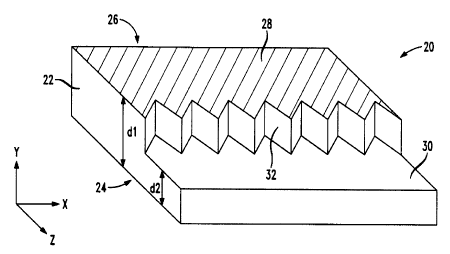
Turning to Figs. 2a and 2b, there is shown a stepped etalon 20 according to
the
invention. The etalon 20 is comprised of a body 22 having a first
substantially flat side
24 and an opposing stepped second side 26. Both sides are covered with a
partially
reflecting surface (not shown) and the body is comprised of a material, such
as Si02,
which is transparent to at least a predetermined range of wavelengths.
The stepped side 26 has a first step land 28 and a second step land 30
separated
by a non-planar wall 32. The lands 28, 30 are substantially flat and parallel
to the first
side 24 and distant from it a respective first and second distance d,, d2. The
wall 32
extends laterally along the x-axis across the etalon 20 and has points of
transition (i.e.,
drop points) that vary transversely along the z-axis within a transition
region 34 to
produce a "wavy" or otherwise curved step wall.
The wavy step wall 32 breaks up the coherent diffraction pattern present in a
conventional straight wall to reduce the net interference caused by the step
as viewed a
1 S distance from the etalon. In other words, as viewed from a distance, the
transition
between the two lands 28, 30 is not as abrupt as a straight wall, but instead
the average
distance from the first side 24 to the second side 26 varies gradually on the
average
across the transition region, where the particular average height depends on
the specific
shape of the step wall 32. In Figs. 2a and 2b, the transition point between
the two lands
28, 30 varies along a triangle or saw-tooth curve. In a particular etalon
embodiment
having a step height dl-d2 of approximately 170 ~ 15 nm, a saw-tooth curve
having an
amplitude of between 100 and 300 um and a period of approximately 100um has
been
found to reduce the net interference caused by the step transition. Of course,
other
scales can be used, as will be apparent to one of skill in the art.
A wide variety of other step wall shapes can be used as well. Fig. 3
illustrates a
smoothly oscillating curve 36, which may lie along a sinusoid or other curve.
In one
embodiment, the curve varies according to the square of the sine of the
lateral position.
For the example etalon having a step height of 170 t 15 nm, a preferred step
wall lies
CA 02317368 2000-08-25
O'Brien 4 7
along a curve z~ A*sin2(~c x/(0.20+0.20x)), where A is the amplitude of the
curve and is
~ preferably between 100 and 300 um.
Fig. 4 is an illustration of a step wall that lies along a square wave 3 8. In
a
preferred configuration for the example etalon, such a square wave has a
period of
approximately 10 um and an amplitude of between about 100 and 300 um.
Alternatively, the curve may also vary in a generally random manner in either
or both of
the period and amplitude, as illustrated in Fig. 5. Other boundaries for the
wall can also
be used to break up the interference patterns, such as various fractal or
fracta.l-like
curves (not shown).
According to a second embodiment of the invention, illustrated in Fig. 6a, the
transition region 34 is comprised of a plurality of elevations 40 which have
surfaces that
are above the second land 30, and preferably are substantially the same height
as the first
land 28 and a plurality of areas 41 having surfaces that are substantially
level with the
second land 30. The elevations 40 can be considered as analogous to pixels
arranged on
a grid 42, shown overlaid on etaton 20 in Fig. 6a for illustrative purposes.
The
elevations 40 are arranged to produce an average height in the transition
region which is
between the first and second distances. Such a configuration can easily be
produced by
selective etching of the surface 26 of the etalon to create the second land 30
and the
areas 41, which etching is controlled by a photoresist deposited in the
transition region in
a manner similar to grey scale or half tone printing techniques.
In a preferred embodiment, the elevations 40 are arranged such that the total
area
covered by the elevation "pixels" 40 decreases transversely (along the z-axis)
across the
transition region from the border 44 with the first land 28 to the border 46
with the
second land 30. The aggregate result is a "fuzzy" transition between the two
lands 28,
30 illustrated in Fig. 6b. It should be noted that the borders 44, 46 of the
transition
region 34 need not be linear, but instead can vary in a manner similar to that
of the wall
in the transition region illustrated in Figs. 2-5. Fig. 6c is an illustration
of a grey-scale
transition having a border 44 which is a random curve. Other variations are
also
CA 02317368 2000-08-25
O'Brien 4 8
possible. While square elevation pixels 40 are illustrated, the pixels can be
of any shape,
which shape can vary among the various elevation pixels 40.
While the invention has been particularly shown and described with reference
to
preferred embodiments thereof, it will be understood by those skilled in the
art that
various changes in form and details may be made therein without departing from
the
spirit and scope of the invention. For example, steps according to the
invention may be
formed on both sides of the etalon.