Note: Descriptions are shown in the official language in which they were submitted.
CA 02317514 2000-07-06
WO 99/35838 PCT/US98/26177
CATV PASSIVE COMPONENT WITH RF
SPLITTER AND POWER ADDING/REMOVAL PORT
BACKGROUND OF THE INVENTION
Field of the Invention
This invention relates generally to cable television
communication system distribution components. More
particularly, the invention relates to a passive signal
component that obviates standard CATV power inserters by
permitting power insertion or extraction in either direction
of a bidirectional cable television communication system.
Description of the Prior Art
Many different types of cable television (CATV)
communication systems exist providing a large diversity of
services. Conventional one-way CATV systems primarily provide
broadcast video services, which are sent over a CATV
transmission network in a downstream direction, from a headend
of a CATV network to a plurality of subscriber terminals.
Bidirectional CATV systems allow subscribers to interact with
their programming providers which have become commonplace in
the industry as the diversity of services has grown. New
services that are under development will rely on the full use
and deployment of the return path communication.
The CATV transmission network usually comprises a trunk
system designed for the bulk transport of the plurality of
CATV services. Bridging amplifiers are used to feed signals
from the trunk system to a distribution syste~t, then onto
individual subscriber drops.
CA 02317514 2000-07-06
WO 99/35838 PCT/US98/26177
-2-
A CATV transmission distribution plant includes coaxial
cables, signal couplers/splitters, amplifiers, and subscriber
taps. When placed in the signal path, passive transmission
devices attenuate the signal. Normally, the system is
designed with unity gain from the headend to each subscriber
terminal, taking into account the signal losses throughout the
trunk, branch lines and subscriber drops. As the signal
proceeds along the distribution system, the attenuation of the
coaxial cable and the burden of passive devices reduces the
signal to a level such that amplification may be required.
Line extender amplifiers, which provide the amplification,
require a source of power.
The line amplifiers are usually suspended by the signal
carrying coaxial cable support strand between telephone poles
and are powered from the signal coaxial cable. Rather than
distributing the power with separate power cables, alternating
current is periodically inserted into the signal carrying
coaxial cable via CATV power inserters.
A power inserter impresses the alternating current source
on the coaxial cable without interfering with the RF signal.
The power inserter houses a low pass filter for 60 cycle, 60
Vac and a band rejection filter for the RF signal present on
the coaxial cable. The power inserter, namely the filter
network, is located in a weather and RFI proof housing and is
also suspended on the cable strand. Pole mounted
ferroresonant transformers provide the reduction and isolation
of the local utility power supply to the power inserter. The
line amplifier separates the RF signal from the impressed 60
CA 02317514 2000-07-06
WO 99/35838 PCT/US98126177
-3-
Vac with a low pass filter to rectify the current for use in
powering the amplifier. A high pass filter passes the RF
signal to the amplifier gain stages.
Rather than using a separate device for power insertion,
it is desirable to include power insertion or extraction at
the signal splitters.
To reduce the complexity of CATV distribution systems and
further increase installation flexibility and overall
performance, it is desirable to include more power insertion
options in standard CATV signal splitters.
SUN~iARY OF THE INVENTION
A CATV signal component is presented that allows direct,
bidirectional power insertion or extraction while providing
RF signal splitting. The signal splitter has a low burden on
the distribution system and can bidirectionally pass
alternating or direct current already impressed on the RF
signal or provide an insertion or extraction function.
Accordingly, it is an object of the present invention to
provide a CATV signal splitter with a power port.
It is a further object of the invention to provide a
signal splitter while allowing either power insertion or
extraction with a minimal system burden.
Other objects and advantages of the signal component will
become apparent to those skilled in the art after reading the
detailed description of the preferred embodiment.
CA 02317514 2003-O1-03
_3a-
In accordance with one aspect of the present invention
there is provided a passive component for splitting RF
frequencies and distributing an impressed current having a
signal input port, a plurality of signal output ports and a
current port comprising: a splitter having an input and a
plurality of outputs; said sputter input coupled to the
signal input port via an upstream power/signal separator
circuit; each of said splitter outputs coupled to one of
the plurality of signal output ports via a downstream
power/signal separator circuit; each of said power/signal
separator circuits having a signal connection, a power
connection and a combined power/signal connection; said
splitter input coupled to said signal connection of said
upstream power/signal separator circuit; each of said
splitter outputs coupled to said signal connection of a
respective downstream power/signal separator circuit; the
signal input port coupled to said combined power/signal
connection of said upstream power/signal separator circuit;
each of said signal output ports coupled to said combined
power/signal connection of said respective downstream
power/signal separator circuit; said power connections of
each of said power/signal separator circuits coupled
together to define a power node; and said power node
coupled to the current port whereby power extraction or
insertion may be performed.
CA 02317514 2000-07-06
a ~ , ~ , , , ,
r v v n t a n ~ i 1 ( n I < n
-4-
BRIEF DESCRIPTION OF THE DRAWINGS
Figure 1 is a block diagram illustrating a typical CATV
forward frequency/return frequency transmission distribution
plant.
Figure 2 is a front view of a CATV enclosure embodying
the present invention.
Figure 3 is a rear view of the removed face plate showing
a typical circuit board layout for the present invention.
Figure 4 is an electrical schematic of the present
invention.
DESCRIPTION OF THE PREFERRED EMBODIMENTS
The preferred embodiment will be described with reference
to the drawing figures where like numerals represent like
elements throughout.
With reference to Figure 1, the topology of a typical
CATV distribution plant 15 for distributing cable television
signals downstream to a subscriber and for receiving return
path messages from a subscriber CATV terminal 17 is shown.
The CATV distribution plant 15 connects a headend to a
plurality of subscribers through subscriber terminals 17. The
distribution plant 15 begins with a coaxial or fiber optic
trunk line 29 coupled to the headend 21. Some portions of the
CATV plant may use optical fiber cable instead of coaxial
transmission cables.
AMEP,~GcD SNEER
CA 02317514 2000-07-06
WO 99/35838 PCT/US98/26177
-5-
medium between headend 21 and subscriber terminals 17 for the
CATV system. Bidirectional signal amplifiers 31 are
distributed throughout the cable plant 15 to boost and
equalize a transmitted signal and insure that proper signal
strength levels are maintained.
A frequency agile RF data return transmitter 33 is
included in each terminal 17 and permits a subscriber to
communicate with the headend 21 by transmitting messages in
the return direction of the CATV plant 15. The headend 21
includes a frequency agile RF data receiver 35 for receiving
messages transmitted by multiple return transmitters 33.
As shown in Figure 2, the present invention 23 includes
an RF signal input port P1, first P2 and second P3 RF signal
output ports and an alternating current input port P4. The
device 23 is housed in a lightweight diecast aluminum alloy
housing 37 with a rotatable faceplate 39 providing strand or
pedestal mounting and RFI shielding. Figure 3 shows the
device 23 with the faceplate 39 removed and the circuit board
visible. The four external ports P1, P2, P3 and P4 couple
internally to a connector platform (not shown). The face
plate plugs into the connector platform coupling the external
ports to corresponding RF input jack J1, first J2 and second
J3 output jacks and an alternating current input jack J4.
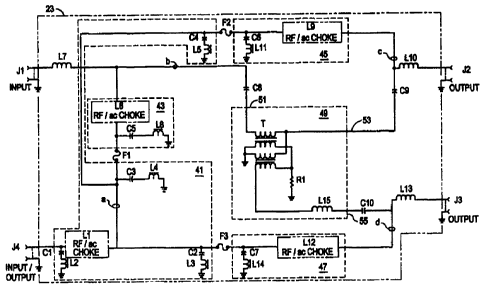
Referring now to Figures 3 and 4, the device 23 includes
both power inserter and signal splitter functions. The power
inserter includes the ac input, filtering and distribution,
and coupling to the RF signal connections.
CA 02317514 2000-07-06
WO 99/35838 PCT/US98/26177
-6-
A three-pole 41 low-pass (low-frequency) filter is
coupled to the signal terminal of the ac input jack J4 and
comprises first Cl, second C2, third C3 and fourth c4
capacitors and a first inductor L1 arranged in a pi-network
with each capacitor having ferrite beads placed on one of
their leads to prevent parasitic oscillations. The ferrite
beads form corresponding second L2, third L3, fourth L4 and
fifth L5 inductors. The pi-network provides low-pass
filtering from an external alternating current power supply
(not shown) which may be local to the device 23.
At a first node a, the filtered alternating current is
distributed by first Fl, second F2 and third F3 fuses to their
respective RF signal jacks J1, J2 and J3. First 43, second
45 and third 47 two-pole, low-pass filters are coupled between
each fuse and RF signal jack to provide additional filtering.
A fifth C5 capacitor and a sixth inductor L5 comprise the
first 43 two-pole low-pass filter. The first 43 filter is
coupled to a seventh L7 inductor at a second node b and to the
first fuse Fl. The seventh L7 inductor is also coupled to the
signal terminal of the RF input jack J1. A ferrite bead
placed on one lead of the fifth capacitor C5 forms an eighth
L8 inductor.
A sixth capacitor C6 and a ninth inductor L9 comprise the
second 45 two-pole low-pass filter. The second 45 filter is
coupled to a tenth L10 inductor at a third node c and to the
second fuse F2. The tenth L10 inductor is also coupled to the
signal terminal of the first RF output jack J2. A ferrite
CA 02317514 2000-07-06
WO 99/35838 PCT/US98/Z6177
bead placed on one lead of the sixth capacitor C6 forms an
eleventh L11 inductor.
A seventh capacitor C7 and a twelfth inductor L12
comprise the third 47 two-pole low-pass filter. The third 47
filter is coupled to a thirteenth L13 inductor at a fourth
node d and to the third fuse F3. The thirteenth L13 inductor
is also coupled to the signal terminal of the second RF output
jack J3. A ferrite bead placed on one lead of the seventh C7
capacitor forms a tenth L14 inductor.
The splitter 49 comprises a fifteenth L15 inductor as a
calculated load, a first resistor R1 and an impedance matching
transformer Tl. The splitter 49 has an input 51 and first 53
and second 55 outputs and are coupled to each RF jack inductor
L7, L10, and L13. The splitter 49 divides the RF signal while
also inserting a calculated loss if required by the cable
network design. The function of a splitter is well known to
those skilled in the art of electronics and a functional
discussion is beyond the scope of the present invention.
Eighth C8, ninth C9 and tenth C10 capacitors form one
pole high-pass filters passing the RF signals to and from the
splitter while blocking the low frequency alternating current.
The eighth C8 capacitor is coupled between the splitter input
51 and second node b, the ninth C9 capacitor is coupled
between the first splitter output 53 and third node c and the
tenth C10 capacitor is coupled between the second splitter
output 55 and the fourth d node.
Since the coaxial cable is a transmission line conveying
high frequency signals, the splitting network permits the
CA 02317514 2000-07-06
WO 99/35838 PCT/US98/26177
_g_
division of the input signal without return reflection. The
individual component values for the preferred embodiment are
shown in Table 1.
TABLE 1
COMPONENT SPECIFICATIONS COMPONENT SPECIFICATIONS
C1 0.047 ~,F, 400 Vac L5 Ferrite Bead
C2 0.01 ~,F, 400 Vac L6 Power Passing Choke
C3 0.01 ~,F, 400 Vac L7 1'/z Turns, '/a in.
Dia.
C4 0.01 ~F, 400 Vac L8 Ferrite Bead
C5 0.047 ~F, 400 Vac L9 Power Passing Choke
C6 0.047 ~,F, 400 Vac L10 1~ Turns, '/s in.
Dia.
C7 0.047 ~,F, 400 Vac L11 Ferrite Bead
C8 910 pF, 500 Vac L12 Power Passing Choke
C9 820 pF, 300 Vac L13 lid Turns, '/s in.
Dia.
C10 910 pF, 500 Vac L14 Ferrite Bead
L1 Power Passing ChokeL15 1'/2 Turns, '/e in.
Dia.
L2 Ferrite Bead R1 82 S2, '/o W
L3 Ferrite Bead T2 Splitter Transformer
L4 Ferrite Bead
The present invention 23 routes the alternating current
through the low-pass filters 41, 43, 45 and 47 between each
jack Jl, J2, J3 and J4. The RF signal is passed between the
RF signal jacks J1, J2 and J3 through the splitter 49. The
high frequency RF signals are blocked by the low-pass filters
establishing a current path while the low frequency
alternating current is blocked by high-pass filters (C8, C9
and C10) establishing a signal path. The RF signal and
alternating current paths are combined at the RF input J1 and
output jacks J2 and J3. Power already present on the cable
27 at either the signal input P1 or output ports P2 and P3 may
CA 02317514 2000-07-06
WO 99/35838 PCTNS98/26177
_g_
be accessed at the alternating current jack ~f4 for powering
other CATV equipment.
The ability to impress an alternating or direct current
source onto a signal is well understood by those skilled in
the art of electronics. The combining of the alternating
current and RF signals at the signal jacks form a composite
waveform with the RF signals carried on the low-frequency
alternating current sine wave. The function of the various
orders of low-pass filters removes the low frequency
alternating current from the composite signal leaving behind
the RF portion which are the CATV services. In the presently
preferred embodiment, alternating current is used to provide
power throughout the CATV infrastructure. It is also possible
that direct current may be similarly impressed upon the signal
creating an offset in the RF signal indicative of the voltage
magnitude.
While the present invention has been described in terms
of the preferred embodiment, other variations which are within
the scope of the invention as outlined in the claims below
will be apparent to those skilled in the art.