Note: Descriptions are shown in the official language in which they were submitted.
CA 02317902 2000-09-07
SIBEPOOIA.CA
1
THREE PORT CONTENT ADDRESSABLE MEMORY DEVICE.AND
METHODS FOR IMPLEMENTING THE SAME
by Inventors
G.F. Randall Gibson
Farhad Shafai
Kenneth J. Schultz
CROSS REFERENCE TO RELATED APPLICATIONS
This application claims priority from U.S. Provisional Patent Application No.
60/153,388 filed on September 10, 1999, and entitled "Content Addressable
Memory
Circuitry" and from U.S. Provisional Patent Application No. 60/167,155 filed
on November
23, 1999, and entitled "Three Port Content Addressable Memory Circuit and
Methods for
Implementing the Same." This application is also related to U.S. Provisional
Application No.
60/166,964 filed on November 23, 1999 and entitled "Content Addressable Memory
Circuit
with Redundant Array and Method for Implementing the Same." These provisional
applications are incorporated herein by reference.
BACKGROUND OF THE INVENTION
1. Field of the Invention
The present invention relates generally to memory devices, and more
particularly to a
content addressable memory device for providing uninterrupted search
operations
synchronized with read/write operations and independent search and maintenance
interfaces.
2. Description of the Related Art
Memory devices are indispensable components of modern computer systems. As
storage devices, they are used to provide fast access to data and instructions
stored therein.
Content addressable memory (CAM) is a special type of memory that is often
used for
performing address searches. For example, Internet routers often include a CAM
for
searching the address of specified data. The use of CAMs allows the routers to
perform
address searches to allow computer systems to communicate data with one
another over
networks. Besides routers, CAMs are also utilized in other areas such as
database searches,
image processing, and voice recognition applications.
CA 02317902 2000-09-07
SIBEPOOlA.CA
2
CAMS generally include a two-dimensional row and column content address memory
array of core cells, such that each row contains an address, pointer, or bit
pattern entry. Based
on such array of cells, a CAM may perform "read ''and "write" operations at
specific
addresses like a conventional random access memory (RAM). In addition, it also
performs
"search" operations that simultaneously compare a bit pattern of data known as
"comparand"
against an entire list (i.e., column) of pre-stored entries (i.e., rows) of
bit patterns in the CAM
array.
Conventional CAMs are typically two port devices. FIG. lA shows a block
diagram
of a conventional two-port CAM 100. The CAM 100 includes an input port 107 and
an
output port 109. The input port 107 communicates data and control signals over
a data bus
102 for communicating data and an instruction bus 104 for transmitting
instructions
associated with an operation to be performed. The data bus 102 is used to
receive a
comparand or write data as inputs and is thus shared for performing either a
search operation
or a write operation.
1 ~ The output port 109 is shared for a search operation or a read operation.
Specifically,
the output port 109 outputs either search results or read results from the
CA1VI 100 via an
output bus 106. In a search operation, for example, the CANI 100 may output a
search result,
via output bus 106, in the form of an address, pointer, or bit pattern
corresponding to an entry
that matches the input data. Alternatively, the read results may be output
through the data bus
102.
The conventional CAM 100 typically performs operations such as search, read,
and/or
write operations in sequence. FIG. 1B shows an exemplary sequence of
operations that are
serially performed in successive memory clock cycles by the CAM 100. As shown
in FIG.
1B, the CAM performs a series of operations beginning with three "search"
operations, a
"write" operation, two "search" operations, a "write" operation, two "read"
operations, and
ending with two "search" operations. These operations are performed one after
another, in
sequence, with each operation being performed in at least one clock cycle.
Unfortunately, however, the sequential nature of the CAM operations degrade
the
performance of a CAM by delaying search operations. This is because the "read"
and "write"
operations interrupt "search" operations. As can be appreciated, the
interruption in such
search operations presents a significant impediment to high speed "real time"
successive
address searching and thereby complicates system design. For example, Internet
routers are
CA 02317902 2000-09-07
S1BEPOOIA.CA
3
often called upon to perform many searches of routing tables stored in their
CAMS. In such
situations, interruptions in searches delay the processing of search
operations and thus slow
down the response times of computer systems in general.
Additionally, the sharing of the input port 107 by comparand and write data
typically
requires multiplexing of comparand and write data for input to the CAM 100
Similarly, the
sharing of the output port 109 for outputting search results and read results
also entails de-
multiplexing these results. FIG. 1C shows a more detailed block diagram of the
conventional
two-port CAM 100 with a multiplexes 111 and a de-multiplexes 113. The CAM 100
includes
a control block 108 and a CAM array 110. The multiplexes 111 receives a
comparand and/or
write data as inputs and selects either the comparand or the write data for
output in response
to a control signal. The selected output from the multiplexes 111 is then
provided to the data
bus 102 for input to the CAM array 110.
To control the operation of the CAM 100, control signals are provided to the
instruction bus 104 for input to the control block 108. In response to the
control signals, the
control block 108 generates another set of control signals for controlling the
operations of the
CAM array 110. In a search operation, the CAM array 110 outputs, on the result
bus 106 an
address, pointer, or bit pattern (collectively referred herein as "address")
corresponding to an
entry or word in the CAM array 110 that matches the input data on the data bus
102. For a
read operation, on the other hand, the CAM outputs on the result bus 106 data
corresponding
to the address provided on data bus 102.
The demultiplexer 113 is coupled to receive an output result from the output
bus 106
as an input. When the CAM operation is a search operation, the demultiplexer
113 routes the
output result onto a search data bus 115. On the other hand, when the CAM
operation is a
read operation, the demultiplexer 113 routes the output result onto a read
data bus 117.
FIG. 1D shows another block diagram of the conventional CAM 100 in more
detail.
The CAM 100 includes data bus 102, instruction bus 104, result bus 106,
control block 108,
CAM array 110, multiplexes (MUX) 112, comparand register 114, global mask
registers 116,
status register 118, and address counter 120. The control block 108 receives
instructions for a
desired operation through instruction bus 104, and generates the control
signals for the
"search," "read," and "write" operations of the CAM array 110. The CAM 100
illustrated in
FIG. 1D is commercially available, for example, as model NL85721 Ternary
Content
Addressable Memory IPCAM from Netlogic Micosystems, Inc.
CA 02317902 2000-09-07
S1BEPOOIA.CA
4
Unfortunately, using a multiplexing scheme in performing read/write and search
operations adds complexity in implementing conventional two-port CAMS with
attendant
increase in cost. Furthermore, the multiplexing scheme slows down overall CANI
performance since read/write data cannot be input or output simultaneously in
a same clock
cycle with a search data or result. Indeed, a read or write operation must
"steal" cycles from
the search operations because the buses 102 and 106 are shared.
In view of the foregoing, there is a need for a CAM device and method that can
perform read/write operations and search operations simultaneously without
multiplexing
input data and output results so as to improve CAM performance.
SUMMARY OF THE INVENTION
The present invention fills this need by providing three-port content
addressable
memory (CAM) devices and methods for implementing the same. It should be
appreciated
that the present invention can be implemented in numerous ways, including as a
process, an
apparatus, a system, a device, or a method. Several embodiments of the present
invention are
described below.
In one embodiment, the present invention provides a three-port CAM device
including
a CAM, a search control block, and a maintenance control block. The CAM is
configured to
store data. The search control block is arranged to receive search data and
search control
signals via a first port for searching the search data in the CAM. The search
control block is
further configured to perform search operations by accessing the CAM. The
search
operations are performed within search cycles with each search operation being
performed
over multiple clock cycles. In this configuration, more than one search
operations are capable
of being performed simultaneously over one or more clock cycles. Search
results of the
search operations are output via a second port. The maintenance control block
is configured
to perform read/write operations by reading or writing specified data in the
CAM via a third
port.
In another embodiment, the present invention provides a method for performing
search operations and read/write operations in a CAM device. In this method, a
CAM is
provided for storing data. Search data and search control signals are then
provided to a search
control block via a first port for searching the search data in the CAM. The
search control
block is configured to perform search operations by accessing the content
addressable
CA 02317902 2000-09-07
SIBEPOOIA.CA
memory. The search operations are performed within search cycles over multiple
clock
cycles. More than one search operations are capable of being performed
simultaneously over
one or more clock cycles. Search results from the CAM are output via a second
port.
Read/write operations are performed by reading or writing specified data in
the CAM via a
5 third port.
In yet another embodiment, a three-port CAM device for accessing a CAM
containing
data is disclosed. The three-port CAM device includes a content addressable
memory for
storing data, a first port, a second port, and a third port. The first port is
configured to receive
search data and search control signals for searching the search data in the
content addressable
memory. Search operations are performed by accessing the content addressable
memory.
The second port is configured to output search results from the content
addressable memory.
The third port is configured to communicate read/write data to and from the
content
addressable memory for read/write operations.
Advantageously, the three-port arrangement of the present invention
effectively
1 S separates search datapath and read/write datapath. This allows read/write
operations to be
performed during search clock cycles without corrupting or otherwise
compromising the
search results. Furthermore, allowing a read/write operation to be performed
in a search cycle
speeds up search operations by eliminating search interruptions caused by
read/write
operations. Accordingly, the devices and method of the present invention
provide a faster
speed of operation at a given clock frequency. Other advantages of the
invention will become
apparent from the following detailed description, taken in conjunction with
the accompanying
drawings, illustrating by way of example the principles of the invention.
BRIEF DESCRIPTION OF THE DRAWINGS
The present invention will be readily understood by the following detailed
description
in conjunction with the accompanying drawings, wherein like reference numerals
designate
like structural elements.
FIG. lA shows a block diagram of a conventional two-port content addressable
memory (CAM).
FIG. 1B shows a sequence of operations that can be sequentially performed in
successive memory clock cycles by the CAM shown in FIG. lA.
CA 02317902 2000-09-07
SIBEPOOlA.CA
6
FIG. 1 C shows a more detailed block diagram of the conventional two-port CAM
with
a multiplexer 111 and a demultiplexer 113.
FIG. 1D shows another block diagram of a conventional CAM in more detail.
FIG. 2A shows an exemplary three-port CAM device 200 that separates search
datapath and read/write datapath in accordance with one embodiment of the
present invention.
FIG. 2B illustrates a timing diagram showing a sequence of operations
performed by
the three-port CAM device in accordance with one embodiment of the present
invention.
FIG. 2C shows a more detailed block diagram of the three-port CANI device in
accordance with one embodiment of the invention.
FIG. 3A shows a more detailed block diagram of a maintenance control block
according to one embodiment of the invention.
FIG. 3B shows a more detailed block diagram of a search control block
communicating with a CAM array in accordance with one embodiment of the
present
invention.
DETAILED DESCRIPTION OF THE PREFERRED EMBODIMENTS
An invention for a three-port content addressable memory (CA1VI) device that
allows
uninterrupted search operations while performing read and/or write operations
is disclosed. In
the following description, numerous specific details are set forth in order to
provide a
thorough understanding of the present invention. It will be understood,
however, to one
skilled in the art, that the present invention may be practiced without some
or all of these
specific details. In other instances, well known process operations have not
been described in
detail in order not to unnecessarily obscure the present invention.
FIG. 2A shows an exemplary three-port CAM device 200 that separates search
datapath and read/write datapath in accordance with one embodiment of the
present invention.
The three-port CAM device 200 includes three ports: a search input port 262, a
search result
port 266, and a maintenance port 264. The search input port 262 communicates
input search
data, search control signals, and search clock signals over search bus 202,
search control bus
20~, and search clock bus 208, respectively. The search result port 266
communicates search
results over a search result bus 206. Separated from the search input and
search result ports
262 and 266, the maintenance port 264 is arranged to communicate read/write
data, read/write
CA 02317902 2000-09-07
SIBEPOOlA.CA
7
control signals, and read/write clock signals over read/write data bus 203,
re~d/write control
bus 207, and read/write clock bus 209, respectively.
The three-port CAM device 200 is configured to perform search operation and
read/write operations. Specifically, for a search operation, the CAM device
200 is provided,
via search input port 262, with search data over the search bus 202, search
control signals
over the search control bus 205, and a search clock over a search clock bus
208. The search
result is then provided through the search result port 266 via the search
result bus 206 as an
output. On the other hand, for a read and/or write operation, the CAM 200
receives
read/write control signals, via maintenance port 264, over a read/write
control bus 207,
read/write data over a read/write data bus 203, and a read/write clock over a
read/write clock
bus 209. It should be noted that the clock signals provided over the search
clock bus 208 and
read/write clock bus 209 may be the same clock signal.
The three-port CAM device 200 with separate search and read/write datapaths
allows
read/write operations to be performed in the same clock cycle as a search
operation. For
example, FIG. 2B illustrates a timing diagram 250 showing a sequence of
operations
performed by the CAM device 200 in accordance with one embodiment of the
present
invention. In this timing diagram, search operations are performed in sequence
for clock
cycles 252, 254, 256, and 258 with one search operation being performed for
each clock
cycle. Initially, only a search operation takes place in cycle 252. Then in
the next cycle 254,
both a search operation and a write operation are performed. During this
cycle, the CAM
device 200 performs the search operation via search port 262 and performs the
write operation
within the same clock cycle 254 via maintenance port 264.
During the next cycle 256, a search operation and a read operation are
performed. In
this cycle 256, the CAM device 200 performs the search operation and performs
the read
operation within the same clock cycle 256. Then, in the next clock cycle 258,
the CAl'vI
device 200 performs another search operation. In this manner, read/write
operations are
performed in the same cycle as search operations without compromising or
corrupting search
results. It should be noted that the search operations may persist over
multiple clock cycles.
In addition, multiple searches may be underway simultaneously over the clock
cycles.
In addition, by allowing a read/write operation to be performed within the
same clock
cycle as a search operation, the read/write operations no longer interrupt or
interfere with
search operations. Accordingly, the three-port CAM device 200 of the present
invention may
CA 02317902 2000-09-07
SIBEPOOIA.CA
8
perform search operations without the delays caused by sharing read/write and
search
datapaths in conventional two-port CAM devices. This also simplifies the
system level
design by separating the search datapath from the maintenance (e.g.,
read/write) datapath.
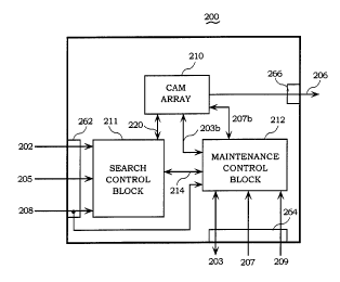
FIG. 2C shows a more detailed block diagram of the three-port CAM device 200
in
accordance with one embodiment of the invention. The three-port CAM device 200
includes
a CAM array 210, a search control block 211, and a maintenance control block
212. The
search control block 211 receives, via search input port 262, search data over
the search data
bus 202, search control signal over the search control bus 205, and search
clock over the
search clock bus 208. The maintenance control block 212 receives, via
maintenance port 264,
read/write control signals over the read/write control signal bus 207,
read/write data via
read/write data bus 203, and read/write clock signal over the read/write clock
bus 209. The
CAM array 210 is coupled to the search and maintenance control blocks 211 and
212 to
communicate data and control signals over buses 220, 203b, and 207b. It should
be noted that
the term "block" as used herein refers to a device, apparatus, subsystem, and
the like, and may
be used interchangeably with such terms.
In this three-port configuration, the search control block 211 generates and
communicates control signals along with specified search data over the bus 220
to search for
the search data in the CAM array 210. Upon completion of the search, the CAM
array 210
outputs the address of the specified data over the search result bus 206 via
search result port
266. The maintenance control block 212, on the other hand, controls read/write
operations.
Specifically, the maintenance control block 212 generates and communicates
control signals
along with specified data over buses 203b and 207b to read or write the data
in the CAM
array 210. For example, the maintenance control block 212 receives the data
(e.g., data and
address for writing, address for reading) and control signals over the data
bus 203 and the
control bus 207. It then transmits the data and control signals over the data
bus 203b and the
control bus 207b for reading or writing the data in the CAM array 210. In a
read operation,
the CAM array 210 provides the data over bus 203b to the maintenance control
block 212,
which outputs the data over the data bus 203. To synchronize the search
operation with
read/write operations, the search and maintenance control blocks 211 and 212
communicate
synchronization signals over a synchronization bus 214.
Alternative embodiments of the invention may include CAiMs with multiple CAM
arrays, multiple search control blocks, multiple maintenance control blocks,
or separate read
CA 02317902 2000-09-07
SIBEPOOIA.CA
9
control blocks and write control blocks. In addition, multiple copies of data
rxlay be stored in
multiple banks. For example, in a two-bank arrangement, the data may be read
or written
from one bank while searches take place in the other bank. Alternative
embodiments of the
invention may also include a CAM with one or more CAM arrays incorporating
internal
search or maintenance control blocks or a CAM in a non-array format.
Furthermore,
alternative embodiments of the invention may include a CAM with additional
control signals,
either static or dynamically clocked devices, multiple clock signals, or
separate substrates.
Maintenance operations other than read or write such as chip configuration or
register
operations may also be handled by the maintenance port.
FIG. 3A shows a more detailed block diagram of the maintenance control block
212
according to one embodiment of the invention. The maintenance control block
212 includes a
clock bridge 216 for arbitrating clocks and a pair of finite state machines
213 and 218. The
finite state machine 213 receives read/write control signals over read/write
control bus 207
and read/write data over read/write data bus 203. The finite state machine 213
also receives a
read/write clock over the read/write clock bus 209. Additionally, the finite
state machine 213
generates control signals by parsing received control signals and captures the
read/write data.
It then transmits the generated control signals over control bus 215 to the
clock bridge 216,
which synchronizes the search and read/write clocks received on the search
clock bus 208 and
read/write clock bus 209. Further, the finite state machine 213 may be used to
control the
handshaking between a processor port (not shown) and an external chip port
(not shown).
In response to control signals received over the control bus 215, the clock
bridge 216
generates and communicates control signals via control signal bus 217 to the
other finite state
machine 218. The finite state machine 218 receives search clock from the
search clock bus
208 and synchronizes the read/write operations with search operations via
control bus 214. It
also generates and communicates read/write control signals via read/write
control bus 207b
and 203b to the CAM array 210 for performing read/write operations. A bus 203a
is provided
between the finite state machines 213 and 218 to allow communication of data
in read/write
operations. For example, in a write operation, data flows from finite state
machine 213 to
finite state machine 218 via bus 203a. Conversely for a read operation, data
flows from finite
state machine 218 to finite state machine 213 via bus 203a. The finite state
machines 213 and
218 may be as simple as one or two logic gates.
CA 02317902 2000-09-07
SIBEPOOIA.CA
FIG. 3B shows a more detailed block diagram of the search control block 211
communicating with the CAM array 210 in accordance with one embodiment of the
present
invention. The search control block 211 includes a search finite state machine
230 and a
capture and pipeline search data device 234. The capture and pipeline search
data device 234
5 receives as inputs search data over the search data bus 202, search control
signal over the
search control bus 205, a search clock over the search clock bus 208. Upon
receiving such
signals, the capture and pipeline search data device 234 generates and
communicates control
and data signals to the CAM array 210 over a control and data bus 235.
The search finite state machine 230 receives the search clock over the search
clock bus
10 208, and generates and communicates control signals over control bus 232 to
CAlvI array ? 10.
In addition, it generates and communicates synchronization control signals
over control bus
214 to the finite state machine 218 of the maintenance control block 212. In
one
embodiment, the search finite state machine 230 may be implemented by using
the finite state
machine 218. The control bus 232 and the control and data bus 235 correspond
to the control
and data bus 220 shown in FIG. 2C. The CANI array 210 also communicates
control signals
over control bus 207b and 203b with the maintenance control block 212.
A cascade control block 237 is provided to receive the search clock over
search clock
bus 208 and output data (e.g., search address) over data bus 236 from the CAM
array 210. It
then provides the output data to the search result port 266 via search result
bus 206. In
addition, the cascade control block 237 is configured so that a set of CAM
chips 200 may be
connected in parallel to allow for concatenating a plurality of content
addressable memories to
hold a larger number of entries of specified data. The cascade control block
237 may be an
output buffer when the three-port CAM device 200 is used alone. In one
embodiment, the
cascade control block 237 may be included in the search control block 211.
Alternatively, it
may be provided as a separate output stage in the CAM device 200.
Thus, the present invention enhances search operations of the CAM array while
allowing read and write operations to be performed during the search cycles.
Whereas the
conventional CAMS have typically performed search and read/write operations
sequentially in
separate clock cycles, allowing a read/write operation to be performed in a
search cycle
speeds up search operations by eliminating interruptions. Accordingly, the CAM
devices of
the present invention provide a higher throughput at a given clock frequency.
CA 02317902 2000-09-07
SIBEPOOlA.CA
11
It should be understood that the various block diagrams may be embodied in any
form
which may include, for example, any suitable semiconductor substrate, printed
device board,
packaged integrated device, or software implementation. Accordingly, those
skilled in the art
will recognize that the present embodiments are to be considered as
illustrative and not
restrictive, and the invention is not to be limited to the details given
herein, but may be
modified within the scope and equivalents of the appended claims.
GYhat is claimed is: