Note: Descriptions are shown in the official language in which they were submitted.
CA 02318050 2000-07-12
.. ..
~ ~ " .. ~~ ~~ . , . .
.. ~. ~ ~ ~ ' ' ' . . .
~ ~ , . .. ~ ~ ~ , . , .
Wo99136331 ~ ~ ,~ ~ i ~~~~ ~~~ ~,
~'Cf jt1S99/01011
.... ..
11ME1<i~E~ SHEET ~ EPO - Munic~t
26
I PEAIEP
2 8. Jan. 2000
MICROWAVE FOOD SCORCH SHIELDING
Backsround of the Envention
This invention relates to the field of packaging materials for
foodstuffs, specifically to the field of packaging foodstuffs for microwave
irradiation. In the past, such packaging contained the foodstuff and may have
included a susceptor for concentrating thermal energy for heating or cooking
the
food contained in the package. Such packages typically did not protect the
foodstuff from overhearing or overcooking, other than in certain embodiments,
to reduce or eliminate the concentration caused by the susceptor or in the
folds
of such packaging. One typical example is microwave popping of popcorn,
which is conventionally done in a paper bag carrying a susceptor. Once the
popcorn is popped it has been found that it is easily scorched by continued
exposure to microwave irradiation. 'The prior art has heretofore not addressed
such continued exposure of the foodstuff to overlong microwave irradiation.
The presen~ ention overcomes thy~ deficient of the prior art by
a
providing an~~~hich~is initially substantially transparent to microwave
irradiation (allowing normal microwave heating and cooking). Upon reaching a
predetermined temperature, the structure of the present invention morphs, or
changes its own form, to a microwave shielding structure, preventing further
heating or cooking (or scorching) of the foodstuff.
~~n .ug_A_ c~ 22g 334 . a Slob in' cL ~c~ o~'''~~l vu, ~ rW c~WrvU~ t~ntr~''
~~ .
-~ ~~ ~ ~~.Ltivr~. ~:._S(pt-b~~~'~ u'' ih a posi~'a~ a~
.t Ld ~- ~' c~ ~ .t h r~ lr~,~ c~ a ~-c ~ c r l~.v~. hid ~ ~o p ~!
~ . . . . '~.~d ~~~1'~'i. It ('~ . .
.P_ d d0~1 31'I
'~ n _ (.. /~ , ~ ~,ri, ~h ~ a.(' c,r~.~r~ ~rt'~
?YfrUI~a_ rn i uv w~,tJlG t~G~~ri'~~%f ~~.~ ~"~ '~' -, rc~,c~.oG ~ ~ e~rna'
rcti H Sid h r-t,~oi., r~ ~,t ~'!~ shnnk~ iv.,~b~'~i~
n,icrvw~wv~C, '~ ASSi l'~ .S~o~' ~ ~"~GrL~ ~'~.C. ~~ ca~~ /~' ~~'~~~
CA 02318050 2000-07-12
WO 99!36331 2 PCT/US99/01011
Brief Description of the Drawings
Figure 1 is a perspective view of a microwave popcorn bag useful
in the practice of the present invention.
Figure 2 is a detailed plan view of a structure useful in the
practice of the present invention before being irradiated by microwave energy.
Figure 3 is a detailed plan view of the structure of Figure 2 after
undergoing a transition in response to irradiation by microwave energy.
Figure 4 is a side section view of a portion of the bag of Figure 1
showing the structure of Figure 2, taken along lines 4-4 in Figures 1 and 2.
Figure 5 is a side section view similar to that of Figure 4, except
showing the structure of Figure 3.
Figure 6 is a composite view of various embodiments useful in
the practice of the present invention in schematic simplified form both before
and after microwave irradiation.
Figure 7 is a perspective view of a paper layer having printed
conductive material thereon, similar to Figures 2 and 4.
Figure 8 is an alternative embodiment to that shown in Figure 7,
with powder coating material replacing the printed conductive material.
Figure 9 is a further alternative embodiment to that shown in
Figures 7 and 8 with conductive material particles suspended in an insulating
solvent.
Figure 10 is a composite view of a solder dot embodiment of the
present invention showing side and top section views of a microcircuit before
and after microwave irradiation.
Figure 11 is a simplified side view illustrating particle spreading.
Figure 12 is a simplified perspective view illustrating particles
coalescing.
Figure 13 is a top plan view of the effect of particle spreading and
coalescence.
CA 02318050 2000-07-12
-WO 99/36331 3 PCT/US99/01011
Figure 14 is a is a simplified side view of a composite powder
coating showing a composite material made up of metal and flux before and
after microwave irradiation.
Figure 1 S is a perspective view of the embodiment of Figure 9
before and after microwave irradiation.
Figure 16 is a perspective view of the embodiment of Figure 9
illustrating certain aspects of the present invention.
Detailed Description of the Invention
Referring to the Figures, and most particularly to Figure 1, a
microwave-compatible food package in the form of a popcorn bag 10 which is
useful in the practice of the present invention may be seen. Bag 10 is
preferably
a layered construction, having an inner layer 12, an outer layer 14 and a
central
layer 16. Inner and outer layers 12, 14 are each preferably formed of
microwave
transparent material such as paper or plastic. Central layer 16 is an
interrupted
pattern or dispersion of microwave reflective material, such as metal. One
such
pattern or arrangement may be seen in plan view in Figure 2, and in more
detail
in side section view in Figure 4. In addition to (and separate from) the
structure
for the present invention, bag or package 10 may have a conventional susceptor
18 attached thereto. It is to be understood that the structure of the central
layer
16 may be utilized as other than a central layer while still remaining within
the
spirit and scope of the present invention; for example, the pattern of
microwave
reflective material described with respect to the central layer 16 may be
positioned "off center" in a laminated construction, or may be utilized as an
outer layer, if desired.
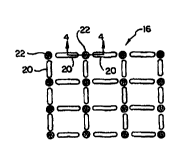
As shown in Figures 2 and 4, in this embodiment the interrupted
pattern of central layer 16 is preferably formed of spaced apart metallic
elements
20, 22. Elements 20 may be printed conductive material such a plurality of
spaced apart metal segments, which may be formed as dashes. Elements 22 are
CA 02318050 2000-07-12
WO 99/36331 q. PCT/US99101011
similarly spaced apart conductive segments, which may be formed as dots
spaced between but not contacting the dashes 20. It is to be understood that
the
dashes are preferably of a material not affected by microwave irradiation, nor
by
the temperatures reached in the practice of the present invention, while the
dots
22 are designed to be affected by such microwave irradiation, or more
particularly, by the thermal effects of such irradiation on the foodstuff or
package (or both).
The present invention provides a structure that is transparent to
microwave irradiation during an initial period of exposure and then becomes
reflective to the microwave energy after the predetermined exposure, thus
shielding the contents of the bag or package from scorching or overheating
upon
the continued application of microwave energy.
In the embodiment shown in Figures 1-5, the dots 22 will melt
upon the application of the predetermined microwave exposure raising the
temperature to a predetermined melting point, upon which occurrence the
elements 22 will contact the elements 20, forming an uninterrupted pattern to
provide microwave shielding thereafter. Figures 3 and 5 show the post-
irradiation (shielding) pattern. In practice, once the temperature of the
central
layer 16 exceeds a predetermined value, the dots 22 will undergo a phase
change
and electrically short out to adjacent elements 20, resulting in an
uninterrupted
pattern 26, as shown in Figures 3 and S. As will become apparent with respect
to other embodiments, the pattern can be regular or irregular or random,
provided that initially it will permit passage of microwave energy (preferably
without substantial impediment), and further provided that in its final,
shielding
state, it is substantially impermeable (preferably reflective) with respect to
impinging microwave irradiation.
When the central layer becomes reflective,
s = sZma,«1
with the equivalent condition:
CA 02318050 2000-07-12
WO 99/36331 g PCT/US99/01011
Qh»3 x 1 OZ°SZ 1 (2)
where 8 is a microwave interaction parameter, 8 is the penetration depth of
the
electromagnetic field in the metallic central layer 26, h is the thickness of
the
metallic central layer 26, ~, is the wavelength of the electromagnetic energy
field,
and a is the conductivity of the metallic central layer 26.
In order to confirm that the pre-irradiation dimensions of the
central layer 16 do not result in microwave screening,
b»4nwha/c (3 )
where b is the gap between adjacent metallic elements 20, 22, w is the radian
frequency of the microwave field, h is the thickness and a is the width of the
microwave elements 20, 22, and c is the speed of light (3x101°cm/s). It
has been
found that if b»1 ~,m, the central layer (in its initial state) will not
provide any
substantial microwave screening at 2450 MHz. It is also to be understood that
the length of each of the elements 20, 22 is to be much less than a quarter
wavelength of the microwave frequency of interest. Here, with the microwave
frequency at 2450 MHz, the wavelength is 12.25 cm.
The reflection and absorption coefficients (the ratios, respectively,
of the reflected and absorbed energy to the incident energy) of an array of
metallic particles of radius R each deposited on a plane surface with density
n
{per unit area) are:
Ofref = nR2{R/~,)4K (4)
(where K = 0.026 for R«S, and K = 0.002 for R»$), and
oc~ _ (nR238)/2~, for R»8 (Sa)
oc~ _ [(nRz38)/2~,](2~R8/~.2) for R«8 (Sb)
For R = 0.1 mm, 8 = 0. O 1 mm, and riR2 = 0.01, aref ~ 10-14 and
ota~ ~ 104. (It is to be understood that the symbol ~ as used herein means "on
the order of or "in the range of'.) :Furthermore, a sheet made up of such
particles so as to have a thickness h = nR3 will have:
CA 02318050 2000-07-12
'WO 99/36331 ( PCT/US99/01011
oc,~ _ { 1-9/n for h«b, 1-8/4~~, for h»8 } (6)
oca~ _ { 9/n for h«S, 8/4n~, for h»8 } . (7)
If oc~r is set to ~ 0.999999 and oc~ is set to ~ 0.00001 (the conditions of a
relatively goad reflector and bad susceptor) the restriction on particle
radius is
found to be R>1 micron. (It is to be understood that the symbol ~ as used
herein
means "about".)
To prevent inter-particle arcing, it is assumed that the particles are
ellipsoidal, each characterized by a long dimension a, and a short
(transverse)
dimension b. The linear dimension of the space between adjacent particles is
d.
The field between isolated and closely adjacent conductive ellipsoids is:
E ; Eo(a/b)2(1+b/d) (8)
and when notice is taken that the dielectric strength for many materials is
approximately Ea~ = 107 to 108 V/m, and the electric field strength in
conventional microwave ovens is of the order Eo = 1 KV/m, the condition of
non-arcing is:
max{(a/b), (a/d)} < (Ea~lEo)~~ = 100. (9)
In order to have the metallic particles follow the package
temperature, it has been found desirable to make the particle radius R be much
less than lmm to avoid any significant time lag due to the thermal mass and
consequent thermal inertia of the particle with respect to the overall package
temperature. Of course, it may, in certain circumstances be found desirable to
delay the transition to the shielding state, and in such occasions, the
particle size
may be increased to provide for such a delay.
Referring now to Figure 6, it is contemplated to be within the
scope of the present invention to have a structure which morphs or changes its
form from a microwave transparent (dielectric) phase to a microwave reflective
{shielding) phase, illustrated by the method of connectingisolated segments to
CA 02318050 2000-07-12
WO 99/36331 ~ PCT/US99/01011
undergo the change as shown from form 16 to form 26, or to achieve the desired
shielding result by melting discrete particles 30 to achieve a connected
pattern
32, or to precipitate conductive particles from an isolated suspended state 34
to a
conducting, precipitated state 36.
Various embodiments of the central layer 16 may be seen in
Figures 7, 8 and 9. In Figure 7, a printed microcircuit 38 having non-
microwave
reactive particles 40 and solder dots 42 is secured to a paper substrate or
layer
44. In Figure 8, conducting particles 46 (made, for example, of metal) are
applied to a substrate 44 by powder coating. In Figure 9, metal or other
conducting particles 46 are held in suspension by an insulating solvent 48,
such
as a resin or volatile material capable of being driven off by heat. It is to
be
understood that, as shown, the particles in Figures 8 and 9 are considerably
magnified from the scale of the particles 40 in Figure 7.
Referring now to Figure 10, a non wetting embodiment of the
microcircuit 38 may be seen. In this Figure, side section views 50, 52 are
taken
along lines B-B and D-D, respectively, and top section views 54, 56 are taken
along lines A-A and C-C, respectively. It is to be understood that views 50
and
54 are before microwave irradiation, and views 52 and 56 are as the
microcircuit
appears after microwave irradiation. This embodiment utilizes a "lobed" solder
form 58 located between a protective layer 60 (such as plastic) and a
substrate
62 (such as paper). Microcircuit elements 64 are spaced apart from solder
element 58 before irradiation, as can be seen in views 50 and 54. At this
time,
elements 64 and 58 do not significantly block microwaves from penetrating the
composite packaging made up of protective layer 60, microcircuit elements 58
and 64, and substrate 62. As the embodiment shown in views 50 and 54 is
heated, the solder will change shape to that shown in Figures 52 and 56,
effectively forming a microwave-shielding microcircuit because of the
"relaxation" of the solder element to the shape 66. The characteristic
reshaping
time is determined by the viscous flow in response to surface tension once the
CA 02318050 2000-07-12
w0 99/36331 g PCT/US99/01011
solder material liquifies. The reshaping time, ~tr, can be estimated as:
i~ = rlR2/yh (10)
where rl is the viscosity, and y is the surface tension. (It is to be
understood that
the symbol = as used herein means "approximately equal to" with, for example,
a scale factor omitted.) For R = 0.lcm and h = 0.01 cm, ~f can be as short as
one
second. Care must also be taken to avoid perforation or penetration of the
protective layer and the paper substrate due to the solder tendency to assume
a
spherical shape. Assuming the contact angle ~ is small (typical for unwetting
surfaces) the estimate
p = (4ycos~)/h ( 11 )
gives p = 104 to 105 dyne%m2 which is considerably less than a typical
ultimate
paper strength of about 10'° dyne/cm2.
In the microcircuit embodiment, it is to be understood that the
melting of solder dots 42 must occur before the food has an opportunity to
burn
or scorch. Furthermore, even unwetting metallic elements 40 can be utilized
with dots or other shapes formed of solder, such as are illustrated in Figure
10.
In connection with using powder coating to form the switchable
microwave shielding layer, the processes of powder particle spreading and
coalescence are to be considered. Referring to Figure 11, particle spreading
is
illustrated graphically with a single particle of an initial radius 68 Ro and
a final
spread length 70 R, where the spreading time, i~, can be estimated by:
is = (vR/~y)(R/Ro)3 = (10 310 5)(R/Ro)3 sec (12)
where Dy is the wetting energy (of the same order of magnitude as the surface
energy). The coalescence time, i~, can similarly be estimated as:
i~ = rIR2/hy = ( 10 3~ 1 O-5)(R/h) sec ( 13 )
where R is the initial radius 72 and h is the thickness 74.
Thus it may be seen that each of the spreading time and coalescence time can
be
considerably smaller than 1 second. A macroscopic top plan view of the
phenomena of spreading and coalescence is shown in Figure 13, where a layer
CA 02318050 2000-07-12
'WO 99136331 9 PCTIUS99/01011
of paper 76 is initially coated with discrete metal particles 78 using a
conventional powder coating process. Spreading of the particles 78 is
illustrated
at 80, with eventual coalescence into a relatively continuous metal sheet 82
(which may have some apertures 84 remaining). As is well known, the
apertures will not adversely affect shielding, provided that the dimensions of
each aperture are much less than a wavelength of the applied microwave field.
In addition to powder coating using all metal particles, it is to be
understood to be within the scope of the present invention to use a composite
powder coating technology such as illustrated in Figure 14, with metal
particles
86 embedded in organic flux 88 (such as epoxy resin) to form composite
particles 89 having a desired melting temperature to achieve a shielding
structure 90 formed of contacting metal particles on substrate 92. In this
embodiment, the metal particles 86 may remain intact or may, alternatively,
melt
to form a relatively continuous sheet 82 such as shown in Figure 13. In the
practice of powder coating the layer to serve as a microwave shield, tin based
powders may be used with particle radii about 10 mm and with a melting
temperature in the range of 40 to 31 ~5 C. Alternatively, sintering metal
powders
may be used to form a conducting (shielding) layer.
Referring now to Figures 15 and 16, still another approach is to
use metal particles 94 dispersed and suspended in a solvent-containing coating
96. Coating 96 is to be understood to be physically stable at conventional
storage and room temperatures and is capable of being volatilized at a desired
predetermined elevated temperature. The initial volume fraction of metal
particles to the total volume is preferably less than about 10 percent. As the
solvent is purposely evaporated, the volume fraction of metal particles rises,
and
a microwave shielding structure 98 is formed on substrate 100 as the metal
particles 94 come into contact with each other. The characteristic solvent
evaporation time, ie, depends on both the solvent material parameters and the
paper porosity:
CA 02318050 2000-07-12
WO 99/3b331 1 p PCT/US99101011
ie = lo/[na3va(1+lPna )] (14)
where n is the concentration of saturated vapor, v is the molecular velocity,
a is
the molecular radius, a is the paper porosity, to is the solvent layer
thickness
102, and lp is the covering paper (protective layer) thickness 104.
The invention is not to be taken as limited to all of the details
thereof as modifications and variations thereof may be made without departing
from the spirit or scope of the invention.