Note: Descriptions are shown in the official language in which they were submitted.
CA 02318189 2000-07-20
WO 99/38323 PCTIUS98/Z6178
CATV PO~R IN88RT3R
HACRGROtI»TD OF TEE INVENTION
Fiold of the Invention
This invention relates generally to cable television
communication system distribution components. More
particularly, the invention relates to a power inserter having
dual power supply ports that can be internally configured to
source power directionally or to use independent mains power
supplies for dedicated directions in a CATV distribution
system.
Description of the Prior Art
Cable television (CATV) services are provided to
customers through a transmission network that typically
includes a trunk system transporting the plurality of CATV
services from a cable headend to smaller branches and then
onto individual subscriber drops. The transmission medium for
the branch and subscriber drops is usually coaxial cable. To
provide for the transmission of the CATV services, the
transmission network includes cable taps, cable splitters,
line amplifiers and other miscellaneous equipment to
distribute the CATV services.
A typical CATV cable plant is designed with unity gain
from the headend to each subscriber terminal. Signal losses
and gains throughout the trunk, branch lines and subscriber
drops are noted and adjusted to maintain unity gain
throughout. However, many of the aforementioned devices that
distribute the cable services burden the system. As the CATV
CA 02318189 2000-07-20
WO 99/38323 PCTIUS98IZ6178
-2-
signal proceeds throughout the distribution system, the
attenuation of the coaxial cable and the insertion loss of
passive devices reduce the signal to less than unity thereby
requiring periodic amplification. Line amplifiers are
installed and adjusted accordingly to maintain unity gain.
Line amplifiers are usually suspended by the signal
carrying coaxial cable support strand and are powered from the
signal carrying coax cable. The usual method of distributing
the mains power supply to each line amplifier is by impressing
or inserting the alternating current on the coaxial cable via
a CATV power inserter.
A power inserter consists of a low-pass filter designed
for 60 cycle, 60 Vac and a band rejection filter for the RF
signal components present on the coaxial cable. The power
inserter is housed in a weather and RFI proof enclosure and
is also suspended on the cable strand. At a line amplifier,
filters separate the CATV RF signal from the impressed 60 Vac.
The RF signal is amplified with the ac component providing the
power source.
Power is usually supplied to a power inserter by a
ferroresonant transformer located on a nearby telephone pole.
The primary side of the ferroresonant transformer is connected
to a single phase power supply from the local utility.
Ferroresonant transformers provide isolation, regulation, and
if necessary, reduction from the mains power supply.
The power inserter can provide power for several line
amplifiers. Shown in Figure 1 is a simplified branch 15 of
a CATV distribution system. A prior art power inserter 17 is
CA 02318189 2000-07-20
-3-
shown sourcing four line amplifiers 19 on either side of the
power inserter 17. A ferroresonant transformer 21 is shown
sourcing the power inserter 17. Both power and signal flow
are bidirectional within the coaxial cable 23.
A schematic for the prior art power inserter 17 is shown
in Figure 2. The power inserter 17 has a single power jack
or port 25, and first 27 and second 29 RF jacks or ports. The
alternating or direct current 31 is filtered using a first 2-
pole (2nd order) low-pass filter comprised of a first inductor
33 coupled to first 35 and second 37 parallel capacitors. The
current flow for both coaxial cable directions is limited with
first 39 and second 41 fuses to their respective first 27 and
second 29 RF jacks. Power insertion may be directional in
dependence upon one or both fuses being installed. The output
from the first fuse [38] 39 is low-pass filtered through a
second 2-pole low-pass filter 47 and coupled to the signal
conductor of the first RF jack 27. The output from the second
fuse 41 is low-pass filtered through a third 2-pole low-pass
filter 49 and coupled to the signal conductor of the second
RF jack 29. To allow the RF signal to pass freely between the
first [43] 27 and second [45] 29 RF jacks, a sixth capacitor
51 forms a high-pass filter between the RF terminals blocking
the low frequency current thereby giving direction to power
flow.
s J ~:4
d~~.~;e~m6~i~~ ro.i:~ .fr~6F -,
CA 02318189 2000-07-20
-4-
A variation of the single source power inserter 19 is
shown in Figures 3 and 4. A dual alternating or direct
current source power inserter 53 is shown having two isolated
ac terminals (depending upon the configuration of an internal
jumper 54) each sourcing a dedicated RF terminal. However,
the prior art dual source power inserter 53 has limitations
when configuring the power inserter 53 concerning isolation
between RF terminals and power ports.
In order to increase the number of sourcing options
available in one cable television power inserter, it is
desirable to have a low cost device that can provide common
or isolated directional power insertion or distribution.
SU1~IARY OF THE INVENTION
A CATV power inserter is presented that allows for a
plurality of power sourcing options while providing superior
isolation between the RF signal and the power supply insertion
points. The power inserter achieves the variety of
configurations by using a four point terminal block having
uniform, compatible dimensions allowing simple connecting
bars, fusing and current limiting options to be quickly
interchanged thereby increasing economy.
Accordingly, it is an object of the present invention to
provide a CATV power inserter having dual power supply ports .
It is a further object of the invention to provide a
power inserter allowing multiple configurations for single or
'~' ~ ' ~ ~'"' '-'.' ,~s
a:7wyiS~~I : G P.~~'....,.
... .....' S,~t~~. .-rp
CA 02318189 2000-07-20
_5_
dual power supplies and the capability of easily adding
current limiting functions.
Other objects and advantages of the power inserter will
become apparent to those skilled in the art after reading the
detailed description of the preferred embodiment.
BRIEF DESCRIPTION OF THE DRAWINGS
Figure 1 is a block diagram of a prior art CATV
distribution branch with a single ac/dc port power inserter
and line amplifiers.
Figure 2 is a prior art schematic of the single ac/dc
port power inserter.
Figure 3 is a block diagram of a prior art CATV
distribution branch with a dual ac/dc port power inserter and
line amplifiers.
Figure 4 is a prior art schematic of the dual ac/dc port
power inserter.
Figure 5 is a CATV power inserter embodying the present
invention.
Figure 6 is an alternative configuration of the present
invention having a common high current ac/dc port.
Figure 7 is an alternative configuration of the present
invention having a single, directional ac/dc port.
Figure 8 is an alternative configuration of the present
invention having a single, directional ac/dc port.
CA 02318189 2000-07-20
-6-
Figure 9 is an alternative configuration of the present
invention having dual isolated directional ac/dc ports.
Figure 10 is an alternative configuration of the present
invention having dual isolated, directional ac/dc ports with
current limiting.
Figure 11 is an alternative configuration of the present
invention having dual isolated, directional ac/dc ports with
active surge suppression circuitry.
DESCRIPTION OF THE PREFERRED EMBODIMENTS
The preferred embodiment will be described with reference
to the drawing figures where like numerals represent like
elements throughout.
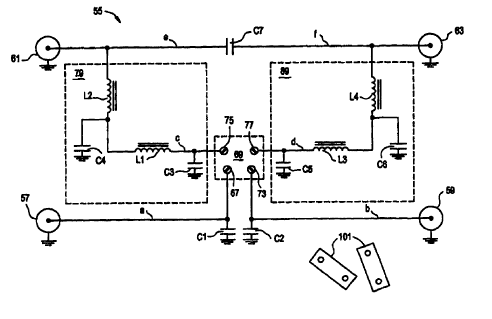
With reference to Figure 5, a power inserter 55 embodying
the present invention is shown. The power inserter 55
includes four external connections; first 57 and second 59
ac/dc jacks or ports and first 61 and second 63 RF signal
jacks or ports. The individual components of the power
inserter 55 are assembled on a printed circuit board (PCB?
which is housed in a lightweight diecast aluminum alloy
housing with a rotatable face plate providing strand or
pedestal mounting and RFI shielding. The power inserter 55
includes dual ac/dc ports, distribution, and coupling to the
RF signal jacks.
The first ac/dc jack 57 is shunted with a first capacitor
Cl forming node a. Node a is also coupled to a first terminal
'~, ,1,>b ~21~a!'~,o
CA 02318189 2000-07-20
_7_
67 of a configurable terminal block 69. The second ac/dc jack
59 is shunted with a second capacitor C2 forming node b. Node
b is coupled to a second terminal 73 of the configurable
terminal block 69. The configurable terminal block 69
includes third 75 and fourth 77 terminals forming nodes c and
d respectively.
Node c is coupled to a first 79 4-pole low-pass filter
including third C3 and fourth C4 capacitors and first L1 and
second L2 inductors . The second inductor L2 is coupled to the
signal carrying conductor of the first 61 RF jack forming node
e.
Node d is coupled to a second 89 4-pole low-pass filter
including fifth C5 and sixth C6 capacitors and third L3 and
fourth L4 inductors . The fourth inductor L4 is coupled to the
signal carrying conductor of the second 63 RF jack forming
node f.
Coupled between the signal carrying conductors of the
first 61 and second 63 RF jacks (Nodes a and f) is a seventh
C7 capacitor for passing high frequencies.
The individual component values for the preferred
embodiment are shown in Table 1.
TABLE 1
COMPON~1T SPBCIFICATIONS COMPONENT SPECIFICATION
C1 .O1 ~F, 1000 Vac L1 Power passing choke
2 5 C2 .O1 ~F, 1000 Vac L2 Power passing choke
.,~ ~ ~.
af~lyy~~;1~_yj~,~ v 9i~ s'....
~h..
CA 02318189 2000-07-20
_8_
C3 .O1 ~F, 1000 Vac L3 Power passing choke
C4 .047 ~.F, 1000 L4 Power passing choke
Vac
C5 .O1 ~CF, 1000
Vac
C6 .047 ~CF, 1000
Vac
C7 500 pF, 1000 vac
A discussion of passive filters using inductors and capacitors
of various orders (poles) is beyond the scope of this
specification and is well understood by those skilled in the
art of electronics. Referencing the schematic shown in
Figure 5 one can see that by coupling individual connecting
bars 101 between the terminals 67, 73, 75, and 77 of the
configurable terminal block 69, various power supply
combinations dictating direction can be easily achieved by the
present invention. Power can be directed through the various
nodes (nodes a-f) to either signal jack 61, 63. As one
skilled in this art realizes, the present invention can also
act as a power source or tap since the current flow is
bidirectional.
Referencing Figures 6, 7 and 8, configurations of the
configurable terminal block 69 that allows either the first
57 or second 59 ac/dc jacks to apply power to the power
inserter 55 in dedicated directions at the physical location
where the power inserter 55 is placed on the coaxial cable 23
are shown. Figures 7 and 8 show configurations where power
insertion is directional as to the configuration of the
terminal block 69 and whether power is applied to the first
~~~'~a..~ ~da~..~,.as' ~i~r.
CA 02318189 2000-07-20
_g_
57 or second 59 ac/dc jacks. The ac/dc jack not coupled is
open-circuited. Figure 7 shows the connecting bar 101 placed
to allow current to flow from the first ac/dc jack 57 to the
first RF jack or port 61. Figure 8 shows the connecting bar
101 placed to al low current to f low from the second ac/dc j ack
59 to the second RF jack or port 63.
The configuration shown in Figure 9 allows independent
mains power to be applied in separate, dedicated cable
directions at the location of the power inserter 55. In this
configuration, two connecting bars 101 are used isolating both
the first 57 and second 59 ac/dc jacks from each other and
allowing separate directional power insertion paths with
different current requirements through to their respective RF
j acks .
Figures 10 and 11 show optional circuit boards 107, 109
that have four terminals aligned to couple with the
configurable terminal block 69. Figure 10 shows a simple
fusing arrangement that includes first F1 and second F2 fuses
that provide protection to the mains power supply wiring for
the first 57 and second 59 ac/dc jacks. The first fuse F1
couples the first 67 and fourth [75] 77 terminals of the
configurable terminal block 69 (not shown). The second fuse
F2 couples the second 73 and third [77] ~ terminals of the
configurable terminal block 69 (not shown). As can be
appreciated by one skilled in this art, the fuse values may
. ~, ~~ P ~ ~; ~ ~-a ""'~ ~" r..F ~"~'~
~a.~~yx?6;~"a. ~
CA 02318189 2000-07-20
-10-
vary in consideration of the upstream mains sourcing
capability and wire ampacity. The present invention 55 can
be configured for varying numbers of line amplifiers located
on either side of the power insertion point. A similar
function is shown in Figure 11 with dual active surge
suppression. The first current limiting circuit llla couples
the first 67 and fourth [75] 77 terminals of the configurable
terminal block 69 (not shown). The second current limiting
circuit lllb couples the second 73 and third [77] 75 terminals
of the configurable terminal block 69 (not shown). In this
configuration, active current monitoring is employed for each
path of power insertion. This configuration limits the range
of the current draw to a predetermined value.
While the present invention has described in terms of the
preferred embodiment, other variations which are within the
scope of the invention as outlined in the claims below will
be apparent to those skilled in the art.
~d~~#~~~;~~~'~~~~