Note: Descriptions are shown in the official language in which they were submitted.
' CA 02318597 2000-09-12
Korisch 7-14-1-38 1
ANTENNA PACKAGE FOR A MIIRELESS COMMUNICATIONS
DEVICE
Background Of The Invention
This invention relates to wireless communications
devices and, more particularly, to an improved small, low
cost antenna package for such a device.
The greater capacity and larger number of providers for
Personal Communications Services (PCS) means far greater
competition for wireless subsc:ribers. Although total revenue
is soaring, revenue per subscriber has been declining as many
casual and emergency-only users enter the market. In
response, equipment provider: are under pressure to keep
terminal costs low, and at the same time support an
increasing number of features that will increase revenue per
subscriber. Wireless data transmission is one of the growth
areas for wireless services, with increasing demand for
wireless images, financial information and Internet access.
Although a conventional cellular phone can be used as a
wireless modem to transmit data, transmission rates are low
and bit error rates are high. Subscriber acceptance of data
via this mode has been relatively weak. Although the higher
frequency and bandwidth of PC~~ provides some improvement, it
does not offer the significant increase in bit rate that
makes data transmission attractive to a wide customer base.
Antenna diversity doers provide this significant
improvement. Spatial diversity with a switching algorithm
can increase the system gain by 3-5dB depending on the
effectiveness of the algorithm and the isolation between
antennas. As an example, a simple switch algorithm monitors
only the one antenna signal in use. When this signal falls
below some threshold value, it switches to the other antenna.
A more complicated algorithm would monitor both antenna
signals and switch to the one with the strongest signal even
CA 02318597 2000-09-12
Korisch 7-14-1-38 2
if they are both above the opE:rational threshold. Even more
complicated systems would rep~.icate much of the RF train and
monitor both signals closer to digital baseband. The higher
average gain attained with switched diversity allows lower
bit error rates to be achieved at higher data rates.
Realizing enough separation between the antennas is an
important consideration in spatial diversity on a handset .
Horizontal separation is snore effective than vertical
separation because the decorrelation of the received signal
increases faster with horizontal separation, particularly
when the vertical beamwidth is smaller than the horizontal
beamwidth as it is when one of the antennas is an omni-
directional dipole. The signals have to be essentially
uncorrelated and the first nu:Ll in correlation factor occurs
when the distance between antennas is approximately 0.38
times the wavelength. Practically, a correlation coefficient
below 0.25, and in some cases below 0.50, can be neglected,
providing effective separations of as little as 1/5 the
wavelength. This is about 8 cm at 900 MHz and 4 cm at 1.9
GHz. The problem with diver~;ity in a small terminal with a
size less than one half t:he wavelength is that it is
difficult to determine the center of the radiation since the
entire housing radiates through near field coupling,
especially when the antenna is inside. So although the
distances required for effective diversity can be realized on
the handset, the actual situation is much more complicated.
When the antennas are different types and positioned
differently, then other type: of diversity (directional and
polarization) may have an effect as well.
It is therefore apparent: that a need exists for small,
low cost antennas for use as diversity antennas in handheld
wireless communications devices.
CA 02318597 2002-10-04
3
Summary Of T'h~ Invention
According to the present invention, there is provided
an antenna package for use in a wireless communications
device. The inventive package includes a metallic
leadframe section having a plurality of leads and a paddle
shaped as an antenna. Dielectric material encapsulates
the paddle and portions of the leads.
In accordance with an aspect of this invention, the
paddle is shaped as a planar inverted F antenna (PIFA).
In accordance with another aspect of this invention,
the package further includes electronic circuitry attached
to the leadframe section and encapsulated. by the
dielectric material.
Fabrication of the aforedescribed package includes
the step of providing a metallic leadframe section having
a plurality of leads and a paddle shaped as an antenna.
The leadframe section is positioned along the parting line
of a mold, and in registration with a mold cavity. The
mold cavity is filled with molten dielectric material so
as to encapsulate the paddle and portions of the leads.
The dielectric material is allowed to harden. The
.encapsulated leadframe section is removed from the mold,
and the unencapsulated portions of the plurality of leads
are then trimmed.
In accordance with a preferred aspect of this
invention there is provided a method for fabricating an
antenna package for use in a wireless communications
CA 02318597 2002-10-04
3a
device, comprising the steps of: providing a metallic
leadframe section having a plurality of leads and a paddle
shaped as an antenna; providing a mold having a parting
line and at least one cavity; positioning the leadframe
section along the mold parting line and in registration
with a mold cavity: filling the mold cavity with molten
dielectric material so as to encapsulate the paddle and
portions of the leads allowing the dielectric material to
hardens removing the encapsulated leadframe section from
the moldy and trimming the unencapsulated portions of the
plurality of leads.
Brief Description Of The Drawings
The foregoing will be more readily apparent upon
reading the following description in conjunction with the
drawings in which like elements in different figures
thereof are identified by the same reference numeral and
wherein:
FIGURE 1 is a cross sectional view of an illustrative
planar antenna
CA 02318597 2000-09-12
Korisch 7-14-1-38
FIGURE 2 is a cross secaional view showing a first
embodiment of an antenna pack<~ge constructed in accordance
with this invention and mounted with respect to a circuit
board, the package being contoured to the outer case of a
wireless communications device;
FIGURE 3 illustrates two types of interconnection to a
printed circuit board for an antenna package according to
the present invention;
FIGURE 4 is a side across sectional view of a
capacitively coupled planar inverted F antenna constructed
with a leadframe in accordancE~ with the principles of this
invention;
FIGURE 5 is a "transparE~nt" top view of the antenna
shown in Figure 4;
FIGURES 6-9 illustrate an integrated antenna and radio
components package with a formed EMI/RFI shield, with Figures
6 and 7 being top and side views, respectively, before the
shield has been formed and with Figures 8 and 9 being top and
side views, respectively, aftE:r the shield has been formed;
FIGURES 10A, 10B, 11, 12~s, 12B, 13A and 13B illustrate
steps in the formation of an antenna package according to the
present invention;
FIGURE 14 illustrates t:he separation of individual
antenna packages from a group of leadframes which have been
molded together; and
FIGURE 15 illustrates th.e forming of the leads of an
individual package.
Detailed pescription
Upon consideration of the problem of providing diversity
antennas in a handheld wireles;~ communications device, it was
CA 02318597 2000-09-12
Korisch 7-14-1-38
initially decided to use the dipole (whip) as one antenna and
utilize as a second antenna one which is small enough to be
integrated within the housing of the handheld device. A
particularly suitable small antenna is a planar inverted F
antenna (PIFA). One such antenna for dual band operation is
disclosed in U.S. Patent No. 5,926,139, issued to Korisch on
July 20, 1999. Figure 1 is a cross sectional view of such an
antenna where a ground plane 22 is on a first side of a
dielectric substrate 24 and a radiating element 26 is on the
other side of the dielectric substrate 24. A feed pin 28
extends through the ground plane 22 and the substrate 24 to
couple the radiating element 26 to transceiver circuitry (not
shown) and is insulated from. the ground plane 22 by an
insulating via 30.
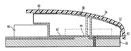
To fit the planar antenna within the housing of the
device, polyurethane or other suitable material may be used
to form a casting of the unused. volume of the interior of the
device between the printed circuit board and the housing. As
shown in Figure 2, this casting is utilized to produce a
plastic piece 32 which conforms to a portion of the interior
space of the device between the: outer case 34 and the printed
circuit board 36. Alternative:Ly, other known techniques can
be utilized to produce a plastic piece conforming to the
desired shape. A radiating patch 38 having the desired
antenna configuration is then mounted to the plastic piece 32
on a surface 40 remote from th~~ printed circuit board 36. A
ground plane 42 is then applied to the opposite surface of
the plastic piece 32 and a feed 44 extends through the
plastic piece 32. As shown, t:he plastic piece 32 covers at
least a portion of the duple~:er 46 so that the metallized
surface of the duplexer 46 is used as an extended ground
plane for the antenna.
Figure 3 schematically illustrates two types of
interconnection to a printed circuit board 48. A lead 50
extending out of the molded plastic part 52 and connected to
CA 02318597 2000-09-12
Korisch 7-14-1-38 n
a capacitive feed 54 is formed into a spring clip 56 that
contacts a gold plated pad 58 on the printed circuit board
48. Alternatively, the lead 60 connected to the ground plane
62 is reflow soldered to the surface mount pad 64.
According to the present invention, a small low cost
antenna package, as discussed above, can be produced from
plastic substrates and stamped metallic leadframes. With
plastic molding technology, th~~ leadframes can be positioned
at the parting line as in conventional integrated circuit
packages, or metal can be pre-inserted in a mold at either
the top or bottom surface. In addition, two layers of metal
can be positioned at the parting line in accordance with the
teachings of U.S. Patent No. 4,801,765, issued on January 31,
1989, to Moyer et al. These metal layers can produce
radiating elements, feed planes or ground planes as shown in
Figure 3. The formed metal leads that exit the molded body
are the feed and ground interconnections that can be "J" or
"gull wing" types. They can be interconnected to the printed
wiring board in conventional surface mount assembly
operations, or be formed into spring clips as discussed
above. Through-hole leads ca.n also be used for antennas
although it will be more difficult to shield the radiation
which could be emitted on both sides of the board. The
molded body itself could be the thermoset molding compound
used for integrated circuit encapsulation, but this material
is fairly lossy in the gigahertz frequency range. It would
therefore be preferable to use' a molding plastic having low
radio frequency loss at the frequency of interest, as long as
it matches the coefficient of thermal expansion of the metal
insert. Highly glass-filled grades of polycarbonate, liquid
crystal polymer, or polyphenylene sulfide material would work
well from both a mechanical and radio frequency loss
viewpoints.
Figures 4 and 5 illustrate a planar inverted F antenna
constructed utilizing the aforedescribed technology, wherein
CA 02318597 2000-09-12
Korisch 7-14-1-38 '7
the encapsulating plastic material 66 is shown as being
"transparent" so all the elements molded therein are visible.
As shown, the inventive paclcage has layers including a
radiating element 68, a capaci~tively coupled feed element 70
and a ground element 72. As an alternative to the design
shown in Figures 4 and 5, the ground element 72 could be
incorporated in the printed wiring board to which the package
is mounted.
Since the use of a metal 7.eadframe provides interconnect
structure and the use of the molded plastic body provides a
packaging medium, the ability to integrate both active and
passive radio components with the antenna is now greatly
facilitated. The metal leadframes can be stamped to almost
any degree of complexity to realize pads and leads for
discrete and active components, mini-wiring boards, or multi-
chip modules. These frames would be similar to the multi-
chip packages that are already on the market, but in the
present application part of the leadframe would be devoted to
the antenna elements. This provides the RF designer with
considerable latitude in bundling components to either
eliminate interconnects and connectors or to modularize a
specific option. For example,. the extra filtering required
for data capability could be added onto the leadframe so that
the data antenna is a stand-a:Lone option. The multitude of
leads that are possible with packages this large means that
dozens of the leads could be diverted to the interconnection
of these active and passive components. Alternatively, an
antenna matching circuit ca.n be incorporated into the
leadf rame .
Figures 6-9 illustrate the integration of radio
components and an antenna into a molded package with a formed
shield. As shown, a stamped metal leadframe section 74 is
provided, having a first paddle 76 shaped as an antenna, a
second paddle 78 which will become a shield, a plurality of
leads 80 and additional paddles 82 to which circuit
CA 02318597 2000-09-12
Korisch 7-14-1-38 8
components 84 are mounted in a conventional manner. Figures
8 and 9 show the forming of the shield paddle 78 into an
electromagnetic and radio frequency shield between the
circuit components 84 and the antenna 76. The formation of
such a shield is disclosed in U.S. Patent No. 5,113,466,
issued to Acarlar et al on Ma:y 12, 1992. After the shield
formation, the assembly is encapsulated into a package, the
outline of which is shown by tree broken line 86 in Figures 6-
9.
An advantage of the present invention is that the
encapsulation of the antenna and associated components can be
effected by techniques utilized in the packaging of
integrated circuits. Thus, the packaging turns out to be of
low cost. Such packaging is i:Llustrated in Figures 10A, 10B,
11, 12A, 12B, 13A, 13B, 14 and 15. If the package is to
contain active components such as integrated circuits or
amplifiers, then the leadframes are placed on a conveyer and
pass through a die attach machine. A pick and place machine
puts one or more components on each leadframe section. On
the same conveyer, the leadframes pass through a wire bond
machine where all of the pads on the integrated circuit are
wire bonded to the leads of them leadframe section at the rate
of two per second. After die: attachment and wire bonding,
the leadframes are positioned on the parting line of a
molding tool. Figures 10A and lOB show such a tool which
includes two halves 88, 90, each of which includes cavities
92 and a channel 94 connecting the cavities 92 to a fill
chamber 96. There may be as many as twelve sections on each
leadframe, which are positioned over respective cavities 92.
As many as sixteen leadframes can be inserted in a single
molding tool so that there can be as many as 192 or more
cavities in a large molding t~col.
The molding tool is then clamped shut, as shown in
Figure 11, under high pressure which keeps the mold halves
88, 90 from opening when molten plastic is injected under
CA 02318597 2000-09-12
Korisch 7-14-1-38 9
high pressure. A molten plastic material is then injected
into the chamber 96 and is distributed through the channel 94
~to each of the individual cavities 92, as best shown in
Figures 12A and 12B. The tempE~rature and injection pressure
are carefully controlled so th<~t the molten plastic does not
damage the internal features of the components which are
being encapsulated.
After the mold is filled, the mold stays clamped shut
and the molten plastic hardens for a time period from about
30 to about 180 seconds. If the material can harden just
with cooling, then only 30 to ~~0 seconds are needed for this
to occur. If the material is an epoxy material that must
polymerize to harden, the time can be as long as three
minutes. The mold is then opened and the leadframes are
unloaded off the molding tool. Each of the sections of the
leadframe 98 is now encapsulated within plastic material 100,
as shown in Figures 13A and 1313. If the plastic material is
an epoxy molding compound, thf~ components may need a post-
cure treatment of sustained hi~~h temperature to complete the
cure process and make the plastic strong enough to withstand
the next operations. As many ~~s one thousand components can
be post-cured in one batch in one oven. The components are
still attached to the leadframes at this point. They are
placed on a conveyer belt and pass through a trim and form
machine. This is a punch pre~;s that has a special stamping
tool installed in it. This stamping tool trims away the
metal of the leadframe 98 so that the leads are isolated and
singulated, as shown in Figure=_ 14. As the leadframes move
through to the next stage of the trim and form press, the
leads are formed into the "J" or "gull wing" forms that can
be assembled onto a printed wiring board, as shown in Figure
15. The last stage of the trim and form press separates the
components entirely from the 7.eadframe so that they are now
individual packages.
The individual packages are then placed on another
CA 02318597 2000-09-12
Korisch 7-14-1-38 10
conveyer belt and are marked with either a transfer printing
process (ink stamping) or a laser writing process. In either
case, a code mark or other com~~onent and manufacturer name is
written onto the package. :If it is an antenna package
including active components, th.e package is sent for testing.
For passive components including only antennas, no testing
is needed.
By making the inventive antenna packages similar to
integrated circuit packages, the antenna packages can be
assembled to printed circuit: boards very cheaply using
standard "pick and place" technology. In addition, since the
inventive antenna package is :relatively small, a number of
such packages can be assembled to different locations on a
printed circuit board to provide the diversity which is
desirable for data transmis:~ion in a handheld wireless
communications device.
Accordingly, there has been disclosed an improved small,
low cost, antenna package for a wireless communications
device. While various embodiments of the present invention
have been disclosed herein, it is understood that
modifications and adaptations to the disclosed embodiments
are possible. Thus, other types of antennas besides PIFA's
can be accommodated, such as dipoles, monopoles, quarterwave
or halfwave microstrip patches, top loaded monopoles, slot
antennas, spiral antennas, or any antenna element that would
conform to the geometrical and size constraints associated
with an overmolded lead frame. The antenna does not have to
be planar, and can conform to the shape of the housing, or
even be imbedded in the housing. It is therefore intended
that this invention be limited only by the scope of the
appended claims.