Note: Descriptions are shown in the official language in which they were submitted.
CA 02318610 2000-07-19
WO 99/37007 PCT/US98/27475
-1-
POWER CONDITIONING CIRCUIT
Technical Field
The present invention relates generally to power
conditioning circuits, and more particularly, to power
conditioning circuits that protect attached load equipment
from voltage and current surges due to, for example,
lightning strikes or other power disturbances.
Background Art
Power conditioning circuits have long been used to
protect sensitive load equipment from transients caused by
lightning strikes, noise and other power line disturbances.
Traditionally, filter elements are used in the line and
neutral conductors which trap and/or shunt unwanted power
frequencies away from the load. See, for example, Speet et
al. U.S. Patent No. 4,814,943. and Taylor et al. U.S. Patent
No. 5,490,030.
Muelleman U.S. Patent No. 5,448,443 discloses a power
conditioning device and method including an isolation
transformer having primary and secondary sides and a ground
impedance connected between the secondary side of the
isolation transformer at a safety ground and an earth
ground. The Muelleman device prevents ground current loops
by redirecting transient ground currents to neutral, but
does not provide current limiting or noise suppression.
Summary of the Invention
A power conditioning circuit is simple in design, yet
effective to limit damaging transients.
More particularly, according to one aspect of the
present invention, a power conditioning circuit for
conditioning power supplied by a power source at a nominal
frequency over line, neutral and ground conductors includes
CA 02318610 2000-07-19
WO 99/37007 PCT/US98/27475
-2-
first through third impedances coupled to the line, neutral
and ground conductors, respectively, and to output lines
wherein each of the impedances prevents power at
frequencies greater than the nominal frequency from
reaching the output lines.
Preferably, the first through third impedances
comprise first through third inductors coupled in series
with the line, neutral and ground conductors, respectively.
Still further in accordance with the preferred embodiment,
the inductors have substantially equal inductance values.
In accordance with an alternative embodiment, the
first through third impedances comprise first through third
capacitors coupled across the line, neutral and ground
conductors. Still further in accordance with this
embodiment, the capacitors may have substantially equal
capacitance values.
Means may be provided for limiting voltages across the
line, neutral and ground conductors. The limiting means
may comprise at least one metal oxide varistor or at least
one zener diode.
Still further, an autotransformer may be coupled
between the first and second impedances and the output
lines.
In accordance with a further aspect of the present
invention, a power conditioning circuit for conditioning
power supplied by a power source at a nominal frequency
over line, neutral and ground conductors to a load includes
first through third inductors coupled in series with the
line, neutral and ground conductors, respectively. At
least one capacitor is coupled between the conductors and
the inductors and the at least one capacitor prevent-power
at frequencies greater than the nominal frequency from
reaching the load.
CA 02318610 2000-07-19
WO 99/37007 PCT/US98/27475
-3-
In accordance with yet another aspect of the present
invention, a power conditioning circuit for conditioning
power supplied by a power source at a nominal frequency
over line, neutral and ground conductors includes a first
inductor coupled in series between the line conductor and
a first output line and a second inductor coupled in series
between the neutral conductor and a second output line. A
third inductor is coupled in series between the ground
conductor and a third output line and a first capacitor is
coupled between the line and neutral conductors. A second
capacitor is coupled between the neutral and the ground
conductors and a third capacitor is coupled between the
line and ground conductors. The inductors and the
capacitors prevent power at frequencies greater than the
nominal frequency from reaching the output lines.
The power conditioning circuit of the present
invention traps unwanted frequencies and/or shunts such
frequency components between the line, neutral and ground
conductors so that such frequencies are diverted away from
sensitive load equipment to prevent damage thereto.
Brief Description of the Drawings
Fig. 1 comprises a schematic diagram of a first
embodiment of the present invention; and
Figs. 2-9 are schematic diagrams of alternative
embodiments of the present invention.
Brief Description of the Preferred Embodiment
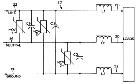
Referring first to Fig. 1, a power conditioning
circuit 20 is connected between line, neutral and ground
conductors 22, 24, 26 and output lines 28, 30 and 32. The
line, neutral and ground conductors may be connected to a
commercial source of power or any other power source. The
CA 02318610 2000-07-19
WO 99/37007 PCTIUS98/27475
-4-
output lines 28, 30 and 32 may be connected to one or more
loads 34.
The power conditioning circuit 20 further includes
first, second and third inductors L1, L2 and L3 connected
in series between the line, neutral and ground conductors
22, 24 and 26 and the output lines 28, 30 and 32. First
through third capacitors C1, C2 and C3 are connected across
the line and neutral conductors 22, 24, the line and ground
conductors 22, 26 and the neutral and ground conductors 24,
26, respectively. Optional metal oxide varistors MOV1,
MOV2 and MOV3 are coupled across the capacitors C1, C2 and
C3, respectively.
Preferably, although not necessarily, the inductance
values of the inductors L1-L3 are equal. Also preferably,
(but not necessarily) the capacitors C1-C3 have
substantially equal capacitance values. Further, the metal
oxide varistors MOV1 and MOV2 must be sized large enough to
dissipate large voltage spikes caused, for example, by a
lightning strike and should, for example, typically have
breakdown voltages on the order of 150-200 volts. In
contrast, the varistor MOV3 resides on the ground leg and,
therefore, is not exposed to large voltage spikes and
should typically have a voltage breakdown level of, for
example, 10 volts.
In operation, transients appearing on any of the line,
neutral and ground conductors 22, 24 and 26 having one or
more frequency components in excess of the nominal
(typically 60 Hz) frequency of the power supplied thereto
are attenuated, by the inductors L1-L3, which have an
increasing impedance with frequency. In addition, these
transients are shunted by the capacitors C1-C3 away from
the load(s) 34. In addition, the metal oxide varistors
MOV1-MOV3 limit the voltage magnitudes appearing across the
line, neutral and ground conductors 22-26.
CA 02318610 2000-07-19
WO 99/37007 PCT/US98n7475
-5-
The actual inductance and capacitance values for the
inductors L1-L3 and the capacitors C1-C3 may be selected so
as to obtain the desired filtering characteristics on the
lines 28-32.
It should be noted that the circuit of 20 of Fig. 1
can be modified by omitting one or more of the elements
therefrom. Thus, for example, one or more of the varistors
MOV1-MOV3 may be omitted, as may one or more of the
capacitors C1-C3 and/or one or more of the inductors L1-L3.
Figs. 2-9 illustrate alternative embodiments of the
present invention wherein elements common to the Figs. are
assigned like reference numerals. Referring first to Fig.
2, one or more of the varistors MOV1-MOV3 may be replaced
by a different voltage limiting element. Thus, for
example, the varistor MOV3 may be replaced by a zener diode
Z1. In a still further embodiment of the present invention
as seen in Fig. 3, any or all of the varistors MOV1-MOV3
may be replaced by combinations of voltage controlling
devices, for example, back-to-back series-connected zener
diodes Z2 and M. Zener diodes positioned in this manner
enable clamping of bidirectional voltage levels. Note that
the zener diodes are not capable of dissipating large
amounts of power, but, instead, are intended to provide
very precise, low level voltage clamping. As a result, in
applications requiring large amounts of power dissipation
MOVs should be used instead of zener diodes. The precise,
low level voltage clamping performed by the zener diodes
enables voltage control for the load ground. In computer
applications low level voltage clamping on the ground leg
is especially advantageous because ground attaches directly
to the microprocessor and is therefore a potential source
of damaging voltage spikes.
Fig. 5 illustrates an embodiment wherein the circuit
20 is provided with back-to-back series-connected zener
CA 02318610 2000-07-19
WO 99/37007 PCT/US98/27475
-6-
diodes Z5 and Z6 which are connected across the lines 28
and 32. If desired in any embodiment, other pairs of back-
to-back diodes may be connected across the lines 28 and 30
or across the lines 30 and 32 (see Fig. 6 which zener
diodes Z7 and Z8 are coupled between the lines 30 and 32).
Fig. 7 illustrates an embodiment wherein back-to-back
zener diodes Z9 and Z10 are connected in series across the
conductors 28 and 30 and back-to-back zener diodes Z11 and
Z12 are connected in series across the conductors 30 and
32.
Referring to Fig. 4, one or more zener diodes or any
other voltage limiting elements may be connected across
point of output lines. Thus, for example, a zener diode Z4
may be coupled across the output lines 28 and 32.
Shown in Fig. 8 is an embodiment wherein an
autotransformer 40 is connected across the lines 28 and 30
to compensate for the voltage drops across inductors Li and
L2 and wherein zener diodes Z13 and Z14 are connected
across the lines 28, 32 and across the lines 30, 32,
respectively.
Fig. 9 illustrates yet another embodiment wherein
back-to-back zener diodes Z15, Z16 are coupled across the
lines 28 and 30, back-to-back zener diodes Z17 and Z18 are
coupled in series across the lines 30 and 32 and back-to-
back zener diodes Z19 and Z20 are coupled in series between
the conductors 28 and 32. In addition, the autotransformer
40 of Fig. 8 is coupled to the lines 28 and 30.
In each embodiment, protection against transients
resulting from line disturbances is afforded in a simple
and inexpensive manner.
Numerous modifications and alternative embodiments of
the present invention will be apparent to those skilled in
the art in view of the foregoing description. Accordingly,
this description is to be construed as illustrative only
CA 02318610 2000-07-19
WO 99/37007 PCT/US98/27475
-7-
and is only for the purpose of teaching those skilled in
the art the best mode of carrying out the invention. The
details of the structure and/or function may be varied
substantially without departing from the spirit of the
invention, and the exclusive use of all modifications which
come within the scope of the appended claims is reserved.