Note: Descriptions are shown in the official language in which they were submitted.
CA 02318667 2000-09-11
1
MONOLITHIC SEMICONDUCTOR PHOTO-COUPLER
INCORPORATING AN OPTICAL FIBER ALIGNMENT GROOVE
BACKGROUND OF THE INVENTION
1. Field of the invention:
The present invention relates to a monolithic
semiconductor photo-coupler device provided for direct alignment of an
optical fiber with a photo-component.
2. Brief description of the prior art:
In the prior art, V-shaped grooves have been currently
used to receive and align optical fibers with photo-components. Examples
are described in the following prior art patent documents:
US 5 355 386 (Rothman et al.) 10/11/1994
US 5 389 193 (Coucoulas et al.)02/14/1995
GB 2 334 788 A (Ojha et al.) 09/01/1999
EP 0 984 533 A2 (Yamauchi) 03/08/2000.
CA 02318667 2000-09-11
2
More specifically, Document GB 2 334 788 A describes
a method by which V-shaped grooves etched in a substrate are aligned
with a planar waveguide core deposited on the substrate.
Document US 5 389 193 describes a method of bonding
an optical fiber in a silicon V-shaped groove simply by applying heat and
pressure. This avoids the use of any potentially contaminating adhesives.
Finally, Document US 5,355,386 describes a
monolithically integrated laser, detector and fiber-receiving channel. The
fiber-receiving channel comprises a V-shaped groove etched through a
wafer structure. The laser and detector are formed of a complex layered
structure.
OBJECT OF THE INVENTION
An object of the present invention is therefore to provide
a simple structure and process of manufacture for a monolithic
semiconductor photo-coupler device, in which a groove and photo-
component are designed for direct alignment of an optical fiber with this
photo-component.
CA 02318667 2003-09-10
3
SUMMARY OF THE INVENTION
More specifically, in accordance with the present
invention, there is provided a monolithic semiconductor photo-coupler
device, comprising a substrate, a groove, a wall of given thickness, and
first and second semiconductor regions. The substrate is made of
semiconductor material, and the groove is made in one face of the
substrate to receive and align an optical fiber. The wall is formed in the
semiconductor material of the substrate in the prolongation of the groove
and transversally to the groove. Also, this wall comprises, on the side of
the groove, a first face generally perpendicular to the groove, and a
second face opposite to the first face. The first and second semiconductor
regions have different electrical properties and are produced in the
semiconductor material on the first and second faces of the wall,
respectively, to form a photo-component.
In this manner, instaAation of an optical fiber in the
groove automatically positions this optical fiber in direct alignment with a
photo-component including the first and second semiconductor regions.
In accordance with preferred embodiments of the
monolithic semiconductor photo-coupler device according to the present
invention:
- the first semiconductor region is a doped region of a first type,
and the second semiconductor region is a doped region of a
second type;
CA 02318667 2003-09-10
4
- the semiconductor material of the substrate comprises silicon,
the doped region of a first type is a p-doped region, the doped
region of a second type is a n-doped region, the p- and n-doped
regions are separated by an intrinsic semiconductor region, and
the p-doped region, the intrinsic semiconductor region and the
n-doped region form a p-i-n photodetector capable of converting
an optical signal from an optical fiber placed in the groove to an
electric signal;
- the monolithic semiconductor photo-coupler device further
comprises a first electrode applied to the substrate in contact
with the first semiconductor region, and a second electrode
applied to the substrate in contact with the second
semiconductor region;
- the face of the substrate in which the groove is made is planar,
the wall further comprises a top edge surface coplanar with the
said one planar face of the substrate, and the first and second
electrodes are applied to both the top edge surface of the wall
and the said one planar face of the substrate; and
the groove is a V-shaped groove, the V-shaped groove extends
on both sides of the wall, and the first and second opposite
faces of the wall are triangular.
The present invention further relates to a method of
CA 02318667 2003-09-10
fabricating a monolithic photo-coupler device from a substrate of
semiconductor material, comprising:
making in one face of the substrate a groove to receive
and align an optical fiber;
5 forming in the semiconductor material of the substrate a
wall of given thickness in the prolongation of the groove and
transversally to this groove, that wall comprising: on the side
of the groove, a first face generally perpendicular to the
groove; and a second face opposite to the first face; and
producing first and second semiconductor regions of
different electrical properties in the semiconductor material
on the first and second faces of the wall, respectively, to
form a photo-component.
According to advantageous embodiments of the
fabrication method:
- the semiconductor material comprises silicon;
- production of the first and second semiconductor regions
comprises doping the semiconductor material on the first face of
the wall to produce a doped region of a first type, for example a
p-doped region, doping the semiconductor material on the
second face of the wall to produce a doped region of a second
type, for example a n-doped region, separating the p- and n-
doped regions by an intrinsic semiconductor region, wherein the
p-doped region, the intrinsic semiconductor region and the n-
CA 02318667 2003-09-10
6
doped region form a p-i-n photodetector capable of converting
an optical signal from an optical fiber placed in the groove to an
electric signal; and
- the fabrication method further comprises applying a first
electrode to the substrate in contact with the first semiconductor
region, and applying a second electrode to the substrate in
contact with the second semiconductor region.
Other objects, advantages and features of the present
invention will become more apparent upon reading of the following non-
restrictive description of a preferred embodiment thereof, given by way of
example only with reference to the accompanying drawings.
BRIEF DESCRIPTION OF THE DRAWINGS
In the appended drawings:
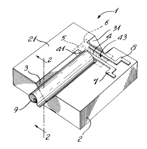
Figure 1 is a perspective view of a preferred embodiment
of the monolithic semiconductor photo-coupler device according to the
present invention; and
Figure 2 is a side elevational, cross sectional view, taken
along line 2-2 of Figure 1, of the monolithic semiconductor photo-coupler
CA 02318667 2000-09-11
7
device of Figure 1.
DETAILED DESCRIPTION OF THE PREFERRED EMBODIMENT
A preferred embodiment of the monolithic semiconductor
photo-coupler device according to the present invention will now be
described. In the appended drawings, the monolithic semiconductor
photo-coupler device is generally identified by the reference 1. Also,
identical elements are identified by the same references in both Figures
1 and 2 of the drawings.
The preferred embodiment of the monolithic
semiconductor photo-coupler device 1 mainly comprises, as shown in
Figures 1 and 2, a substrate 2, a groove 3, a wall 4, first 5 and second 6
semiconductor regions, a first electrode 7 and a second electrode 8.
The substrate 2 is made of semiconductor material. In
the preferred embodiment, silicon is used as semiconductor material. Of
course, it is within the scope of the present invention to use other types of
semiconductor materials, such as GaAs.
The groove 3 is made in a generally planar face 21 of the
substrate 2 to receive an end section of a single-mode or multi-mode
optical fiber 9. As illustrated in Figures 1 and 2, the groove 3 is preferably
V-shaped in cross section. Of course, it is within the scope of the present
CA 02318667 2000-09-11
invention to implement a groove with any other cross section shape. The
V-shaped cross section of the groove 3 has the property of positioning the
optical fiber 9 in precise alignment with the photodetector or other photo-
component which will be described in the following description.
As a non limitative example, the V-shaped groove 3 can
be fabricated with high precision in the face 21 of the silicon substrate 2
by photographic masking and etching. Of course, it is within the scope of
the present invention to use other methods for making this groove 8 in the
face 21.
Although this forms no part of the present invention, just
a word to mention that the end section of optical fiber 9 can be bonded to
the silicon of the substrate 2 by means of an adhesive such as epoxy.
This is only a non limitative example and the present invention is intended
to encompass the use of other methods to bond the optical fiber 9 in the
V-shaped groove 3.
The wall 4 has a given thickness and is formed in the
silicon of the substrate 2 in the prolongation of the groove 3 and
transversally to that groove 3. As illustrated in both Figures 1 and 2, the
wall 4 is formed by making both the V-shaped groove 3 and a V-shaped
groove section 31 coaxial with the groove 3 on the side of the wall 4
opposite to groove 3. This forms a wall 4 having:
on the side of the groove 3, a first triangular face 41
generally perpendicular to V-shaped groove 3;
CA 02318667 2000-09-11
9
on the side of the V-shaped groove section 31, a second
triangular face 42 opposite to the first triangular face 41; and
a generally planar top edge surface 43 coplanar with the
generally planar face 21 of the substrate 2 in which the
groove 3 is made.
The first 5 and second 6 semiconductor regions have
different electrical properties and are produced in the silicon material on
the first 41 and second 42 faces of the wall 4, respectively. More
specifically:
the silicon material is doped on the first face 41 of the wall
4 to produce a doped region of a first type, for example a p-doped
region 5;
the silicon material on the second face 42 of the wall 4 is
doped to produce a doped region of a second type, for example a
n-doped region 6; and
the p- and n-doped regions 5 and 6 are separated by an
intrinsic silicon region 44 (shown in Figure 2).
In this manner, the p-doped region 5, the intrinsic silicon
region 44 and the n-doped region 6 form a p-i-n photodetector capable of
converting an optical signal from optical fiber 9 placed in the groove 3 to
CA 02318667 2000-09-11
an electric signal. Instead of a photodetector, the faces 41 and 42 can be
doped to produce other types of photo-components such as, for example,
a photoemitter component capable of emitting light in the optical fiber 9 for
propagation and transmission through this optical fiber 9.
5
A first electrode 7 is applied to the substrate 2 in contact
with the p-doped region 5, while a second electrode 8 is applied to the
substrate 2 in contact with the n-doped region 6. Those of ordinary skill
in the art will appreciate that the electrodes 7 and 8 can be made of
10 different types of metal and applied by means of conventional techniques
used in the field of microelectronics.
As better shown in Figure 1, the first and second
electrodes 7 and 8 are applied on both the top planar edge surface 43 of
the wall 4 and on the planar face 21 of the substrate 2 for connection to
other circuits (not shown), integrated or not.
Figures 1 and 2 clearly show that mounting of the end
section of the optical fiber 9 in the groove 3 automatically positions this
optical fiber 9 in direct alignment with the photodetector including the p-
doped region 5, the intrinsic silicon region 44 and the n-doped region 6.
Those of ordinary skill in the art will also appreciate that
the structure of the groove 3 and wall 4 assembly and the fabrication of an
photo-component by simply doping the opposite faces of the wall 4 result
in a very simple, easily manufactured structure for the monolithic
semiconductor photo-coupler device 1.
CA 02318667 2000-09-11
11
Although the present invention has been described
hereinabove by way of a preferred embodiment thereof, this embodiment
can be modified at will, within the scope of the appended claims, without
departing from the spirit and nature of the subject invention.