Note: Descriptions are shown in the official language in which they were submitted.
CA 02318721 2000-09-13
_.
PROCESS AND DEVICE FOR THE THERMAL CONDITIONING OF
ELECTRONIC COMPONENTS
The present invention tackles the problem of the
thermal conditioning of electronic components, and has
been developed with particular regard to possible
application to the temperature control of semiconductor
laser modules.
In this field of application it is important to
ensure the stability of the operating conditions. This
is particularly true of wavelength division
multiplexing (WDM) systems, and especially for high
density (DWDM) systems, where it is necessary to
control the temperature of the laser accurately, since
the emission frequency depends directly on the
temperature of the component, with a coefficient of
proportionality of the order of approximately - 10
GHz/°C. Since rather small channel spacings, of the
order of 50 GHz for example, are used in the most
recent systems, it is necessary to ensure temperature
stability in a range of values below 1°C.
To achieve the necessary temperature
stabilization, circuits have been developed which use a
temperature-sensitive resistor (for example an NTC
thermistor) as the sensor and a thermoelectric cell
(Peltier cell) as the temperature control or
conditioning element. These circuits can be used to
stabilize the temperature of the sensor within a range
of 0.5°C without any special circuit arrangements.
The control circuit regulates the current in the
Peltier cell in such a way as to keep the sensor
reading equal to a reference reading. However, since
the position of the temperature sensor does not exactly
coincide with that of the laser diode (referred to
simply as the "laser" in the following text), there may
be a temperature difference between the laser and the
sensor, which depends on the structure of the package
CA 02318721 2000-09-13
- 2 -
containing the component. Consequently, the actual
temperature of the laser can vary considerably,
particularly with a change in external temperature,
despite the correct operation of the temperature
control. While the temperature of the sensor is kept
constant by the control circuit, there may be,
depending on the particular structure of the package,
either conditions in which the actual temperature of
the laser rises with an increase in the temperature of
the package, or conditions - most frequently
encountered in commercial components - in which the
temperature of the laser falls with an increase in the
external temperature.
A situation of this type is shown schematically in
Figure 1 of the attached drawings, which shows three
parallel vertical lines, each corresponding to an ideal
temperature scale. Moving from left to right, we find
three scales of possible temperature values,
corresponding, respectively, to the package, the
temperature sensor (thermistor) and the laser: thus it
can be seen that, even if the temperature of the sensor
is kept constant, the variations of temperature in the
package cause corresponding variations of the
temperature of the laser and therefore a variation of
the operating conditions of the laser.
The paper by A. Adachi, S. Kaneko, J. Yamashita
and K. Kasahara, "Low-frequency drift laser-diode
module for a wide temperature range using two
thermistors", published on pages 109 and 110 of the
OFC/IOOC '93 Technical Digest describes a solution
(taken as the model for the preambles of Claims 1 and
7) in which two thermistors, one located in proximity
to the laser and the other at a certain distance from
the first thermistor, are positioned on the base plate
carrying the laser. The different temperatures read by
the two thermistors are used to produce a kind of
CA 02318721 2000-09-13
- 3 -
estimate or interpolation of the temperature difference
present between the first thermistor and the laser.
Even without a discussion of the real
effectiveness of a solution of this kind, it is
immediately apparent that it necessarily entails the
provision of the second thermistor during the
manufacture of the package comprising the laser. This
solution is therefore not applicable to commercial
components, which are supplied already sealed into
their packages, or, in other words, when it is no
longer possible to modify the base plate of the
component.
The object of the present invention is to overcome
the aforesaid disadvantage with a solution which is
also applicable to commercial components (and therefore
to those already enclosed in their packages), without
the need to make modifications inside the package, and
which, in all cases, provides very precise temperature
control.
According to the present invention, this object is
achieved by means of a process having the
characteristics claimed specifically in the following
claims.
The invention also relates to the corresponding
device.
Briefly, the solution according to the invention
provides a control circuit which is designed to make
the reading of the sensor equal to that of a reference
made to vary as a function of the external temperature,
measured by another sensor preferably located in
contact with the package.
In general, the references made - both here and in
the following claims - to the temperature conditioning
of electronic components are intended to allow for the
fact that the possible range of application of the
invention is not in any way restricted to the cooling
of a laser module by means of Peltier cells, although
CA 02318721 2000-09-13
- 4 -
reference has been and will be made to this application
by way of example.
In particular, the solution according to the
invention is suitable for use for a thermal
conditioning (temperature control) operation intended
for cooling a component which tends to heat up during
operation and/or to heat a component whose temperature
- for a wide range of reasons - is to be raised (for
example, in order to obtain a fixed operating
temperature even in the presence of a lower external
temperature). Clearly, however, it is possible that, in
many case, the same component may be concerned, being
intended to be alternatively cooled and heated in the
presence of different environmental and/or operating
conditions. The means of thermally conditioning the
component (shown schematically here in the form of a
Peltier cell, intended primarily to cool the component)
can therefore be produced and/or controlled (according
to entirely known principles) in such a way that the
component can be heated, in addition or as an
alternative to the cooling.
This component can consist of a component of any
kind or nature.
The invention will now be described, purely by way
of example and without restrictive intent, with
reference to the attached drawings, in which:
- Figure 1, showing the intrinsic disadvantages of
the solutions according to the known art, has already
been discussed,
- Figure 2 shows, in the form of a block diagram, an
example of the embodiment of a device according to the
invention,
- Figure 3 shows, in a format essentially similar to
that of Figure 1, the operating principles of the
solution according to the invention,
- Figures 4a and 4b show the operating
characteristics of a conventional device for the
CA 02318721 2000-09-13
- 5 -
temperature conditioning of an electronic component
such as a semiconductor laser, and
- Figures 5a and 5b show the results which can be
achieved with the device according to the invention in
the temperature conditioning of the electronic
component to which Figures 4a and 4b relate.
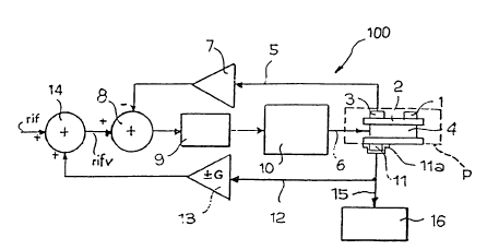
In the diagram in Figure 2, the circuit according
to the invention is indicated as a whole by 100. The
numeric reference 1 indicates an electronic component
consisting, in the illustrated example of embodiment,
of a semiconductor laser, such as a distributed
feedback (DFB) laser. The laser 1 is mounted on a base
plate 2 together with a temperature sensor 3. The
latter typically consists of a thermistor mounted on
the plate 2 in proximity to the laser 1.
The numeric reference 4 indicates a thermoelectric
cell (Peltier cell) acting as a means of thermal
conditioning of the laser 1 with the effect of cooling
the laser. Finally, the reference P indicates the
package which encloses the various elements mentioned
above.
The set of parts described corresponds in a
general way to a commercially available component,
sealed inside the package P. This package may have
different configurations, which can produce different
behaviours in terms of the ratio between the
temperature of the package P and the temperature of the
laser 1. In particular, it may happen that the
temperature of the laser 1 decreases with an increase
in the external temperature (behaviour illustrated in
Figure 1), or that the temperature of the laser 1
increases with an increase in the external temperature;
all this is true even if the temperature of the
internal sensor (sensor 3) remains constant.
The package P is also provided with pins or
similar contact elements which enable it to be
CA 02318721 2000-09-13
- 6 -
connected electrically to the other elements of the
circuit.
Some of these pins (not explicitly shown in the
drawings) correspond to the control lines for the laser
1 and to the various functions of power supply to the
components associated with it.
Additionally, at least two other pins
corresponding to the lines indicated by 5 and 6
respectively are provided.
The line 5 is a line on which the output signal of
the sensor 3 is present. This output signal
(essentially a signal indicating the temperature of the
sensor 3) is sent to the input of a variable-gain
element 7, such as an amplifier, whose output signal is
sent to the inverting input of an addition node 8. A
reference signal rifv, generated according to
principles illustrated in greater detail below, is
supplied to the non-inverting input of the node 8.
The output signal of the node 8, corresponding to
a deviation or error signal, indicating the difference
between the reference signal rifv and the temperature
signal generated by the sensor 3 (scaled by the value
of the gain of the element 7), is sent to the input of
a proportional integral circuit 9. The output signal of
the circuit 9 is used to drive a control circuit 10
designed to generate the power supply current for the
thermoelectric cell 4.
The set of elements indicated by the references 5
to 10 also corresponds to a solution known in the art:
in practice, this is a feedback loop whose function is
to keep the temperature level measured by the sensor 3
constant at a predetermined value (determined by the
reference signal rife applied to the non-inverting
input of the node 8).
As stated in the introductory part of the
description, this temperature control action, since it
relates to the sensor 3 (whose position, although close
CA 02318721 2000-09-13
-
to that of the laser 1, is not coincident with it),
cannot ensure that the temperature of the laser 1 is
kept at a constant level. The operating conditions of
the laser 1 are therefore affected by the variations of
the external temperature, particularly at the package
P.
In the solution according to the invention, the
laser module is associated with a further temperature
sensor 11, typically positioned on the package P or, in
any case, in such a way as to make it sensitive to the
external temperature.
For more satisfactory operation of the circuit,
the external sensor 11 must provide a linear indication
of the temperature. A suitable sensor may be the LM 35
temperature sensor made by National Semiconductors.
Preferably, the sensor 11 is located on the
package P, with an arrangement promoting conditions of
low resistance to heat exchange between the sensor 11
and the package P. For example, it is possible to
secure the sensor 11 to the package P by means of a
bracket lla, or use alternative solutions such as an
adhesive joint. All this is true without prejudice to
the fact that the application of the further sensor 11
does not require any particular modification to be made
to the package P, and therefore the invention is
applicable to any commercial component.
The output signal of the sensor 11, which
constitutes another temperature signal, is sent by
means of a line 12 to a further variable-gain element
13, usually similar to the element 7. The signal
leaving the element 13 is supplied to one of the inputs
of a further addition node 14. The node 14 has another
input to which a reference signal, called rif, is
applied. The output signal of the node 14 forms the
reference signal rifv supplied to the input of the node
8 of the control loop described above.
CA 02318721 2000-09-13
- g _
The reference signal rif is set in such a way that
it determines the actual temperature at which the laser
1 is to be maintained.
The signal supplied from the sensor 11 (through
the line 12 and the variable-gain element 13) is
applied to the other input of the node 14 in such a way
as to induce in the variable reference signal rifv
variations representing the temperature variations
measured by the sensor 11. Thus the reference signal
rifv applied to the input of the node 8 varies and
causes a corresponding variation in the temperature at
which the sensor 3 is maintained, while on the other
hand the temperature of the laser 1 is kept constant.
All this is true although the sensor 3 and the laser 1
are located at a certain distance from each other.
These modes of operation are shown schematically
in Figure 3, whose arrangement reproduces the
arrangement of Figure 1 described above.
Preferably, the output signal of the sensor 11,
taken from a line 15, is also sent towards a thermal
alarm module 16. The latter is capable of detecting the
condition in which the temperature measured by the
sensor 11 has reached a threshold level corresponding
to a temperature beyond which reliable operation of the
laser 1 can no longer be counted on. In these
conditions, the module 16 can operate in such a way as
to take the action considered necessary (turning off
the laser 1 and/or emitting a warning signal towards
the exterior).
The operation of calibrating the gain of device 13
can be carried out by initially making the circuit
operate in a conventional way, in other words with the
external temperature sensor (sensor 11) turned off.
In these conditions, it may happen that, for
example, when the temperature external to the package P
is varied over a range from 10°C to 60°C, the
temperature of the thermistor 3 remains constant
CA 02318721 2000-09-13
_ g _
(within 0.1°C, for example), while the emission
frequency of the laser 1 varies, for example, by
approximately 15 GHz, corresponding to a variation of
1.5°C in the real temperature of the laser, as shown in
the diagrams in Figures 4a and 4b.
The reported data relate to a commercial DFB laser
mounted on a board subjected to heat cycles between
10°C and 60°C, in both directions, with a rate of
1°C/min., using a heating chamber. The figures show, as
functions of the ambient temperature (the horizontal
scales in both diagrams), the variations of the
temperature and consequently the resistance of the
thermistor 3 (the vertical scale on the right and left
respectively in diagram 4a) and the frequency of the
optical signal emitted by the laser 1 (the vertical
scale in diagram 4b) measured by means of a wavemeter.
The variations of the frequency of the optical
signal are evident.
When the difference between the temperature of the
internal sensor 3 and the actual temperature of the
component to be controlled (the laser 1) is known, it
is then necessary to set a reference value rifv such
that this difference is compensated.
This procedure makes it possible to calculate (and
regulate) the gain of the element 13 with sufficient
precision: this value can, however, be additionally
optimized in an experimental way by observing the
residual drift of the emission frequency of the laser
1.
The slope of the "Frequency vs. external
temperature" curve (Fig. 4b) sets the sign (inverting
or non inverting) of the gain of device 13.
The diagrams in Figures 5a and 5b show the
experimental results achieved with the circuit shown in
Figure 2 in the same test conditions as those used for
plotting the diagrams in Figures 4a and 4b. In this
case, the circuit of Fig. 2 was made to operate with
CA 02318721 2000-09-13
- 10 -
the sensor 11 connected in such a way that it could
intervene in the operation of the circuit according to
the criteria described above.
In this case also, the figures show, as functions
of the ambient temperature (the horizontal scales in
both diagrams), the variations of the temperature and
consequently the resistance of the thermistor 3 (the
vertical scale on the right and left respectively in
diagram 5a) and the frequency of the optical signal
emitted by the laser 1 (the vertical scale in diagram
5b) measured by means of a wavemeter.
The stabilizing effect on the emission wavelength
(the maximum deviation found is of the order of 800
MHz) is clearly apparent.
Naturally, the details of construction and the
forms of embodiment can be varied considerably from
what has been described and illustrated, provided that
the principle of the invention is retained, without
departing from the scope of the present invention.