Note: Descriptions are shown in the official language in which they were submitted.
CA 02318866 2000-07-21
WO 99/38271 PCT/US99/00146
1
SYSTEM FOR DISCRETE DATA TRANSMISSION
WITH NOISE-LIKE, BROADBAND SIGNALS
BACKGROUND OF INVENTION
- 1. Field of the Invention
The present ins-ention relates to broadband communication systems and
particularly to systems for transmission and reception of pseudorandom noise
and spread
spectrum signals, and to code division multiple access systems with
application to
satellite and terrestrial communications.
2. Description of the Related Art
Spread spectrum systems have been used for many years in digital
communications. A spread spectrum signal consists of a baseband message signal
modulated onto a carrier and thereafter spread in frequency by a pseudorandom
noise
sequence ("PN sequence" or "PNS"), independent of the message signal itself.
The
receiver then recovers the message signal by using a replica of the PN
sequence. The
main advantages of spread spectrum systems are good interference and noise
rejection,
low power density, ability to access multiple channels (such as in code
division multiple
access (CDMA) systems), high resolution ranging, and message protection. The
ratio of
the bandwidth of the PNS to that of the message signal, called the processing
gain,
determines the merit of the system.
Typical block diagrams of a spread spectrum transmitter and receiver are found
in J. K. Holmes, Coherent Spread SF~ectrum Systems (Wiley 1982), and
reproduced as
Figures 1 a and 1 b. In the transmitter in Figure 1 a, a digital message
signal transmitted
at bit rate B is provided to coder 100. This coder encodes the data bits into
codewords
for transmission and can be a block coder or a convolutional coder as
described in G. C.
Clark and J. B. Cain, Error-Correction Coding for Dieital Communications
(Plenum
Press 1981 ). Carrier frequency generator 112 generates a carrier frequency
signal that
is modulated by the coded signal in earner modulator 106. PNS modulator 108
then
CA 02318866 2000-07-21
WO 99/38271 PCT/US99/00146
2
further modulates (or spreads) the modulated carrier signal with a PN sequence
from PNS
generator 128. The PNS is a digital signal made up of "chips" and whose chip
interval
or chip period is much smaller than the data bit period (thus the bandwidth of
the PN
sequence is much greater than that of the data signal). The resulting signal
is amplified
by amplifier 130 and transmitted by antenna 140. .
As depicted in Figwe lb, the transmitted signal is received by antenna 152 and
amplified by amplifier 154. Because the phase and frequency of the received
signal is
unknown, the received signal must be acquired and tracked to establish phase
synchronization. The received signal is provided to tracking and acquisition
(T&A)
synchronism device 164 which contains a PNS generator that generates a replica
of the
PNS that was used in the transmitter. In the acquisition stage, a coarse
alignment
between the replicated PNS and the received signal is performed using serial
and/or
sequential search, sequential estimation, universal timing, or matched filter
algorithms.
These techniques are described in various,references, one of which is R. C.
Dixon,
(Whey 1994). The acquisition
stage brings the replicated PNS and the received signal within half a chip
interval of each
other. Once the received signal is acquired, the two signals are tracked,
generally using
a delay-lock loop. ,~,g,,g" J. J. Spilker, ~eital Comm~cadon b, at llit
(Prendce
Hall 1977). Once synchronized, T&A synchronism device 164 outputs the in-phase
PNS
to PNS demodulator 156 which demodulates (despreads) the received signal. The
despread signal is provided to carrier restoration and phasing module 166
which provides
a local oscillator signal which is phase-synchronized to the carrier signal.
The local
oscillator signal is used to demodulate the despread signal in coherent
detector 158
producing a baseband coded data signal. The baseband signal is provided to
clock
frequency extractor 168 to extract the clock signal, which in twn is provided
to decision
circuit 160 which can be implemented as an integrator over a bit period to
determine
whether a code bit is a one or a zero. Decision circuit 160 provides squared-
up digital
data code bits to frame synchronization device 170 and noise-immune decoder
162.
Frame synchronization device 170 uses the clock signal from clock frequency
extractor
168 to extract the word (or frame) timing from the digital data code bits to
derive a frame
CA 02318866 2000-07-21
WO 99/38271
3
PCT/US99/00146
synchronization signal that is used to decode the digital data signal in noise-
immune
decoder 162 to recover the original digital message signal.
The main problem associated with this spread spectrum system is that the
receiver
contains a sequence of modules - tracking and acquisition 164, carrier
restoration 166,
clock extraction 168, and frame synchronization 170 - each of which must wait
for the
previous module to acquire synchronization before being able to start its own
synchronization process. The throughput of the system is therefore dependent
upon each
of the modules and can suffer if only one is slow to synchronize. Another
problem is that
the receiver requires four separate modules that duplicate some functions,
i.e. phasing is
performed in T&A synchronism device 164 and in carrier restoration and phasing
module
166, and clock frequency extractor 168 is needed because the phasing performed
by T&A
synchronism device 164 is not accurate enough to clock decision circuit 160.
An improved prior art system is depicted in Figures 2a and 2b. In the
transmitter
in Figure 2a, coder 204, carrier modulator 206, PNS modulator 208, carrier
frequency
generator 212, amplifier 230, and antenna 240 perform as in Figure 1 a. New to
this
transmitter is a second output from PNS generator 228 that provides a pulse
corresponding to the beginning of each period of the PNS to switch 222 and
period
multiplier 210. Switch 222 then provides a clock to buffer memory 202 to
synchronously
clock the data bits into coder 204. The multiplication factor in period
multiplier 210 is
variable; thus, the period of the data bits clocked through to coder 204 can
vary but is
always an integral multiple of the PNS period. The use of this relationship
between the
data bit period and the PNS period enables the system to eliminate the clock
frequency
extractor from the receiver in Figure 2b. In its place are switch 268 and
period multiplier
272 which detect the clock, but do so at an earlier stage than in Figure 1 b
because period
multiplier 272 is directly connected to T&A synchronism device 264. The rest
of the
receiver works as before; thus, when the baseband coded data signal reaches
decision
circuit 260 from coherent detector 258, clock synchronization has already been
performed and only frame synchronization remains to be performed.
One advantage of this system over the prior art system in Figures 1 a and 1 b
is that
the circuitry is simpler because the clock frequency extractor is more complex
than the
switches and multipliers in the transmitter and receiver that substitute for
the clock
CA 02318866 2000-07-21
WO 99/38271
4
PCTNS99/00146
frequency extractor. Another.advantage is that the receiver operates more
quickly
because clock synchronization is performed simultaneously with carrier
restoration.
However, there are still problems with this spread spectrum system. First, the
bulk of the receiver still operates serially, reducing receiver throughput.
Second, the
frame synchronization device takes time to generate a frame synchronization
signal and
has low noise immunity due to the possibility of elementary signal distortion
inside the
frame synchronization signal, especially when communicating with moving
objects,
~~ ~y ~s° ~ ~~ sort-ups ~ fi'ame synchronization device 270 when there
is low
redundancy in the frame synchronization signal. Third, the operation of this
type of
system is limited when the PNS period is on the older of several chips,
because the
discrete nature of the spectrum radiated by the transmitter decreases the
bandwidth of the
sy' 1°~'"~g c~el capacity when operating in code division mode and
reducing
noise immunity and interference rejection. These drawbacks may be lessened by
lengthening the PNS period, which creates a more continuous spectrum, but that
significantly complicates the receiving equipment, lengthens acquisition and
trackin
g
time, and worsens correlation functions in the receiver. This lowers the
effective signal
base which in turn reduces channel capacity and interference rejection.
The present invention addresses the shortcomings in these prior art systems.
Thus, it is an object of the present invention to provide a spread spectrum
system with
better noise immunity, faster receiver synchronization, simpler electronics,
and increased
channel capacity and interference rejection.
SUMMARY OF THE INVENTION
~e ~~'°v~ sP~ spectrum system includes a transmitter and a receiver.
The
transmitter includes a data channel, a control channel (also called a pilot
channel), a
carrier and clock frequency generator, and two PNS generators - one generating
a bit
PNS and the other generating a word PNS. Both PNS generators output pulses
corresponding to the beginning of their respective PNS periods and provide
those pulses
to the data channel to time the data bits and the codewords into which the
data bits are
converted. The coded data signal modulates a carrier and then the modulated
signal is
spread by the bit PNS. The control channel controls the timing of the two PNS
CA 02318866 2000-07-21
WO 99/38371
PCTNS99/00146
generators and the changing of the forms of the two PN sequences. Control data
are used
to modulate a quadrature-ple c~er, and this modulated quadrature-ple signal is
spread by the word PNS. The spread data signal is added to the spread
quadrature control
signal and transmitted. The receiver includes a data channel, a control
channel, and a
5 data channel tracking and acquisition (T&A) module. The control channel
includes a
T&A and carrier frequency restoration module that uses a replica of the word
PNS to
produce the in-phase and quadrature-phase carrier, a pled version of the word
PNS,
and a word synchronization signal. The quadrature-phase carrier and the word
PNS are
respectively used to demodulate and despread the control channel portion of
the received
signal. The control signals are demodulated and are used to change the forms
of the PN
sequences in the two T&A modules. The in-phase carrier is used to demodulate
the data
channel portion of the received signal, and the word synchronization signal is
used to
acquire and track the demodulated received data signal and to provide a phased
version
of the bit PNS to the receiver data channel to despread the received signal.
The data.
channel T&A module also provides a bit synchronization signal to the data
channel for
decision-making and decoding.
This improved spread spectrum system eliminates the need for a, separate clock
frequency extractor or frame synchronization device, simplifying the receiver
structure
and making it less expensive. The receiver operates more efficiently because
the bit
synchronization signal and the word synchronization signal are derived more
easily and
at an earlier stage than in the prior art. Faster receiver processing allows
for higher bit
rates. Frame synchronization is more accurate thus increasing noise immunity
and the
system's ability to communicate with moving objects. Changing the forms of the
PN
~lu~~ yes the spectrum more continuous allowing for better noise and
interference
' 25 rejection and higher channel capacity.
BRIEF DESCRIPTION OF THE DRAWINGS
Figure 1 a is a block diagram of a prior art spread spectrum transmitter;
Figure 1 b is a block diagram of a prior art spread spectrum receiver;
Figure 2a is a block diagram of a second prior art spread spectrum
transmitter;
Figure 2b is a block diagram of a second prior art spread spectrum receiver;
CA 02318866 2000-07-21
WO 99/38271
6
PCTNS99/00146
Figure 3 is a block diagram of the transmitter of the improved spread spectrum
system;
Figure 4 is a timing diagram of the signals within the transmitter;
Figure 5 is a second timing diagram of the signals within the transmitter
after the
PNS forms have been changed; and
Figure 6 is a block diagram of the receiver of the improved spread spectrum
system.
DETAILED DESCRIPTION OF THE INVENTION
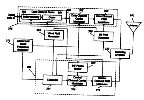
Figure 3 is a block diagram of an improved transmitter in accordance with the
present invention. It includes two transmitter channels, data. channel 310 and
control
channel 322. In addition, there are provided carrier and clock frequency
generator 312,
bit PNS generator 328, word PNS gener for 324, summing amplifier 330, and
transmitting antenna 340. Data channel 310 includes data channel coder 300,
data
channel carrier modulator 306 and data channel PNS modulator 308. Control
channel
322 includes phase shifter 320, controller 314, control channel carrier
modulator 316, and
control channel PNS modulator 318.
As in the prior art of Figure 2a, bit PNS generator 32$ has two outputs, one
output
provided to data channel PNS modulator 308 generating a PN sequence with N
chips per
PNS period at chip rate P,, the other output provided to data channel coder
300 providing
a pulse at the beginning of each bit PNS period. In accordance v~~ ~e
invention, there
is a second PNS generator, word PNS generator 324, that generates a second
pseudorandom noise sequence. Word PNS generator 324 also has two outputs, one
output providing M chips per PNS period at chip rate P2 to control channel PNS
modulator 318, and the second output providing a pulse at the beginning of
each word
PNS period to data channel coder 300. The two PN sequences can be generated by
any
known method, the most common of which uses a shift register. ~ S, W.
Golomb, shift ReQi~rPr eP""o""e~ Aegean Park press 1982) or R. C. Dixon,
~~ Svstemc y:~th (~o mPn~;m ~ ".";"'~ (Wiley 1994). Carrier and clock
frequency generator 312 provides a carrier frequency suitable for RF
transmission. It
also outputs timing signals to the control channel which in turn provides the
clock for
CA 02318866 2000-07-21
WO 99/38271
7
PCT/US99/00146
word PNS generator 324 and bit PNS generator 328. Alternatively, instead of
using.
controller 314 to clock the PNS generators, carrier and clock frequency
generator 312 can
directly provide separate clock outputs to the two PNS generators.
Digital data, at bit rate B, is provided to data channel coder 300. The choice
of
data rate B is not critical, although it is related to the bandwidth of the
system by the
k~P
equation B = n . N , where k is the number of data bits in a data word, n is
the number
of symbols into which the k bits are coded and transmitted, P, is the bit PNS
chip rate,
and N is the number of chips in each period of the bit PNS. P, is typically in
the range
of 0.8dF to 2dF where dF is the bandwidth of the system, and is more typically
equal
to dF. Although N can be any number, it is normally 2''' or 2', where 1 is an
integer.
Typical values of N are therefore 31, 32, 63, 64, 127, 128, 255, 256, etc.
Every k data
bits at the input to data channel coder 300 are converted into n symbols
output from data
channel coder 300. The variables n and k are related by n s k, with typical
values of n
in the range ~ 2~ < n < 3k, although in a non-redundant system, n = k. Thus,
for
P,=dF,lV=3l,andn=3k (or 3~)
equivalently, if N = 63 and n = , B = 0.01- dF. In
2
such cases, taking dF = 1, 5, 10, 20, 250 MHz, then B = 10, 50, 100, 200, 2500
kb/s,
respectively. In a typical system, dF and B are chosen first, and N and P, are
then
determined based on B, n, and k. Thus, the bit PNS period, p , is equal to the
length
of each of the code symbols from data channel coder 300 which equals k It is
n ~ B
preferable to select N not less than 63 on the low side. On the high side,
selection of N
is limited by the acquisition time in the receiver, so it is also preferable
not to select N
too large.
Data channel coder 300 comprises buffer memory 302 and coder 304. Buffer
memory 302, which is typically a memory register with a capacity of k bits,
matches the
rate of the input data to the rate of the symbols output from coder 304.
Buffer memory
302 is clocked by the output pulses from bit PNS generator 328. Coder 304,
which can
perform either block coding or convolutional coding, is clocked by pulses from
word
PNS generator 324. (If convolutional coding is chosen, frame synchronization
for the
input data will be executed.) Thus, for the system with input data rate B, the
symbol rate
CA 02318866 2000-07-21
WO 99/38271
8
PCT/US99/00146
provided by buffer memory 302 (and coder 304) is B ~ . In the specific case
where n = k;
coder 304 is no longer needed, but buffer memory 302 is still needed to retain
the phase
coincidence between the input data bits and bit PNS generator 328. The length
of a
codeword is equal to the word PNS period. For a word PNS period containing M
chips
and a word PNS chip rate of P2, the word PNS period
,B 'n = B, and
PI n
therefore P1 = M ~ ~ . If P, = p1, den M = n ~ N. Setting P, = Pz is prefen~ed
in order
to equalize the bands in the in-phase (data) and quadratuze-phase (contml)
channels.
However, P, can also be greater or less than P1. If P, > Ps, then n ~ N > M;
if P, < p1,
then n ~ N < M, It is even possible that M = N, i.e. the lengths of the bit
PNS and the
word PNS are the same.
After coding, the symbol stream is provided to data channel modulator 306 to
modulate the carrier signal. The modulator can use any type of modulation,
however
binary phase shift keying (BPSK) or differential phase shift keying (DPSK) are
,preferable. The modulated output is provided to data channel PNS modulator
308 where
it is spread by the bit PNS.
Exemplary waveforms at various points in the tt~, ~ ~o~ ~ Figure 4.
That figure depicts the case where there are five bits per data word with no
redundant
coding (n = k = 5) (i.e. International Telegraphy Code ITC-2), N= 7, and p~ =
P2 so that
M = n ~ N = 35. Wavefonn 4(a) shows the pulse output of bit PNS generator 328
that
clocks buffer memory 302. Waveform 4(b) shows the data signal 1 O1 Ol at the
input to
data channel modulator 306. Waveform 4(c) shows the carrier signal at the
input to data
channel modulator 306. Waveform 4(d) shows the modulated output fibm data
channel
modulator 306. Waveform 4(e) shows the output of bit PNS generator 328 as a 7-
bit
Barker code, 1110010, repeated each period. Wavefornl 4(fj shows waveform 4(d)
modulated by the bit PNS. Waveform 4(f) is the data channel signal and is
provided to
summing amplifier 330 to be added to the control channel signal.
Control channel 322 operates in a manner similar to that of the data channel
except that its bit rate is lower than that of the data rate and the channel
is modulated with
the quadrature-phase carrier. More specifically, carrier and clock frequency
generator
312 provides clock rate B~ to controller 314. This clock rate is related to
the chip rate PI
CA 02318866 2000-07-21
WO 99/38271
9
PCT/US99/00146
by the same mlation as in data c>~el 310 i.e. P _ pit ~ B _ B
> > 1 ~ . In ~1 X1322, B - -
k
(i.e. B~ < B), ~~ p? = M . ,g~, Controller 314 synchronizes bit PNS generator
328 and
word PNS generator 324 with a pulse rate equal to B~ (= ~ ). ply, ~ntroller
314 sends
instructions to the two PNS generators and changes the forms of the two PN
sequences
by dictating different sequences. For example, if the bit PNS is 1110010 (as
in Figure
4(e)), controller 314 might change it to its inverse 0100111 (see Figure
5(e)). Similarly,
if the word PNS is 1101110 0011111 0111000 0000001 0110010 (see Figure 4(h)),
controller 314 might change it to its inverse 0100110 1000000 0001110 1111100
0111011 (see Figure 5(h)). There are many possible forms that the two PN
sequences
may take on, and they are preprogramni~ by ~e system designer. However, only
the
sequences themselves change - the chip rate, the sequence length, and the
phase
relationship between the two PNS generators do not change.
This change of PNS forriis makes the PN sequences more random and thus
increases interference rejection and channel capacity. Without changing forms,
the
spectrum of the bit PNS becomes discrete because of periodic repetition of the
same
PNS. This decreases the processing gain of the system (see. e.gs, R, C. Dixon,
(Figs. 2.7, 3.29) (Wiley T984)). If the
PNS forms change at the frequency of the codeword repetition rate, ~ , a
specific bit
PNS well only be transmitted n times dunrlg the codeword and then the PNS will
change.
Thus the signal spectrum will begin to look continuous, and processing gain
will increase
because it is directly proportional to the bandwidth of the system. The
specific amount
of the increase in processing gain is determined experimentally, not
analytically.
Because the PNS forms must also change in the receiver, the control channel
instructions are provided to control channel carrier modulator 316. The
instruction bits
modulate the carrier signal from carrier and clock fiequency generator 312,
the output of
which has been phase shifted 90° in phase shifter 320. Although phase
shifter 320 is
depicted in Figure 3 as being part of control channel 322, it could just as
easily be a
separate module or could be part of carrier and clock fi~equency generator
312. The
resulting quadrature-phase modulated carrier is further modulated by the word
PNS in
control channel PNS modulator 318 and the resulting signal is provided to
summing
CA 02318866 2000-07-21
WO 99/38271
PCT/US99/00146
amplifier ~ 330 to be combined with the data channel modulated signal and then
transmitted via antenna 340.
Exemplary control channel waveforms are shown in Figure 4. Waveform 4(g)
shows the output pulses of word PNS generator 324. Because the clock rate
controlling
5 controller 314 is the same as the output pulse rate of word PNS generator
324, the
controller output bits are not shown. Waveform 4{h) shows the word PNS having
35
chips per clock period, corresponding to the pulses of word PNS generator 324,
as
described above. Waveform 4(i) shows the carrier signal at the input to
control channel
modulator 316 (it is phase shifted 90° from waveform 4(c)). Waveform
4(j) shows the
10 modulated output from control channel carrier modulator 316 and is the
control channel
signal provided to summing amplifier 330 to be added to the data channel
signal.
Figure 5 depicts the waveforms at the same points as in Figure 4, but the PNS
forms have been changed. Waveforms 5(a), 5(c), S(g), and 5(i) are the same as
wavefomls 4(a), 4(c), 4(g); and 4(i), respectively. Waveform 5(b), the input
data signal,
is now 11011, thus changing waveform 5(d), the output signal from data channel
carrier
modulator 306. Wavefonn 5(e) is the inverse PNS of waveform 4(e), and waveform
5(f)
shows the resulting data channel output signal. Waveform 5(h) shows the
changed form
of the word PNS as described earlier, and waveform 5(j) shows the control
channel
output signal.
Figure 6 is a block diagram of the receiver of the improved spread spectrum
sy' ~ m me tl'ansmitter, the receiver comprises two channels, data channel 630
and
control channel 640. In addition, there is also data channel tracking and
acq~sition
(T&A) module 616, amplifier 604, and receiving antenna 602. Data channel 630
includes coherent detector 606, data channel PNS demodulator 608, decision
circuit 610,
and noise-immune decoder 612. Control channel 640 further comprises control
channel
T&A and carrier frequency restoration module 614, control channel demodulator
618,
and receiver controller 620.
Receiving antenna 602 and amplifier 604 operate as in the prior art systems of
Figures 1 b and 2b. The received signal is first provided to control channel
T&A and
carrier frequency restomhon module 614. As in the prior art, the acquisition
circuitry of
this module includes a PNS generator that produces the same PNS as in the
transmitter.
CA 02318866 2000-07-21
WO 99138271
11
PCT/US99/00146
In the present invention, only the word PNS is used in the acquisition
circuitry in control
channel T&A module 614. (The bit PNS is used in data channel T&A module 616.)
Besides this feature, acquisition is accomplished as in prior art systems.
Once the
received signal is acquired, tracking proceeds as in the prior art, generally
using a delay_
lock loop. In addition, carrier restoration is also performed by control
channel T&A
module 614, just as in the prior art, typically using a phase-locked loop. ~
A, J.
Viterbi, (Addison-Wesley 1995):
These processes yield four outputs - a correctly phased version of the word
PNS, a
quadrahu'e-phase version of the carrier signal, an in-phase version of the
carrier signal
, (formed by shifting the quadrat~_pversion 90°), arid a word
synchronization signal
derived from the taming of the word PNS. In the specific case of M = n ~ N,
then the
word synchronization signal and the phased version .of the word PNS have the
same
p~~. The phased PNS and the quadrature_p~ her signal are provided to control
channel demodulator 618 to despread the word PNS from the received signal. The
signal
' 15 provided to controller 620 from control channel demodulator 618 consists
of the control
signals needed to change the PNS forms in the receiver. Using the word
synchronization
signal from control channel T&A module 614, controller 620 provides control
instructions to control channel T&A module 614 and to data channel T&A module
616.
5~~~~uslY, the in-phase version of the carrier signal is provided from control
channel T&A module 614 to coherent detector 606 to demodulate the received
signal.
Data channel T&A module 616 then uses the control channel instructions from
controller
620 and the word synchronization signal from control channel T&A module 614 to
acquire and track the demodulated signal from coherent detector 606. Within
data
channel T&A module 616 is a stored version of the bit PNS and tracking and
acquisition
of this PNS are performed in the conventional manner. Data channel T&A module
616
provides a phased version of the bit PNS to data channel PNS demodulator 608
which
despreads the demodulated signal and produces a coded data signal, Data
channel T&A
module 616 also provides the bit synchronization signal to decision circuit
610 and to
noise-immune decoder 612. Decision circuit 610 operates as in the prior art
and provides
squared-up digital data cue bits to noise-immune decoder 612. Noise-immune
decoder
CA 02318866 2000-07-21
WO 99/38271 PCT/US99/00146
i2
612 then uses both the bit synchronization signal and the word synchronization
signal to
decode the coded bits into the output digital signal.
This spread spectrum system has several advantages over the prior art. First,
by
using the bit and word PN sequences and the output pulse sequences from the
two PNS
generators in the transmitter, the receiver is able to derive the bit
synchronization and
word synchronization signals without using a clock frequency extractor or a
frame
synchronization device as in the prior art. This simplifies the electronics
and makes the
system less expensive. Second, because the bit and word synchronization
signals are
derived earlier in the receiving process, the regeneration of the transmitted
data signal is
performed more quickly. This allows for higher throughput and therefore higher
bit
rates. Third, the controllers in the transmitter and the receiver control and
change the
PNS forms of the two PN sequences, broadening the bandwidth of the system and
increasing the processing gain. This also increases noise immunity,
interference
rejection, and channel capacity.
While several embodiments have been illustrated and described, other
variations
and alternate embodiments will occur to those skilled in the art. These
variations and
embodiments remain within the spirit and scope of this invention.