Note: Descriptions are shown in the official language in which they were submitted.
WO 99/38296 PCT/CA99/00031
-I-
LINE DRIVER WITH LINEAR TRANSTITONS
FIELD OF THE INVENTION
This invention relates to the field of data communications. More
particularly, the invention relates to cable drivers, line drivers, wave
shaping of digital pulses and rise and fall control circuits.
BACKGROUND OF THE INVENTION
The transmission of digital data along a transmission line may be
accomplished using a cable driver. The cable driver receives the signal to
be transmitted and generates a corresponding signal on the transmission
line. One objective in the design of cable drivers is to maximize the rate at
which data may be transmitted (the "data rate") on the transmission line.
Among other limitations, the maximum data rate which may be
transmitted will be limited by two considerations:
i. The cable driver should not generate electromagnetic radiation,
which may affect the operation of other devices near the cable
driver. To avoid electromagnetic radiation, the 20% to 80% rise
and fall time of the low to high and high to low transitions of
the output signal of the cable driver must not be less than a
specified minimum rise/fall time. In the case of some cable
drivers used in the motion picture and television industries, the
CA 02318934 2000-07-20
h.7wr w~ m ~ uun _~11 ~~~VC-ftl;'V U'.: ~ L / - ...f - U . 1 ! ~ 4't ~ ~ -r-r~
ow ,- , . ~..._. ,. - - .. . -.
17-03-2000 CA 009900031
- ~ 2
. Society of Motion Picture and Television Engiz~eexing (SMP'I'E)
has set out a mixtimu~ rise / tall tune of 400 pico-seconds (See
SMpTE .Standard 2S9M: 10-Bit 4:2:Z Connponer~t and f~
Composite Digital Signal Serial 'Digital Tnterface).
ii. The cable driver should minimize any fitter in its output signal
_ by ensuring that the output signal is within a specified tolerance
of its steady state level prior to the start of the next transition of
the output signal.
Prior art cable drivers control the rise arid fall times of the output
signal with a resistor-capacitor Circuit- Such t:ircuits exhibit exponentnal
low to high and high to low output transitions with the result that the
output signal takes a relatively long time to settle within the spec~ied
tolerance to ~oninimize fitter, while still having a sufficierktly long
2Q°/o to
80°to rise and fall time. Cozlsequently. the data rate which can be
transmitted by prior art cable drivers is lirctited.
European patent application 607,677 discloses an ~tegrated wave
shaping circuit. This circuit produces an output waveform by generating a
number of step signals. The magnitude of the step signals and their
relative timing is selected to produce an output wave form which
appz~oximates the desired output waweform. The output waveEorrn itself
is non linear. 'Ibis patent application doe's not recognize the problems set
out above: avoidance of electmrnagnetic radiaton by providing a generally
linear output waveform
CA 02318934 2000-07-20
AMENDED SHEET
kw vnni ; FPA _~qpIENCHEN U2 : 1-,- ~- U : 17:35
y.7-03-2000
-~ +49 8J ~39944~5:N14
' CA 009900031
- 2A
- ovez- a selected portion of, the output signal and reducing aitfier m the
output wavefoz~m.
European patent application 763,917 discloses a Jane driver for use
with data lines requirzztg intermediate voltage levels between a high and a
low level These lines include lObasetT and l0~baseT ethexnet systems.
- This cireuit,also produces a series of step signals separated by a selected
delay period. The step signals are co~onbined to produce an output szgnal
which may have one of four output voltage levels. The output waveform
of this device is also non-linear, as required by the lObaseT' and lUObaseT
specifications described m the Background section of EF753,917.
BRIEF SITN~LaR~ n~ rr~ ~~ESEINT iNVFNTrr»J
The maximum data rate which can be transmitted may be increased
by designing the table driver to have hear low to high and hzgh to low
output transitions.
Accordingly, it is an objective o~ the present invention to provide
an improved cable driver which has substantially linear low t4 high and
high to low output ttansitions-
CA 02318934 2000-07-20
AMENDED SHEET
WO 99/38296 PCT/CA99/00031
-3-
The primary feature of the improved cable driver is the ability to
transmit data at higher data rates without increased fitter or
electromagnetic radiation. In addition, the improved cable driver reduces
the problems of ringing and overshoot in the output signal.
In one aspect, the improved cable driver comprises (a) an input port
for receiving an input signal, comprising first and second input terminals;
(b) an output port for transmitting an output signal on a transmission line,
comprising first and second output terminals; (c) a first resistance and a
second resistance for defining an output signal at said output port, said
first resistance being coupled between a voltage source and said first output
terminal and said second resistance being coupled between said voltage
source and said second output terminal; (d) a plurality of switching stages,
wherein each of said switching stages comprises a switch and a current
source associated with said switch for producing a current, said current
source being coupled to its associated switch and each of said switches
being coupled to said output port; (e) a plurality of delay stages for
providing a delay time, (f) one of said switching stages being coupled to
said input port and the remaining switching stages being coupled in series,
with a delay stage between at least some of successive pairs of said
switching stages so that the rise and fall times of a selected portion of said
output signal exceeds a selected duration.
In a second aspect, the improved cable driver comprises (a) an input
port for receiving an input signal, comprising first and second input
CA 02318934 2000-07-20
WO 99/38296 PCT/CA99/00031
-4-
terminals; (b) an output port for transmitting an output signal on a
transmission line, comprising first and second output terminals; (c) a first
resistor and a second resistor for defining an output signal at said output
terminal, said first resistor being coupled between a first voltage source
and said first output terminal, and said second resistor being coupled
between the first voltage source and said second output terminal, wherein
the resistances of said first resistor and said second resistor are equal to
the
impedance of the transmission line; (d) a plurality of switching stages,
wherein each of said switching stages comprises a switch and a current
source associated with said switch for producing a current, said current
source being coupled between its associated switch and a second voltage
source, and each of said switches being coupled to said input port and
being responsive to said input signal for coupling its associated current
source to said first output terminal or said second output terminal and
being capable of switching between said first output terminal and second
output terminal with a specified switching time and wherein the
switching time of each of said switches is equal; (e) a plurality of delay
stages, such that the number of delay stages is one less than the number of
switching stages, for providing a delay time, wherein each of said delay
stages is coupled between a pair of said switches of said switching stages,
for delaying the response of said switches to said input signal such that
said switches operate in a sequential order and wherein the delay time of
each of said delay stages is equal, and the delay time of said delay stages
and
CA 02318934 2000-07-20
'WO 99/38296 PCT/CA99/00031
-5-
the switching time of said switches are selected such that the output signal
is substantially linear.
BRIEF DESCRIPTION OF THE D AWINGS
Figure 1 shows a prior art cable driver.
Figure 2 shows the input and output signals of the prior art cable
driver.
Figure 3 shows the fitter introduced into the output signal when the
prior art cable driver receives a short input pulse.
Figure 4 shows a Iow to high transition of the output signal of the
prior art cable driver.
Figure 5 shows the improved cable driver in block diagram form.
Figures 6 and 7 show the transition of switches which comprise the
improved cable driver the output signal of the improved cable driver.
Figure 8 shows the switching stage and delay stage of the improved
cable driver.
DETAILED DESCRIPTION OF THE PREFERRF EMBODIM NT
Reference is first made to Figure 1, which shows a prior art cable
driver 20 for transmitting a digital signal over a transmission line. The
prior art cable driver 20 comprises an input port 22, a switch 24, a current
source 26, resistors 28 and 30, capacitors 32 and 34, output stages 36 and 38
and an output port 44.
CA 02318934 2000-07-20
1~V0 99/38296 PCT/CA99/00031
-6-
Capacitor 32 and resistor 28 are connected in parallel between Vac
and node 42. Capacitor 34 and resistor 30 are connected in parallel between
V~~ and node 40. Current source 26 is coupled between switch 24 and
ground. Switch 24 is responsive to an input received at input port 22 and
may couple current source 26 to node 42 through node H or to node 40
through node L. Output port 44 comprises output terminals 46 and 48.
Output stage 36 comprises transistor Q1 and resistors 50 and 52.
Transistor Q1 is connected as an emitter follower stage. The base of
transistor Q1 is connected to node 42. The emitter of transistor Q is
1
IO coupled to ground through resistor 52 and to output terminal 46 through
resistor 50. The collector of transistor Q1 is coupled to V~~. Output stage
38 is similarly comprised of a transistor Q2 and two resistors 54 and 56.
The base of transistor Q2 is connected to node 40. The emitter of transistor
Q2 is coupled to ground through resistor 56 and to output terminal 48
through resistor 54. The collector of transistor Q2 is connected to Vac.
In use, the prior art cable driver 20 will be configured to produce a
differential output signal Vout at output terminals 46 and 48. The
differential output signal is defined as the difference between the voltage
at output terminal 48 (V48) and the voltage at output terminal 46 (V46)'
Vout - V48 V46'
CA 02318934 2000-07-20
'WO 99/38296 PCT/CA99/00031
_7_
The differential output signal Vout will be positive when V48 is higher
than V46 and this condition will be referred to as a high output signal.
Conversely, the differential output signal Vout will be negative when V48
is lower than V46 and this condition will be referred to as a low output
signal. Although the description here is given with respect to a
differential output signal, one skilled in the art will recognize that the
individual components of the output signal Vout at terminals 46 and 48
may be used independently, for example, to drive a single ended cable.
The prior art cable driver 20 operates as follows. A differential input
signal, Vin, is received at input port 22, which comprises input terminals
58 and 60, and is directed to switch 24. The differential input signal
consists of two voltage signals, one of which is received at terminal 58 and
the other of which is received at terminal 60. V ~ is defined as the voltage
at terminal 60 (V6o) minus the voltage at terminal 58 (V58):
Vin - Vbo - V58'
Vin will be positive when V6o is higher than V58 (defined as Vin = ViH)'
This condition will be referred to as a high input signal. Conversely Vin
will be negative when V~ is lower than V58 (defined as Vin = VIL) and this
condition will be referred to as a low input signal.
Switch 24 is responsive to the differential input signal Vin and
switches between nodes L and H depending on whether differential input
CA 02318934 2000-07-20
'WO 99/38296 PCT/CA99/00031
_g_
signal Vin is low or high, respectively. When differential input signal Vin
is high, switch 24 will connect current source 26 to node H and conversely,
when differential input signal Vin is low, switch 24 will connect current
source 26 to node L.
Assuming that differential input signal Vin is initially low, switch 24
will couple current source 26, which has a current I26, to node 40. Current
I26 will flow through resistor 30, which has a resistance It3o, and capacitor
34. Capacitor 34 will be charged and the voltage at node 40 will fall to Vac -
V34, where V34 is the voltage across capacitor 34. Capacitor 34 will charge
until the voltage at node 40 falls to V~~-I26R30' The voltage at output
terminal 48 will be V~~-I26R30-VBE2' where VBE2 is the base-emitter
voltage of transistor Q2.
Simultaneously, any charge on capacitor 32 will be discharged
through resistor 28, which has a resistance R2~. When capacitor 32 is fully
discharged, the voltage at node 42 will be V~~ and the voltage at output
terminal 46 will be V~~-VBE1, where VBE1 iS the base emitter voltage of
transistor Ql. Assuming that the base-emitter voltages of transistors Ql
and Q2 are the same and are equal to VBE (i.e. VBEl = VBE2 - VBE~~ ~e low
value of the differential output signal Vout will be
2~ VOL - V48 V46
(VCC I26R30 ~BE~ (VCC VBE
CA 02318934 2000-07-20
WO 99/38296
PCT/CA99/00031
-9-
'26830
When the differential input switches from low to high, switch 24
will couple current source 26 to node 42. Current I26 will now flow
through resistor 28 and capacitor 32, which was previously discharged.
Capacitor 32 will charge and the voltage at output terminal 46 will fall to
Vcc - I26 R2s - VBE~ Simultaneously, capacitor 34, which was previously
charged will discharge through resistor 30 and the voltage at output
terminal 48 will rise to V~~-VBE. The high value of the differential output
signal Vout will thus be
1~ VOH - V48 V46
~CC VBE) ~CC '26 ~8 VBE)
I26 "28
When the differential input switches from high to low, the process
described above will occur in reverse and the differential output signal
will return to its initial value of -I26R30'
The specific output voltage levels will depend on the magnitude of
current of current I26 and the resistances 828 and R3o. If both resistors
have the same value (as they generally will), the differential output
voltage swing will be 2I26 R, where R is the resistance of resistors 28 and
30.
One skilled in the art will understand that emitter follower output
stages 36 and 38 are required to match the output impedance of the
transmission line to which the cable driver's output is directed. The
CA 02318934 2000-07-20
'WO 99/38296 PCT/CA99/00031
-10-
impedance of a transmission line is generally resistive with very low
reactance. The resistance of resistors 50 and 54 will normally be equal to
the resistance of the transmission line. The use of the emitter follower
output stages 36 and 38 introduces a potential problem of ringing and
overshoot in the differential output signal appearing at output port 44.
The cable driver 20 will normally be integrated onto a single chip with a
package. Emitter follower stages are typically inductive and combined with
the parasitic capacitance of the cable driver's package, the output stage 36
or
38 may introduce resonance into the output. If this resonance is
substantial, the overshoot and ringing introduced into the transmission
line may exceed acceptable tolerances, depending on the particular
installation of the prior art cable driver 20.
Reference is now made to Figures 2A and 2B, which shows the
input and output voltages of the prior art cable driver 20, respectively.
Figure 2A shows differential input signal Vin received at input port 22 and
Figure 2B shows the differential output signal Vout generated by the prior
art cable driver 20 at output port 32 in response to the differential input
signal V~.
As shown, the output differential signal Vout rises and falls
exponentially due to the presence of capacitors 32 and 34 in the prior art
cable driver 20. One skilled in the art will recognize that these capacitors
in fact increase the rise and fall times of the differential output signal
Vout.
However, these capacitors are required to ensure that the 20% to 80% rise
CA 02318934 2000-07-20
WO 99/38296 PCT/CA99/00031
-11-
and fall times are not less than the specified minimum time, and therefore
ensure that electromagnetic radiation is not produced in the prior art cable
device driver. The exponential rise and fall curve of the differential
output signal limits the maximum bandwidth of the prior art cable driver
20, as will be explained below.
As shown at point A on Figures 2A and 2B, when the differential
input signal Vin does not remain high for a sufficiently long period, the
differential output signal Vout does not approach its maximum output
level. When the differential input signal Vin subsequently steps from high
to low, the differential output signal begins to fall. The starting voltage
level for the high to low transition of the output signal is lower than in
the normal case, introducing pattern fitter into the differential output
signal Vout. The same effect is seen at point B when the differential input
signal Vin has a short low input pulse.
Reference is next made to Figures 3A, which shows the effect of this
pattern fitter more clearly, in the case of a short low input pulse. The
dashed line in Figure 3A shows a normal low input pulse in the
differential input signal Vin. The dashed line in Figure 3B shows the
corresponding differential output Signal Vout. Sufficient time has elapsed
by the end of the normal low input pulse to permit the differential output
signal Vout to reach its normal low level VoL. The solid line in Figure 3B
shows the differential output signal Vout when the differential input signal
CA 02318934 2000-07-20
'WO 99/38296 PCT/CA99/00031
-12-
Vin has a short low input pulse, shown by the solid line in Figure 3A, and
the low to high transition occurs before the differential output signal Vout
reaches VoL. In Figure 3B, the difference between the dashed and solid
lines is time fitter, as shown.
The degree of fitter may be calculated as follows. If the time at
which the low pulse of the differential input signal Vin ends is time 0, then
the voltage of the output differential signal Vout, in the normal case
(dashed lines), may be written
_,
Vout-' VOH ~VOH VOL)e R~C32
where C32 1S the capacitance of capacitor 32 and t is time in seconds.
To simplify the calculation of fitter, we make the following exemplary
definitions:
VoH = 1 volt
VoL = 0 volts
R2$ = R
C32 = C
Once skilled in the art will be capable of selecting appropriate components
for the prior art cable driver 20 to produce these VoH and VoL voltages.
Thus, Vout may be written
_-t
Vout = 1- a Rc
CA 02318934 2000-07-20
WO 99/38296 PCT/CA99/00031
-13-
The time at which Vout reaches any particular voltage Va may be written
t = -RC ln(1-Va)
Thus, the time to at which Vout reaches a voltage of 0.5V is
to = -RC ln(0.5)
If the low to high transition of the input differential signal occurs when
the differential output signal has a value of 0.02V (within 2% of its steady
state value of OV), Vout may be written
Voul = 1-0.98e R~ .
and the time at which Vout reaches any particular voltage Va may be
written
t = -RC in ((1-Va)/0.98).
The time at which the differential output voltage Vout reaches a voltage of
0.5V is
tl = -RC ln(0.5/0.98)
The time fitter introduced by the 2% error may then be calculated as
fitter = to - ti
- -RC ln(0.98)
The 20% to 80% rise time of the differential output signal Vout may be
written
t2o-so = tso°io - t2o~io
- -RC ln(0.2) - (-RC In (0.8))
CA 02318934 2000-07-20
WO 99/38296 PCT/CA99/00031
-14-
- -RC ln(0.2/0.8)
- -RC ln(0.25)
The percentage effect of fitter resulting from a low to high transition
which occurs when the output signal is settled to within 2% of it steady
state value may be calculated as
%jitter = fitter / t2o_8o
_ [-RC ln(0.98)J / [-RC In (0.25)J
= 1.46
This indicates that if the differential output voltage Vout does not
settle to within 2% of its steady state value, a fitter of greater than 1.46%
of
the rise and fall time results. One skilled in the art will be able to show
that this calculation holds true for an early high to low transition and for
any arbitrary high and low voltage levels (VoH and VoL) for the
differential output signal Vout.
Reference is next made to Figure 4, which shows the differential
output signal Vout, the 20% to 80% rise time of the differential output
signal Vout for the prior art cable driver 20 (shown in Figure 1) and the 2%
settling time (i.e. the 98% rise time, t98o~o) of the differential output
signal
Vout~ Since the 20% to 80% rise time of the cable driver must exceed the
specified minimum threshold, the maximum data rate which may be
transmitted using the prior art cable driver 20 will be dependent on the
CA 02318934 2000-07-20
'WO 99/38296 PCT/CA99/00031
-15-
ratio of the 20% to 80% rise time to the 2% settling time of the differential
output signal Vaut.
The ratio of the 20% to 80% rise time of the differential output
signal Vout to the 2% settling time of the differential output signal Vout
may be calculated
t2o-so / t9s~io
_ [-RC ln(.25)] / [-RC ln(0.02)]
= 35.4%
If this ratio could be increased, the maximum data rate which may
be transmitted on a transmission line could also be increased, without
introducing any additional electromagnetic radiation and without
increasing fitter.
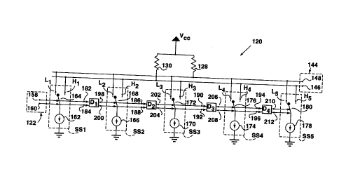
Reference is next made to Figure 5, which shows an improved cable
driver 120, according to the present invention.
The improved cable driver 120 comprises an input port 122, an
output port 144, two resistors 128 and 130 and five switching stages SSl,
SS2; SS3, SS4 and SS5 coupled in series by four delay stages, D1, D2, D3 and
D4.
Input port 122 comprises input terminals 158 and 160. Output port
144 comprises output terminals 146 and 148. Resistor 128, which has
resistance Rl2s, is coupled between V~~ and node 148 and resistor 130,
which has resistance Rlso~ is coupled between V~~ and node 146.
CA 02318934 2000-07-20
WO 99/38296
PCT/CA99/00031
-16-
Resistors 128 and 130 will be chosen to match the impedance of the
transmission line to which the improved cable driver 120 is coupled. This
eliminates the need for emitter follower output stages, so the associated
problems of ringing and overshoot are avoided.
Switching stage SSl comprises a current source 162 and a switch 164.
Current source 162 is coupled between switch 164 and ground. Switch 164
is responsive to a differential input signal Vin received at input port I22
and may couple current source 162 to node HI or to node Ll. Node H1 is
coupled to output terminal 148 and node L1 is coupled to output terminal
146.
Switching stages SS2, SS3, SS4 and SS5 each similarly comprise a
current source 166, 170, 174 or 178, respectively, and a switch 168, 172, 176
' or 180, respectively. These current sources and switches are coupled
together and coupled to ground and to output terminals 148 and 146 in the
same manner as current source 162 and switch 164.
Delay stage D1 is coupled to inp~.zf p~ri Iz2 at nodes 182 and 184 and
provides a delayed signal Vin-1 responsive to input signal Vin at nodes 198
and 200. Switch 168 is coupled to nodes 198 and 200 and is responsive to
signal Vin-i and may connect current source 166 to terminals H2 or L2.
Delay stages D2, D3 and D4 generate sequentially delayed signals Vin-2, Vin-3
and Vin-4 corresponding to Vin and Vin-1. They are similarly coupled
between switches 168 and 172, 172 and 176 and 176 and 180 respectively
such that each subsequent switch 172, 176 or 180 receives a signal
CA 02318934 2000-07-20
WO 99/38296
- I7-
PCT/CA99/00031
corresponding ~to differential input signal Vin-z~ Vin-3~ V;n-4 at a later
time
than the preceding switch.
As with the prior art cable driver 20, the improved cable driver 120
will typically be configured to produce a differential output signal Vout at
output terminals 146 and 148. The differential output terminal is defined
as the difference between the voltage at output terminal 148 (V14$) ~d ~e
voltage at output terminal 146 (V146)'
Vout - V148 V146
The improved cable driver operates as follows. A differential input
signal Vin is received at input terminals 158 and 160 and is directed to
switch 164. As with the prior art cable driver 20, the differential input
signal Vin is defined as the difference between the voltage received at
terminal 160 (Vl~) and the voltage received at terminal 158 (VlsB)'
Vin = V160 V158'
I5 Switch 164 is responsive to differential input signal Vin. If Vin is high
(i.e.
Vl6o > Vlss)~ switch 164 will couple current source 162 to node H1 and
conversely, if Vin is low (i.e. Vlbo < Vl5s), switch I64 will couple current
source 162 to node L1.
Delay stage D1 provides a delayed signal Vin-1 corresponding to
input signal Vin at nodes 198 and 200. Switch 168 is responsive to signal
Vin-1' ~ Vin-1 is high, switch 168 will couple current source 166 to node H2
CA 02318934 2000-07-20
-WO 99/38296
-18-
PCT/CA99/00031
and conversely, if Vin-1 is low, switch 168 will couple current source 166 to
node L2. In this manner, current sources 162 and 166 will be coupled to
the same output terminal 146 or 148.
Similarly switches 172, 176 and 180 are responsive to the delayed
signals provided by delay stages D2, D3 and D4, respectively, and will
couple current sources 170, 174 and 17$, respectively, to the same output
terminal 146 or 148 as current sources 162 and 166.
At steady state, if Vin is low, all five current sources 162, 166, 170, 174
and 178 will be coupled to output terminal 148. The voltage at terminal
148 (V148) will be
V148 ' VCC - R128(I162+I166+I170+I174+II78)'
The voltage at terminal 146 (V146) will be V~~, and the differential output
signal Vout will be
Vout ' V148 V146
' -~28(I162+I166+I170+I174+I178)
VOL
If Vin is high, all five current sources I62, 166, 170, 174 and 178 will be
coupled to output terminal 146 and the output voltage will be
Vout ' "130(I162+I166+I170+I174+I178)
= VaH
CA 02318934 2000-07-20
WO 99/38296
-19-
PCT/CA99/00031
Assuming that the differential input signal Vin is initially high,
differential output signal Vout will be equal to VoH. On the high to low
transition of Vin, switch 164 will switch current source 162 from terminal
Hl to L1. The voltage at terminal 146, will rise to
V146 - VCC Rl3o~I166+I170+I174+I178~
and the voltage at terminal I48 will fall to
V148 - VCC R128~I162~'
The differential output voltage Vout will fall to
Vout - V148 V146
to - -R128~I162~ + ~30~I166+I170+I174+I178~'
Delay stage DI will, after its configured delay period, produce a high
to low transition at terminals 198 and 200. Switch 168 will then switch
current source I2 from terminal H2 to terminal L2 and the differential
output voltage will fall to
1Jr Vout -' R128~I162+I166~ + Rl3o~Il~o+I1~4+I1~8~.
This process will continue until the delay periods of all four delay stages
Dl, D2, D3 and D4 have elapsed, all five switches 164, 168, 172, 176 and 180
have respectively coupled 162, 166, 170, 174 and 178 to output terminal 146
and Vout has fallen to VoL, as defined above.
20 Reference is next made to Figures 6A and 6B. Figure 6A shows the
transitions of switches 164, 168, 172, 176 and 180 from their respective H
nodes to their respective L nodes in response to a high to low transition of
CA 02318934 2000-07-20
WO 99/38296
-20-
PCT/CA99/00031
the differential input signal. Figure 6B shows the corresponding high to
low transition of Vout. Switches 164, I68, 172, 176 and 180 are non-ideal
switches with a finite transition time. The transition time of switches 164,
168, 172, 176 and 180 and the delay times of delay stages Dl, D2, D3 and D4
are preferentially chosen to ensure that the differential output signal Vout
is substantially linear. At the same time, the the 20% to 80% rise and fall
times of the differential output signal Vaut must exceed the specified
minimum time. As shown in Figures 6A and 6B, if the transition time of
the switching stages is too short, the output signal Vout will appear as a
staircase signal with each step being separated by the delay of the respective
delay stages D1, D2, D3 and D4.
Increasing the transition time of the switches 164, 168, 172, 176 and 180 will
provide a smooth transition, improving the linearity of differential output
signal Vaut. As shown in Figures 7A and 7B, which also shows the
transitions of switches 164, 168, 172, 176 and 180 and the differential output
signal Vo~t, the differential output signal Vout maY be made substantially
linear by making appropriate choices in the design of the switching stages
SSl, SS2, SS3, SS4 and SS5 and delay stages Dl, D2, D3 and D4. The design
of these elements is described in detail below. As an example, a
substantially linear differential output signal Vout may be achieved if the
delay time between the corresponding signals Vin, V~_i, Vin-2' Vin-s and
Vin-4 1S 70ps and the transition time of the switches 164, 168, 172, 176 and
CA 02318934 2000-07-20
~r=,n unw-rpa_M~)~~CHEn~ 02 :17- ;.'.- 0 : 17:35 : -~ +49 f~9 23994465:#15
- 1?-03-2000 CA 009900031
z~
180 is 150 ps. T'his will provide a differential autput signal with a
transition time of approximately 220 ps.
When a lover to high transition of V~ occurs subsequently, switches
164,16$,172, 176 and 180 ~nrill couple their respective current sources 162,
,5 166, 7.70,1.74 and 178 to output term 14$ and differential output signal
wilX retain to its ixiitial high output level V~H.
Since the high to low and low to high transitions of the differential
output signal Vast are substantially linear, the ratio of the 20% to 80% rise
time of Vout to the 2% settling tir3ne (i.e. the 98% rise time) will be
t~_~/t~ = 0.6/o.~s
= 0.612
= 61.2 %.
As described above, the ~0% to $0% rise time or fall time of the
dxffexential output signal Vout must exceed a minixnuxn time pexxod. xf
both the grior art cable driver 20 and the improved cable driver 120 are (1)
configured to operate with this auxtimuin 20% to 80°lo minimum
r~se/fall
time and (2) receive an input which mows them the meet the
requirement that the diffexential output signal out must settle to with 2%
of its steady state value (in order to reduce time fitter, as described
above),
2a the unproved cable dz~i~rer x20 will be capable of carrying a higher data
rate
than tine prior art cable dz~vex~ 20. The ratio of the ma~timum data rate
which may be carried by the improved cable driver 120 to the ~onaxznc~um
CA 02318934 2000-07-20
AMENDED SHEET
:rw vciv : F~~n -MUFNCH~:~~ U_> : 17- 3- 0 : 17 : 95 : -.~ +49 89 23994465 : #
16
17-03-2000
CA 009900031
_ 22
data rate W hick may be carried by the prior art cable driver 20 may be
calculated as follows:
612% / 35.4%
=1.73
- 5 Thus, the improved cable driver 12Q is capable of carrying a data rate
1.73
times higher than the prior art Cable driver 20, without increasing the
generation of electzomagneti~ radiation or increasing ~ Jitter in the
differential output signal 'V'~t. One skilled in the art will recognize that
if
the particular application in which improved cable driver 120 requires that
the fitter in the differential output sigzial ~r be less than 1.46%, as
calculated above, the benefit of the invention will be commensurately
greater.
Reference is next made to Figure $, which shows switching stage SS1
and delay stage D1 in detail. Switch 164 comprises a differential amplifier
x5 stage 220 and current source 162 comprises current mirror 222. Current
mirror 222 comprises transistor Q5, diode coru~eCted transistor Q6 and
reference current source 224, which are connected in the well latown
current mirror configuration. The bases of transistors Q5 and Q6 are
coupled together and the emitters o~ transistors Q5 and c~6 are connected to
a voltage source ~V'~e. The collector of transistor Q6 is coupled to VAC
through reference current source 224. The current drawn by transistor Q5
through differential amplifier stage 220 will depend on the current of
current source 224 in known manner. Differential amplifier stage 220
CA 02318934 2000-07-20 qMENDED SHEET
'WO 99/38296 PCT/CA99/00031
-23-
comprises two transistors Q3 and Q4, the emitters of which are connected
together. The base of transistor Q3 is coupled to input terminal 158 and the
base of transistor Q4 is coupled to input terminal 160. The collector of
transistor Q3 comprises node L1 and the collector of transistor Q4
comprises node H1. The emitters of transistors Q3 and Q4 are coupled to
the collector of transistor Q5.
The bases of transistors Q3 and Q4 are coupled to input terminals 158
and 160, respectively and receive the differential input signal across their
bases. One skilled in the art will be familiar with the operation of the
differential amplifier stage 220 and the current mirror 222 and will
understand the switching operation provided by the switching stage SSl.
Delay stage Dl is comprised of a differential amplifier consisting of
transistors Q7 and Q8, resistors 226 and 228 and a current mirror
comprising transistors Q9, diode connected transistor Q10 and reference
current source 230. The emitters of transistors Q7 and Q8 are connected
together and to the collector of transistor Q9. The base of transistor Q9 is
coupled the base of transistor Q10. The collector of transistor Q10 is couple
to V~~ through reference current source 230. The emitters of the
transistors Q9 and Q10 are connected to -VEE. The collectors of transistors
Q7 and Q8 are coupled to a voltage source VDD through resistors 226 and
228, respectively. Transistors Q7 and Q8 receive the differential input
signal Vin across their bases, which are connected to input terminals 160
CA 02318934 2000-07-20
k(w vnn~ : F4~A _~~yN~~~N 02 : 17- 3- 0 : 17 :36 : -» +49 89 2:3994450 : #17
1, 7-03-2000 CA 009900031
24
and 15$ respectively. The collectors of transistors Q7 and Q8 are coupled to
nodes 204 axed 198 respectively. One skilled in the art will understand that
the operation of Q7 and (~$ as a diffez~ential amplifier will produce signal
V~-1 at nodes 19$ and 200 (as discussed above) responsive to the
- 5 differential input signal V~, but delayed in time. The length of the delay
will depend on the current of current source Q9, which will depend on the
current of reference c~.uzent source 230 in laiown planner, the resistance of
resistors 226 and 228 and other characteristics of the bipolar technology in
which the cable driver circuit is realized. One skilled in the art will be
capable of selectixtg apptopxiate components to ensure that the transitions
of the differential output signal are substantially linear.
Although the invention has been described with reference to an
embodiment with 5 rise/fall time stages and 4 delay stages, the number of
rise/fall tame stages and delay stages may be varied to meet the operational
requirements of the particular context in which the improved cable driver
120 is used. One skilled in the art will be capable of modifyyng the
pzeferred e~onbodimex~t described here to meet such operational
requirements.
CA 02318934 2000-o~-ZO AMENDED SHEET