Note: Descriptions are shown in the official language in which they were submitted.
' '.1 ,' , W :,;. ~ ; : ' ;
A method for generation of electrical conducting or semiconducting
structures in three dimensions and methods for erasure of the same
structures.
The invention concerns a method for generating a combination of electrical
conducting and semiconducting structures in three dimensions in a composite
matrix, wherein the matrix comprises two or more materials provided in
spatially separate and homogenous material structures, wherein the materials
in response to the supply of energy can undergo specific physical and/or
chemical changes of state which cause transition from an electrical non-
conducting state to an electrical conducting and/or semiconducting state or
vice versa, or a change in the electrical conduction mode of the material,
wherein the material structures are generated in the form of thin layers by
combining two or more layers into a laminated multilayer structure which
constitutes the composite matrix with the combination of electrical
conducting and/or semiconducting structures in three dimensions, and
wherein the multilayer structure is generated by a successive deposition of
two or more layers into a stacked configuration on a carrier substrate; a
method for generating a combination of electrical conducting and/or
semiconducting structures in three dimensions in a composite matrix,
wherein the matrix comprises two or more materials provided in spatially
separate and homogenous material structures, wherein the materials in
response to the supply of energy can undergo specific physical and/or
chemical changes of state which cause transition from an electrical non-
conducting state to an electrical conducting and/or semiconducting state or
vice versa, or a change in the electrical conduction mode of the material,
wherein the material structures are generated in the form of thin layers by
combining two or more layers into a laminated multilayer structure which
constitutes the composite matrix with the combination of electrical
conducting and/or semiconducting structures in three dimensions, and
wherein the multilayer structure is generated by laminating two or more
self supporting layers into a stacked configuration; and a method for
generating a combination of electrical conducting and/or semiconducting
structures in three dimensions in a composite matrix, wherein the matrix
comprises two or more materials provided in spatially separate and
homogenous material structures and wherein the materials in response to the
supply of energy can undergo specific physical and/or chemical changes of
state which cause transition from an electrical non-conducting state to an
AMl;~ua~a s~r~~r
CA 02319428 2000-07-27
CA 02319428 2003-11-20
2
electrical conducting and/or semiconducting state or vice
versa, or a change in the electrical conduction mode of the
material, wherein the material structures are generated in
the form of thin layers by combining two or more layers
into a laminated multilayer structure which constitutes the
composite matrix with the combination of electrical
conducting and/or semiconducting structures in three
dimensions, and wherein the multilayer structure is
generated in a successive deposition of two or more layers
into a stacked configuration on a carrier substrate or by
laminating two or more self-supporting layers into a
stacked configuration. The invention also concerns a method
for erasing a combination of electrical conducting and/or
semiconducting structures generated in three dimensions in
a composite matrix, wherein the matrix comprises two or
more materials provided in spatially separate and
homogenous material structures, wherein the materials in
response to the supply of energy can undergo specific
physical and/or chemical changes of state which cause
transitions from an electrical non-conducting state to an
electrical conducting and/or semiconducting state or vice
versa or a change in the electrical conduction mode of the
material, wherein each material structure comprises a
generated pattern of substantially two-dimensional
electrical conducting and/or semiconducting structures
represented by a determined protocol, and wherein the
combination of electrical conducting and/or semiconducting
structures in three dimensions can be generated anew in the
matrix after erasure with the use of the method and
according to another determined protocol for two-
dimensional electrical conducting and/or semiconducting
CA 02319428 2003-11-20
2a
structures in each material structure; and a method for
erasing globally a combination of electrical conducting
and/or semiconducting structures generated in three
dimensions in a composite matrix, wherein the matrix
comprises two or more materials provided in spatially
separate and homogenous material structures, wherein the
materials in response to the supply of energy can undergo
physical and/or chemical changes of states which cause
transitions from an electrical non-conducting state to an
electrical conducting and/or semiconducting state and vice
versa or a change in the electrical conduction mode of the
material, and wherein the combination of electrical
conducting and/or semiconducting structure in three
dimensions can be generated anew in the matrix after
erasing by using the method and according to another
;, " ,w,3w; ~ . ; ,,., ,,
' ; ; ; ' ; , , ~ ..
determined protocol for two-dimensional electrical conducting and/or
semiconducting structures in each material structure.
More particularly the present invention concerns the fabrication of two- and
three-dimensional isolating, resistive, conducting and/or semiconducting
patterns and structures for use in electronic circuits which most particularly
consist of a single or several stacked layers of thin films.
The evolution of microelectronic technology shows a steady trend towards
smaller dimensions and reduced costs of the devices. Well-substantiated
predictions show that the performance is going to increase, while the price
per unit or device will decrease. However, today's microelectronic
technology is substantially based on crystalline silicon and shows an
increasing tendency towards diminishing returns, mainly due to the inherent
limitations associated with the complexity of ultra-high resolution
lithography and increasing demands of the material processing.
Extrapolations of the present technologies based on crystalline silicon may
hence not be expected to offer dramatic breakthroughs in regard of either
performance or price and future improvements shall require manufacturing
plants and manufacturing equipment which are extremely capital-intensive.
Microelectronics based on thin-film technology may on the other hand
confidently be predicted to deliver in the near future products representing
real breakthroughs in regard of performance as well as of price. The shift
from crystalline inorganic semiconductors to microcrystalline, polycrystalline
or amorphous inorganic or organic semiconductors will introduce entirely
novel boundary conditions with regard to the production of microelectronics
;..
'- 25 and particularly by the blanks having form factors which make large
areas
possible, i.e. the substrates may be large sheets instead of wafers cut from
blanks of limited size, and great flexibility v~ith regard to architectures,
something which will be essential factors in the expected development of
tomorrow's electronic technology. In the present invention special emphasis
will be placed on the use of organic materials due to the ease whereby they
may be processed with basis in the use of Large areas and multilayer blanks
with precisely controllable thickness, as well as their vast potential for
chemical tailoring of the desired material properties.
Particularly before the use of electronics based on amorphous materials can
fulfil their expected potential, further developments in certain areas are
All=NDED SH~fT
CA 02319428 2000-07-27
:, .; ,~~ 4~..;
. , , . . , . , ,
,... , . ,
'" , " . ,
required. In the recent years an effort has been made to (improve the
semiconducting properties of organic semiconducting thin-film materials,
which have given dramatic and rapid increase in the transistor performance
up to a point where organic-based transistors may now compete with
transistors based on amorphous silicon (see for instance Y.-Y. Lin,
D.J. Gundlach, S.F. Nelson and T.N. Jackson, "Pentacene-Based Organic
Thin Film Transistors", IEEE Transactions on Electron Devices, August
1997). Other on-going projects will lead to coating processes for thin film in
order to generate organic and amorphous silicon semiconductors at low
temperatures and with compatibility with a broad range of organic and
inorganic substrate materials. This has lead to the development of extremely
cheap electronic devices with large areas based on the use of high-volume
manufacturing methods.
In spite of this development a wholly satisfactory solution to how the
fabrication technology shall be adapted and made suitable for a low-cost
flexible high-volume production of electrical connections in the thin-film
structures forming the electronic circuits is still lacking. Currently thin-
film
devices are based on amorphous silicon manufactured with current paths and
conductors patterned with traditional methods such as lithography and
vacuum metallization. The latter method has formerly also been applied to
circuits for demonstration of organic-based semiconductor thin-film devices
(see for instance A.R. Brown & a1. "Logic gates made from polymer
transistors and their use of ring oscillators", Science 270: 972-974 (1995)).
Alternatively, screen printing with conducting "ink" has been used to make
transistors on flexible polymer substrates (see for instance F. Garnier & al.,
- "All-polymer field-effect transistor realized by printing techniques",
Science
265:1884-1886 (1994)). Even though lithography may provide high
resolution, it is relatively complex and includes typically wet chemistry
steps
which are undesirable in high-volume production of multilayer organic
thin-film structures. Screen printing with ink is also far from ideal, as it
only
provides low to moderate resolution besides being a "wet" method.
As examples of prior art such it is evident from available patent literature
may also be mentioned US patent No. 5 043 251 (Sonnenschein & al.) which
discloses a process for three-dimensional lithography of amorphous polymers
for generating a momentary permanent pattern in a polymer material and
which comprises steps for providing doped non-crystalline layers or films of
Al~ict~~;~~ ~tET
CA 02319428 2000-07-27
,:
' ; ; "; ' ; ; ; ;
a polymer in a stable amorphous state under humane operating, conditions. In
manufacturing the patterns the film is masked optically and is exposed
through the mask to radiation with sufficient intensity to cause ablation of
the exposed portions such that a distinct three-dimensional imprint is
S generated in the film. This process has among other been proposed for use in
the manufacture of an optical data storage disk. Further it is from US patent
No. 5 378 916 (Mantell) known a photo-sensitive device in the form of a
single-crystal structure, wherein different portions of the structure rnay
have
different compositions. Particular the structure forms a two-dimensional
array and a first photosensitive portion comprises a material which generates
electron-hole pairs when it is exposed to light within a predetermined first
wavelength range, while another photosensitive portion comprises a material
which is adapted to generate electron-hole pairs when it is exposed to light
within another wavelength range distinctively different from the first
wavelength range. Yet further there is from US patent 5 677 04I (Smayling)
known a transistor device which is made by forming a doped layer of
radiation-sensitive material on a substrate. The radiation-sensitive material
may among others be polyimide, polymer, an organic dielectric, a conductor
or a semiconductor. The substrate may be silicon, quarts, gallium arsenide,
glass, ceramic, metal or polyamid. A neutral or undoped layer of another
radiation sensitive material is formed over the doped layer. First and second
source/drain areas are then formed in the neutral layer and extend down to a
top portion of the doped layer. A gate area is formed in the top portion of
the
neutral layer between the first source/drain area and the second source/drain
area such that a channel area in the doped layer is provided under the gate
t area. Drain/source and gate electrodes as formed by irradiation of the
uppermost neutral layer through a mask patterned in accordance with the
desired electrode pattern and realized such that it intensity-modulates the
radiation. In addition the mask may also be realized as a phase-shifting mask.
Finally it is from the article "Polymeric integrated circuits and light-
emitting
diodes" of D.M. de Leeuw & al., IEDM, pp. 331-336 (1997) known a
MISFET wholly realized in polymer and with the use of polymer materials
which are given the desired electrical properties by an exposure to UV
radiation. In the manufacture photochemical patterning of doped electrical
conducting polyaniline films, so-called PANI thin films is used. The films
are dissolved in a suitable solution, whereafter a photo-initiator is added to
the solution which has been deposited on a suitable substrate such as a
E~I~iciv~~~ S~~IrT
CA 02319428 2000-07-27
' ; ; ' ;' ~ , , ,
polyimide film. By thereai'ter exposing the PANI film to deep UV radiation
through a mask the initially conducting polyaniline is converted in the
exposed areas to the non-conducting leucoerneraldine form. The starting
point here is accordingly a conducting polymer material, the area resistance
S of which initially is 1 kiloohm/square, but which after the exposure obtains
an area resistance of more than 1013 ohm/square. In this manner dielectric
structures may be generated in an otherwise conducting matrix. Fig. 1 shows
a MISFET according to Leeuw & al. comprising a polyimide substrate 1 with
a PANI thin film which after exposure to UV light through suitable masks
forms isolating structures 6 in the otherwise conducting thin-film material 3.
The still conducting areas 3 in the PANI film define respectively the source
and drain electrode of a MISFET transistor. Above the PANI film a further
layer 4 is deposited in the form of a thin film of polythienylenevinylene or
PTV which is an organic semiconductor material. This layer 4 substantially
determines the electrical parameter of the MISFET transistor. A film 5 of
polyvinyl phenol PVP which forms the gate isolator of the transistor and is
opaque to UV radiation and visible light is deposited over the PTV film 4.
Another PANI film is again deposited on the top of the PTV film 5 and
patterned by radiation with UV light such that isolating structures 6 are
formed. A still electrical conducting area 2 fonns the gate electrode of the
MISFET structure.
If several transistors of this kind as mentioned above shall be combined in
integrated circuits realized in the form of stacked film Layers, vertical
current
paths between for instance source and drain electrodes in a transistor and the
gate electrode in another transistor must be used. Such vertical current paths
may in principle be realized mechanically, for instance by depositing a metal
film over vertically etched steps in the structure. Otherwise a close analogy
is
the use of throughplated holes in circuit boards to realize a vertical
connection between current paths on the upper and lower side of the circuit
board.
The main object of the present invention is to provide improved fabrication
methods for conducting connections and electrodes in microelectronic
components and particularly microelectronic devices with large areas on
flexible substrates by means of processes which combine high-volume
fabrication at low costs. Particularly, it is an object of the invention to
provide such fabrication methods that they may be used on layered physical
A~f~NDI_~ SHEET
CA 02319428 2000-07-27
CA 02319428 2003-11-20
7
devices, for instance in the form of a large number of
adjacent stacked thin-film layers, thus generating three-
dimensional circuit structures. The present invention will
thereby make possible flexible and cheap, but
simultaneously also singularly simple and precise
fabrication of devices such as flat display devices, logic
circuits, memory devices, etc.
Further it is also an object of the invention to provide
methods for erasing such three-dimensional circuit
structures in situ, such that the material in the
structures is converted back to an initial virgin state
whereafter it anew may be reconfigured in the form of
electrical conducting and semiconducting structures in
three dimensions, but for instance with another pattern or
another structure than the original.
The above-mentioned features and advantages are according
to a first aspect of the present invention realized with a
method characterized by generating a combination of two-
dimensional electrical conducting and semiconducting
structures in a layer immediately after the deposition of
the layer on the substrate or an adjacent layer and before
depositing a further layer on the first-mentioned layer, by
irradiating each layer with a radiation of a given
intensity or frequency characteristic adapted to the
specific response of the material to the energy supplied by
the radiation, modulating the radiation spatially in each
case according to a determined protocol which represents a
predetermined pattern of electrical conducting and
semiconducting structures in the relevant layer, whereby in
response to the energy supplied with the radiation the
CA 02319428 2003-11-20
8
combination of two-dimensional electrical conducting and
semiconducting structures is generated in the layer with
the pattern predetermined by the protocol, such that the
composite matrix formed by separate adjacent layers with
the combination of two-dimensional electrical conducting
and semiconducting structures is provided with the
combination of electrical conducting and semiconducting
structures in three dimensions.
Preferably, according to the first aspect of the invention
it is advantageous selecting electromagnetic radiation used
for the irradiation among one or more of the spectral
ranges gamma, x-ray, ultraviolet, visible light, infrared
and microwave, or selecting particle radiation used for the
irradiation among one or more of the following types of
particles, viz. elementary particles including protons,
neutrons or electrons; ions, molecules or material
aggregates.
Preferably, further it is according to the first aspect of
the invention advantageous modulating the radiation
spatially in a plane substantially parallel with a layer,
by means of a mask which is patterned according to the
determined protocol, the mask modulating intensity and/or
phase of the radiation incident thereto for generating the
combination of electrical and semiconducting structures in
the layer, or modulating the radiation spatially in a plane
substantially parallel with the layer by concentrating the
radiation into a beam with dimensions compatible with the
dimensions of the electrical conducting and semiconducting
structures and scanning the layer with the beam which is
intensity-modulated according to the determined protocol
CA 02319428 2003-11-20
9
for generating the combination of two-dimensional
electrical conducting and semiconducting structures in the
layer.
Preferably, according to the first aspect of the invention
it is advantageous generating one or more two-dimensional
electrical conducting and semiconducting structures in a
layer, such said structure or structures according to the
protocol register with one or more two-dimensional
electrical conducting and/or semiconducting structures
generated in an adjacent, already deposited layer, whereby
one or more vertical electrical conducting and/or
semiconducting channels are generated in the cross-
direction through the layers.
The above-mentioned features and advantages are according
to a second aspect of the present invention realized with a
method characterized by generating the combination of two-
dimensional electrical conducting and/or semiconducting
structures in a layer before the layer is laminated to an
adjacent layer, irradiating each layer with a radiation of
a given intensity or frequency characteristic adapted to
the specific response of the material to the energy
supplied by the radiation, modulating the radiation
spatially in each case according to a determined protocol
which represents a predetermined pattern of electrical
conducting and/or semiconducting structures in the layer,
whereby in response to the energy supplied with the
radiation the combination of two-dimensional electrical
conducting and/or semiconducting structures is generated in
the layer with the pattern predetermined by the protocol,
such that the composite matrix formed by laminating
CA 02319428 2003-11-20
together separate layers with two-dimensional electrical
conducting and/or semiconducting structures is provided
with the combination of electrical conducting and/or
semiconducting structures in three dimensions.
Preferably, according to the second aspect of the invention
it is advantageous selecting electromagnetic radiation used
for the irradiation among one or more of the spectral
ranges gamma, x-ray, ultraviolet, visible light, infrared
and microwave, or selecting particle radiation used for the
10 irradiation among one or more of the following types of
particles, viz. elementary particles including protons,
neutrons or electrons; ions, molecules or material
aggregates.
Preferably, further it is according to the second aspect of
the invention advantageous modulating the radiation
spatially in a plane substantially parallel with a layer,
by means of a mask which is patterned according to the
determined protocol, the mask modulating intensity and/or
phase of the radiation incident thereto for generating the
combination of electrical and/or semiconducting structures
in the layer, or modulating the radiation spatially in a
plane substantially parallel with the layer by
concentrating the radiation into a beam with dimensions
compatible with the dimensions of the electrical conducting
and/or semiconducting structures and scanning the layer
with the beam which is intensity-modulated according to the
determined protocol for generating the combination of two-
dimensional electrical conducting and/or semiconducting
structures in the layer.
CA 02319428 2003-11-20
11
Preferably, according to the second aspect of the invention
it is advantageous positioning the layer in the lamination
to an adjacent layer such that one or more two-dimensional
conducting and/or semiconducting structures in the first
mentioned layer according to the protocol register with one
or more two-dimensional electrical conducting and/or
semiconducting structures in adjacent layers, whereby one
or more vertical electrical conducting and/or semi
conducting channels are generated in the cross-direction
through the layers.
Finally, the above-mentioned features and advantages are
according to a third aspect of the present invention
realized with a method characterized by generating a
combination of two-dimensional electrical conducting and/or
semiconducting structures in a layer after the deposition
of all layers into a stacked configuration on a substrate
or after the lamination of all layers into the stacked
configuration has taken place by irradiating one or more,
but not all layers in the stacked configuration selectively
in order to generate electrical conducting and/or
semiconducting structures in the relevant selected layer or
layers without causing a response in the non-selected
layers, each layer being irradiated with a radiation of a
given intensity or frequency characteristic adapted to the
specific response of the material to the energy supplied by
the radiation, and modulating the radiation spatially in
each case according to a determined protocol which
represents a predetermined pattern of electrical conducting
and/or semiconducting structures in the relevant layer,
whereby in response to the energy supplied with the
radiation two-dimensional electrical conducting and/or
CA 02319428 2003-11-20
12
semiconducting structures are generated in the layer with
the pattern predetermined by the protocol, such that the
composite matrix formed by the stack of separate adjacent
layers with two-dimensional electrical conducting and/or
semiconducting structures is provided with electrical
conducting and/or semiconducting structures in three
dimensions.
Preferably, according to the third aspect of the invention
it is advantageous selecting electromagnetic radiation used
for the irradiation among one or more of the spectral
ranges gamma, x-ray, ultraviolet, visible light, infrared
and microwave, or selecting particle radiation used for the
irradiation among one or more of the following types of
particles, viz. elementary particles including protons,
neutrons or electrons; ions, molecules or material
aggregates.
Preferably, further it is according to the third aspect of
the invention advantageous modulating the radiation
spatially in a plane substantially parallel with a layer,
by means of a mask which is patterned according to the
determined protocol, the mask modulating intensity and/or
phase of the radiation incident thereto for generating the
combination of electrical and/or semiconducting structures
in the layer, or modulating the radiation spatially in a
plane substantially parallel with the layer by
concentrating the radiation into a beam with dimensions
compatible with the dimensions of the electrical conducting
and/or semiconducting structures and scanning the layer
with the beam which is intensity-modulated according to the
determined protocol for generating the combination of two-
CA 02319428 2003-11-20
13
dimensional electrical conducting and/or semiconducting
structures in the layer.
Preferably, according to the third aspect of the invention
it is advantageous selecting one or more layers for
generating electrical conducting and/or semiconducting
structures by irradiating the selected layer or layers with
radiation of specific radiation characteristics or a given
power, the selected layer or layers being formed of a
material which responds to one or more of the radiation
characteristics and/or the power, or combinations thereof.
Preferably, it is according to the third aspect of the
invention preferred that the specific radiation
characteristics are intensity and/or frequency; one or more
layers for generating electrical conducting and/or
semiconducting structure preferably being selected by
irradiation with electromagnetic radiation on two or more
frequencies or within two or more wavelength bands, such
that the irradiation on a given frequency or in a given
wavelength band causes a response in one or more, but not
all layers.
Preferably, it is according to the third aspect of the
invention also advantageous adding beforehand one or more
additives which have a spectral absorption on a given
frequency or in a given wavelength band, to the material in
one or more layers in order to cause the response to the
radiation on a given frequency or in a given wavelength
band, at least two layers in the stacked configuration
thereby obtaining mutually different absorption spectra,
and then also generating the electrical conducting and/or
CA 02319428 2003-11-20
13a
semiconducting structure in a layer by the radiation
absorption in the additive or additives in the layer
forming reaction centres which cause a change in the
electrical conductivity or conduction mode of the layer
material, or generating the electrical conducting and/or
semiconducting structures in a layer by the radiation
absorption in the additive or additives causing a heating
with subsequent changes in the electrical conductivity or
conduction mode of the heated layer material.
Preferably, according to the third aspect of the invention
the electrical conducting and/or semiconducting structures
in two or more layers are advantageously generated in
positions where one or more electrical conducting and/or
semiconducting structures according to the protocol
respectively form one or more vertical electrical
conducting and/or semiconducting channels in the cross-
direction through the layers in the stacked configuration,
and then preferably providing according to the protocol the
electrical conducting and/or semiconducting structure which
forms or form a vertical channel through the layer
according in electrical conducting and/or serniconducting
connection with one or more two-dimensional electrical
conducting and/or semiconducting structures in this layer.
Preferably each channel is formed with a conductivity or
conduction mode which is constant between the layers or
with a conductivity or conduction mode which varies between
the layers.
Further the above-mentioned features and advantages are
realized according to the present invention with a method
for erasing which is characterized by irradiating each
CA 02319428 2003-11-20
13b
material structure with radiation of a given intensity
and/or frequency characteristic adapted to the specific
response of the material to the energy supplied by the
radiation, and by modulating the radiation spatially in
each case according to the protocol which represents the
generated pattern of electrical conducting and/or
semiconducting structures in the relevant material
structure, whereby the two-dimensional electrical
conducting and/or semiconducting structures present in the
material structures in response to the energy supplied by
the irradiation are erased according to the protocol, such
that the material of the material structure thereafter in
its entirety arrives in the electrical non-conducting
state.
Preferably, in the method for erasing it is advantageous
selecting the electromagnetic radiation used for the
irradiation among one or more of the spectral ranges gamma,
x-ray, ultraviolet visible light, infrared and microwave;
or selecting particle radiation used for the irradiation
among one or more of following particles, viz. elementary
particles including protons, neutrons and electrons; ions,
molecules and material aggregates.
Preferably, further it is in the method for erasing
according to the invention advantageous modulating the
radiation spatially in a plane substantially parallel with
a material structure by means of a mask which is patterned
according to the determined protocol, the mask modulating
intensity and/or phase of the radiation incident thereto
for erasing the electrical conducting and/or semiconducting
structures in the material structure; or modulating the
CA 02319428 2003-11-20
13c
radiation spatially in a plane substantially parallel with
the material structure by concentrating the radiation into
a beam with dimensions compatible with the dimensions of
the electrical conducting and/or semiconducting structures,
and scanning the material structure with the beam which is
intensity-modulated according to the determined protocol
for erasing of electrical conducting and/or semiconducting
structures in the material structure.
Preferably, wherein the material structures in the matrix
are formed by thin layers in stacked configuration, it is
in the method for erasing advantageous irradiating one or
more, but not all layers in the stacked configuration
selectively for erasing electrical conducting and/or
semiconducting structure in the selected relevant layer or
layers without causing a response in the non-selected
layers, and then preferably selecting one or more layers
for erasing of electrical conducting and/or semiconducting
structure by irradiating the selected layer or layers with
specific radiation characteristics or a given power, the
selected layer or layers being formed of a material which
responds to one or more of the radiation characteristics
and/or the power or combinations thereof.
Finally the above-mentioned features and advantages
according to the present invention is also realized with a
method for global erasing which is characterized by
irradiating the matrix globally with radiation with a given
intensity and/or frequency characteristic adapted to the
specific response of the material to the energy supplied by
the radiation until the material in the matrix in response
CA 02319428 2003-11-20
13d
to the energy supplied by the irradiation in its entirety
arrives in the electrical non-conducting state.
Preferably, according to the invention it is in that
connection advantageous selecting electromagnetic radiation
used for the irradiation among one or more of the spectral
ranges gamma, x-ray, ultraviolet, visible light, infrared
and microwave or selecting particle radiation used for the
irradiation among one or more of the following particle
types, viz. elementary particles including protons,
neutrons and electrons; ions, molecules and material
aggregates.
According to the present invention, there is also provided a
method for generating electrically conducting, semiconducting,
and non-conducting structures in three dimensions in a
composite matrix comprising:
irradiating each material structure with a radiation
of a given intensity or frequency characteristic adapted to
the specific response of the material to energy supplied by
the radiation, wherein the matrix comprises two or more of
said materials provided in spatially separate and
homogenous material structures and wherein the materials in
response to the supply of energy can undergo specific
physical and/or chemical changes of state which cause
transition from an electrically non-conducting state to an
electrically conducting and/or semiconducting state or vice
versa, or a change in the electrically conduction mode of
the material; and
CA 02319428 2003-11-20
13e
modulating the radiation spatially in each case
according to a determined protocol which represents a
predetermined pattern of electrically conducting and/or
semiconducting structures in the relevant material
structure, whereby in response to the energy supplied with
the radiation two-dimensional electrically conducting and
semiconducting structures are generated in the material
structure with the pattern predetermined by the protocol,
such that the composite matrix formed by laminating
separate adjacent material structures with two-dimensional
electrical conducting and semiconducting structures is
provided with electrically conducting and semiconducting
structures in three dimensions.
According to the present invention, there is also provided a
method for erasing electrically conducting, semiconducting,
and non-conducting structures generated in three dimensions
in a composite matrix comprising:
irradiating each material structure with radiation of
a given intensity and/or frequency characteristic adapted
to the specific response of the material to energy supplied
by the radiation, wherein the matrix comprises two or more
materials provided in spatially separated and homogenous
material structures, wherein the materials in response to
the supply of energy can undergo specific physical and/or
chemical changes of state which cause transitions from an
electrically non-conducting state to an electrically
conducting and semiconducting state or vice versa or a
change in the electrically conduction mode of the material,
and wherein each material structure comprises a generated
pattern of substantially two-dimensional electrically
CA 02319428 2003-11-20
13f
conducting and semiconducting structures represented by a
determined protocol; and
modulating the radiation spatially in each case
according to the protocol which represents the generated
pattern of electrically conducting and semiconducting
structures in the relevant material structure, whereby the
two-dimensional electrically conducting and semiconducting
structures present in the material structures in response
to the energy supplied by the irradiation are erased
according to the protocol, such that the material of the
material structure is transformed to the electrically non-
conducting state and wherein electrically conducting and/or
semiconducting structures in three dimensions can be
generated anew in the matrix after erasure.
According to the present invention, there is also provided
a method for erasing globally electrically conducting,
semiconducting, and non-conducting structures generated in
three dimensions in a composite matrix comprising:
irradiating the matrix globally with radiation of a
given intensity and/or frequency characteristic adapted to
the specific response of a material to the energy supplied
by the radiation until the material in the matrix in
response to energy supplied by the irradiation in its
entirety is transformed to the electrically non-conducting
state, wherein the matrix comprises two or more materials
provided in spatially separate and homogenous material
structures, wherein the materials in response to the supply
of energy can undergo physical and/or chemical changes of
states which cause transitions from an electrically non-
CA 02319428 2003-11-20
13g
conducting state to an electrically conducting and
semiconducting state or vice versa or a change in the
electrically conduction mode of the material, wherein
electrically conducting and semiconducting structure in
three dimensions can be generated anew in the matrix after
erasing by using the method as stated in any of the claims
1-5 and 12-22 and according to another determined protocol
for two-dimensional electrically conducting and
semiconducting structures in each material structure.
According to the present invention, there is also provided
a method for generating three dimensional electrical
structures in a composite matrix, the electrical structures
exhibiting both electrically conducting, semiconducting,
and non-conducting characteristics, the composite matrix
including two or more spatially separate and homogenous
material structures associated with two or more materials,
the method comprising:
irradiating each of the two or more material
structures with a radiation of a predetermined
characteristic, the predetermined characteristic adapted to
each of the two or more materials such that the specific
response of the two or more materials to the predetermined
characteristic causes specific changes of state resulting
in one or more transitions from an electrically non-
conducting state to an electrically conducting and
semiconducting state, or an electrically conducting and
semiconducting state to an electrically non-conducting
state, or a first electrical conduction mode to a second
electrical conduction mode;
CA 02319428 2003-11-20
13h
modulating the radiation spatially according to a
predetermined protocol to form a predetermined pattern
associated with the electrically conducting and
semiconducting structures; and
wherein in response to the radiation two dimensional
electrically conducting and semiconducting structures are
generated in the two or more materials according to the
predetermined pattern such that the composite matrix formed
by laminating the two or more materials is provided with
electrically conducting and semiconducting structures in
three dimensions.
The invention shall now be explained in more detail in
connection with a survey of its basic principles and with
use of exemplary embodiments in connection with the
appended drawings, wherein:
fig. 1 shows a MISFET with electrodes formed of a
photoconvertible material according to prior art,
figs. 2a, b, c schematically steps in the method for
generating according to the present invention,
.; w'.1'4': ,", ; ,". ,".
', ' , '~.' '~ '«' '
fig. 3 schematically the joining of self supporting layer into a multilayered
structure,
fig. 4a schematically another embodiment of the method for generating
according to the invention,
fig. 4b schematically the spectral responses of photoconvertible materials
used in the embodiment in fig. 4a,
fig. 5 a schematic section through a laminated multilayer structure which
comprises conducting or semiconducting structures generated by the method
according to the present invention,
fig. 6 a schematic section through a diode structure generated by the method
according to the present invention,
[_
fig. 7 a schematic section through a MOSFET structure generated by the
method according to the present invention,
fig. 8 a schematic section through a logic inverter structure based on the
MOSFET structure in fig. 7 and generated by the method according to the
present invention,
fig. 9 the equivalent diagram of an AND gate realized in CMOS technology,
figs. l0a-d in plan view sublayers in an AND gate structure generated by the
method according to the invention and according to the equivalent diagram in
fig. 8 with the use of MOSFET structures as shown in fig. 7,
fig. 11 the AND gate structure in fig. 10 as a stacked multilayer
a
configuration, but exploded in sublayers,
fig. 12 schematically another variant of the AND gate structure in fig. 10 and
with the separate CMOS structures provided mutually connected in a vertical
configuration,
fig. 13 a schematic production line for multilayer circuits on a substrate and
using the method for generating according to the present invention, and
fig. 14 schematically the spectral response of photoconvertible materials as
used in the embodiment in fig. 13.
AIVPENpE~ ,~~~-~-
CA 02319428 2000-07-27
, I ,. I
1 1
1 i n ~ w I I ~ I r . v
n n o 1 I p I I 1 I n V f 1 n I I
r I n I r I I I 1 I I ,
Now the basic principles of methods according to the present invention
whereby three-dimensional structures with a well-defined mode and degree
of electrical conduction are generated by spatially controlled patterning in
situ in convertible materials which have such properties that their electronic
properties are converted reversibly or irreversibly, under the effect of
radiation, heat or electrical f elds. The methods for generating such
structures
according to the present invention is based on the use of irradiation, either
with electromagnetic radiation or particle radiation, and in practice this
implies that also when the conversion takes place due to heating effects, heat
which arises in the material due to irradiation is used. Initially the
three-dimensional electrical conducting or semiconducting structures can be
generated as two-dimensional structures of this kind by direct local influence
of the radiation on a single layer and appears as three-dimensional by joining
single layers into a multilayer structure. Indirectly the electrical
conductive
or semiconductive structures may be generated by additives which, when
stimulated by the irradiation, influence the convertible material such that
its
electronic properties are changed. In case of homogenous convertible
materials the radiation influence must be spatially defined in a corresponding
three-dimensional pattern. Even though the invention in principle includes
homogenous materials, the explanation of the method in the following
essentially will be directed towards multilayer structures or layered
structures
where the three-dimensional definition of the electrical conducting or
semiconducting structures is obtained by a different responsitivity to the
radiation effect in two or more layers of convertible material which form a
stack. Typically the convertible material will be an organic material, for
instance a molecule, an oligomer or a polymer where a phase transition from
an initial first state to a new second state takes place upon irradiating, for
instance with light in a given wavelength band. As mentioned in the
following, if is presupposed that the most important change taking place from
the first to the second state, is the degree of electrical conduction. In the
following the methods for generating and erasing of electrical conducting or
semiconducting structures will be exemplified by spatially controlled
irradiation of layered or layerwise built-up irradiation convertible materials
(ICM).
For polymers such as polyaniline it is as shown in the above-mentioned paper
by de Leeuw & al., observed conduction ratios between two states as high as
101°. In this case it concerned in situ conversion of a single layer of
AMENDED SHE
CA 02319428 2000-07-27
16~~
irradiation convertible material from conducting to non-conducting state in
order to generate electrical connections in a single electronic circuit.
Electrical conducting connections in doped polyaniline films (PANI films)
were defined by exposure to deep UV radiation through a patterned mask.
A multilayer stack of different irradiation convertible materials may be
provided on a substrate which may be flexible or rigid, conducting or
non-conducting and the radiation convertible material be made conducting,
semi-conducting or isolating in desired patterns by using one of the following
procedures, viz. either patterned irradiation of a number of single layer
irradiation convertible materials and sequential or simultaneous combination
of the layers into a multilayer stack, or by using patterned irradiation of a
preformed multilayer stack of irradiation convertible materials ICM, different
types of irradiation with different radiation characteristics being used such
that the radiation interacts selectively with one or more designated layers in
the stack. Multilayer stacks of irradiation convertible material are of
particular interest in connection with multilayer thin-film circuits where it
is
required to generate electrical conducting lines, current paths, connection
points or electrodes in several layers such that the conducting structures in
one layer has a precisely controlled spatial relationship to the conducting
structures in the layers which are located above or below. One example is
thin-film field effect transistors (TFET) where the source and drain electrode
in a layer must be correctly positioned relative to the gate electrode and
with
intervening isolating and semiconducting layers. Another example is
electrical connections between the layers where traditional solutions in many
cases are unsatisfactory, for instance by incorporating a number of steps such
as forming open channels or vias between suitable points which then shall be
electrically connected in the different layers and with subsequent filling or
casing of the channels with a conducting material, such as this finds its
parallel in the use of through-plated holes in circuit boards to obtain a
connection from the front to the back of the circuit board. A third instance
is
the generation of capacitors by defining conducting areas which are aligned
mutually opposite in two layers separated by an isolating layer. Evidently not
only highly conducting, but also isolating resistive and semiconducting
patterns in multilayer structures are of the greatest importance. Such as will
be explained in more detail in the following, patterns of this kind may be
generated by using the method for generating electrical conducting or
semiconducting structures or patterns according to the present invention.
A~VIENDED S
CA 02319428 2000-07-27
" i~:; ,. , ,,. ,.,
,:
: . .
, , , , , , .
. " . ~ , . ~ ,
, . , , ~ ~ ,; ..
, " . .,
With regard to the precision and clarity the following description shall,
however, be introduced by emphasizing on how patterns and
three-dimensional structures which either are very good or very bad electrical
conductors shall be defined.
Multilayer structures as described herein are of particular interest when they
are integrated with thin-film semiconductors in order to form complete
circuits. The present standard procedures for fabricating microelectronic
circuits which exploit the semiconducting properties of a common silicon
substrate restrict automatically the realizable architectures to the kind
which
allows access to the substrate for all active devices. If the method according
to the present invention is used for generating electrical conducting or
semiconducting structures in three dimensions by means of stacked layers,
whole devices may be generated in this manner without any essential
restriction with regard to the size or complexity as scaling quite simply
takes
place by joining more layers to the stack. As each layer may be made thin, for
instance with an order of magnitude of 10-100 nm, the resulting volumetric
density for the circuit patterns and hence the performance per weight or
volume unit may be extremely high. Further hybrid architectures may be
realized with the use of layers which includes irradiation-converted
electronic structures which are formed on the top of and function in
cooperation with additional silicon-based electronic circuits.
The basic object of the present invention is the generation of electrical
conducting, semiconducting or resistive structures in three-dimensions in a
multilayer material in a monolithic format and may be realized using a
2~ number of different fabrication procedures. Such procedures will be
described separately in the following. The first step is a patterned
conversion
of a single-layer irradiation-convertible material ICM with subsequent
sequential combination of the layers into a multilayer stack. Multilayer
structures may be formed in the irradiation convertible materials which are
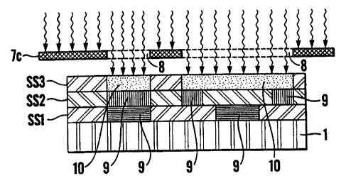
deposited and processed sequentially as a set of thin film layers SS l, SS2,
SS3 on a common substrate l, such this is shown in figs. 2a, b, c. The
substrate 1 may be a rigid or flexible sheet with arbitrary thickness or it
may
be a continuous tape in a reel-to-reel process. In case of irradiation
convertible materials ICM the sequential process takes place as follows. A
first coating layer SSl is applied to the substrate followed by a spatially
controlled irradiation which forms conducting structures 9. The irradiation
AMENDED SHED
CA 02319428 2000-07-27
. n n s . ~ . . . i ~ . .
_. i , , . ~ ~ ~ ~ . . .
i ~ . , ~ ~ ,
. , n ~ . ~ . . ,
a , . , n , . , r ~ .
i
n . n n
takes place through a first mask or spatial light modulator (SLM) 7a.
Depending on predetermined process conditions the irradiation will cause the
direct conversion into another conduction state or generate a latent image
which may be developed in a post-irradiation process. The last process step
may be exposure to suitable chemical species in liquid or gaseous state and
may in some cases also be stimulated by global irradiation. An example of
direct photoconversion from conducting to a substantially non-conducting
state without a process step after irradiation, is the use of deep UV
irradiation with polyaniline as mentioned above with reference to the paper
by de Leeuw & al. An example of photoconversion from conducting to a
substantially non-conducting state with the use of wet chemistry is the
exposure of anthraquinone-2-sulphinic acid-(AQSA)-doped polypyrrol to
blue or ultraviolet light, followed by wet processing.
After the processing of the first layer SS1, a second layer SS2 is applied on
the top of the first, for instance by evaporation, sputtering, application of
a
liquid (for instance by spin or dip coating), doctor blading or by lamination
of a thin film onto the first layer SS1. The photoconversion of the second
layer SS2 takes place by means of spatially controlled irradiation and for
instance conducting structures 9 are generated through the mask or SLM 7b.
If the photoconversion takes place directly, i.e. is effected by means of
irradiation alone, measures must be taken to prevent activation of the
underlying layer SS 1. This may for instance take place by incorporating a
radiation shielding layer between the two layers SS1, SS2, as the
radiation-shielding layer may be a spectral filter or absorbing or reflecting
media, or by using coating layers with different spectral photosensitivities.
If
the photoconversion makes use of a photoprocessing after the irradiation,
measures must be taken to prevent that chemical reactants penetrate to the
second coating layer SS2 or changes or damages the first coating layer SS1.
In this case such measures may include control of the intrusion of chemical
species in the second layer via a strict processing protocol or by choosing
materials in the first coating layer which are not influenced by the chemical
processing means used on the second coating layer SS2.
After processing the second layer SS2 a third coating layer SS3 is applied on
the top of the second, possibly followed by a fourth, fifth, sixth layer etc.,
as
required. The third layer SS3 may for instance after the conversion comprise
semiconducting structures 10 generated by the irradiation through the mask
~VIENDEO ~H~
CA 02319428 2000-07-27
"19" . ,
or SLM 7c. As before care must be taken'to avoid that tf~e processing of a
given layer disturbs or damages the underlying layers. The measures which
may be used shall incorporate an extension of those already mentioned above
in connection with the processing of the two first coating layers.
The method as mentioned in connection with figs. 2a, b, c may also be used
for patterned irradiation of self supporting single films or tapes of
irradiation
convertible material ICM, followed by an assembly into a multilayer stack.
An embodiment of method of this kind is particularly suited for processing in
reel-to-reel such this is shown schematically in fig. 3. Each film is in fig.
3
shown as three films ICM1, ICM2, ICM3 and is subjected to photoconversion
in the desired spatial pattern, for instance by means of masks 7 followed by
an assembly into a multilayer structure, for instance by gluing together or
heat-assisted lamination. A flexible tape MLS results which either may be
<< folded or rolled together or cut into segments. In case of an irradiation
convertible material this embodiment of the method for generating according
to the invention is compatible with both wet or dry processing after the
irradiation. In some cases where high registration precision accuracy between
for instance electrical conducting or semiconducting structure in different
layers is required, this embodiment of the method will be more difficult to
implement than the alternatives which are described above with reference to
figs. 2a, 2b and 2c or which shall be discussed below with reference to figs.
4a, b. In fig. 3 irradiation convertible material ICM is drawn from
respectively rolls Ra and guided via adjustment rolls Rbl, Rb~, ... for
tightening and positioning of the tape through the masking device 7. The
completed patterned films ICMI, ICM2, ICM; are then conveyed over a
guide roll R~ and after further position adjustment through a lamination step
RD and laminated into the multilayer structure MLS.
A patterned-photoconversion may also be implemented on a pre-formed
multilayer stack of irradiation convertible material ICM such this is shown in
fig. 4a. A multilayer stack of such materials is made by repeated applications
of a number of supporting layers SS1, SS2... or films on a carrier substrate
or
assembly. Each Iayer SS in the stack may change its electrical characteristics
under influence of spatially defined irradiation or possibly heat generation
as
result of such an irradiation. In case of irradiation convertible materials
ICM
the material in each layer SS is selected such that the response to
irradiation
becomes different from layer to layer and a selective patterning in a given
~IIE.NDED Ski
CA 02319428 2000-07-27
,.20", ,. , ,.
' ; ; .", , ~ ~ ; ;
layer is obtained by suitable choice of radiation cflaracteristics: it is'to
be
remarked that in contrast with the cases which are discussed in connection
with the embodiment of the method according to figs. 2a,b,c, processing after
the irradiation by direct contact with the gas or liquid will not be possible
in
layers which are located within the stack unless an interaction of this kind
takes place with chemical species which have been included in the relevant
layer during the formation of the stack or have diffused into the relevant
layer from the outside. The basic principles in the conversion of a pre-formed
multilayer.stack of irradiation convertible materials may be rendered as
follows. Suppose that the materials in the stack ICM are polymers which may
be patterned photochemically and which changes their electrical properties
when they are irradiated with ultraviolet or infrared light through the top of
the stack as shown in fig. 4a. The spectral responses for the wavelengths ~,1,
~,~, ~,;, ~.4, are shown in fig. 4b, and imply that a given layer in the stack
may
be selected by using light of a suitable wavelength. For instance fig. 4a
shows addressing and masking of the layer SS2 with light on the wavelength
~,~. For the sake of simplicity it is supposed that the irradiation makes the
material change from a non-conducting to a conducting state. In fig. 4a the
patterned irradiation takes place by illumination through a mask 7, but other
alternatives may be used such as raster-scanning with focused laser beams or
illumination with near-field imaging or projection imaging of luminous
pixels in an addressable matrix light source. This light source might for
instance be a cluster laser or an array of laser diodes. For the projection
imaging optical active elements in the form of lenslets or diffractive
structures may be used. Instead of masks with a predetermined pattern,
controllable masking devices could be used allowing a spatial
reconfiguration of the pattern according to some determined protocol or
other. A controllable masking device of this kind may for instance be a
spatial lighf modulator. It could also be topical for determined purposes to
use masks which allow intensity modulation or phase shift. When using a
mask in the form of a spatial light modulator the light source could
additionally be global. If the light source, however, on the contrary is
pixellated or patterned, something which will be the case with an array, the
contribution from the separate light source could merge with a contribution
3~ from neighbouring light sources such that the structures which are
generated
in the irradiation convertible material becomes overlapping and continuous
without spatial variation in the electrical properties. Finally, light sources
of
CA 02319428 2000-07-27
,.21.", " . ,. ,.
' ' ~ ; ,' . ; ; ;", ~ '
, , , , , ,
this kind may be made such that intensity or frequency may be tuned: In the
latter case it will in combination with diffractive elements for instance be
possible to obtain a focusing to a determined depth in the matrix of an
irradiation convertible material and to define a multilayer structure in the
matrix, if the material first is converted at an e.g. determined threshold of
energy density of the radiation. In connection to what is said herein, it is
to
be understood that light sources, masks and modulators for the purpose of the
present invention do not form a part of the invention, and that they generally
in any case must be supposed to be known to persons skilled in the art.
It may be a potential problem connected with an embodiment of the method
where radiation which shall be focused to a lower layer, is absorbed in the
passage through overlying layers or overlying portions of the matrix. In
practice it has turned out that idealized cases with completely separable
spectral sensitivities in the irradiation convertible materials as shown in
fig.
4b, are difficult to achieve for a large number of layers. Further the optical
absorption of the irradiation convertible material typically will change when
the conductivity changes, for instance materials with very high conductivity
have a metallic sheen due to the high concentration of conduction electrons
which shield against penetration of incident electromagnetic radiation in the
material. Additionally, also a number of the candidate irradiation convertible
materials will initially be in a conductive state with high broadband optical
absorption and convert to a bleached conductance state in response to the
irradiation. Measures to avoid crosstalk between layers due to such
phenomena may include two-sided illumination, i.e. both from the top and
the bottom of the stack, in the latter case through a transparent substrate if
present; including a blocking layer in the stack, for instance a light-
absorbing
and light-reflecting layer provided between layers which may be subjected to
crosstalk; sequential conversion of the layers, starting with the one being
farthest away from the radiation source, for instance the bottom layer SS1 in
fig. 4a, something which is particularly relevant with the irradiation
convertible materials which convert from high to a low optical transmission
during the patterning; and finally doping of irradiation convertible materials
in different layers with substances which interact selectively with incident
radiation directed towards these substances and which precipitate a
conversion in the irradiation convertible material when activated - an
instance of the latter is given as example 1 in the discussion of preferred
embodiments of the methods according to the invention.
AMENDED ~H'~~f
CA 02319428 2000-07-27
, ,.22,:" .. , " "
" " , , , , , . , . ,
' , , , , , . , , , , ,
' ; < ; ; ' ; ~ .." ~ ; : : ;
There shall now be given ~a more detailed discussion of the irradiation
convertible materials ICM which may be used in the methods according to
the present invention, as well as specific techniques which may be used in the
mentioned embodiments of the methods. The basic principle of in situ
irradiation conversion of materials is to generate conducting or
semiconducting structures by means of different radiation types, for instance
ultraviolet radiation, visible light or near infrared radiation, thermal
infrared
radiation, x-ray radiation or particle radiation. The conversion may
additionally be reversible or irreversible. Concrete examples of this will be
given below. The subsequent listing of possible applicable irradiation
convertible materials ICM shall, however, in no way be regarded as
exhaustive. These materials are for the time being in an early development
stage and it is to be expected that ongoing research and development
activities in the field dramatically shall increase the number of available
materials. Below follows examples of such materials.
Example 1 - Irradiation convertible materials for use with ultraviolet,
visible
and infrared light
a) Transition from conducting to isolating state: Most conjugated polymers
may in irradiation with light, e.g. ultraviolet light, be converted from
conducting to isolating, for instance the above-mentioned polyaniline.
b) Transition from isolating to conducting state: Different conjugated
polymers patterned by irradiation with light become conducting by
subsequent exposure to a suitable dopant in gaseous or liquid form, e.g. a
dimethoxyphenylene derivative of poly(phenylene vinylene)
1' 25 (DMEO-PPV).
c) Transition of isolating to conducting state with the use of dye
impregnation: Poly(phenylene vinylene~ (PPV) precursors impregnated
with an azo-sulphonic dye with strong absorption on the wavelength of
the radiation, e.g. with the use of lasers, can be irradiation-converted to a
conjugated polymer.
d) Transition from isolating to semiconducting state: A 2,5-
dimethoxyphenylene derivative of poly(phenylene vinylene)
(DMEO-PPV) may transfer from isolating to semiconducting state by an
elimination reaction of polyelectrolyte films formed thereof. It will then
A~n~~aEa ~~~
CA 02319428 2000-07-27
. ~", . , , , ,
. . . , . ,
be generated a polycorijugated chain by irradiation with laser light on
514.5 nm at 10 W/cm2 (cf. F.A. Torres-Filho & R.W. Lenz, "Electrical,
thermal and photo properties of poly(phenylene vinylene) precursors; I.
Laser-induced elimination reactions in precursor polymer films",
J. Polymer Science, Part B: Polymer Physics, 31 (8): 959 (1993)).
Example 2 - Conversion with x-ray radiation
Transition from isolating to conducting state: Thin filins of polyaniline and
poly(o-methoxyaniline) was exposed to x-ray radiation and subjected to a
humid atmosphere (cf. J.A: Malmonge and L.H.C. Mattoso, "Doping of
Polyaniline and Dervatives Induced by X-Ray Radiation", Synthetic Metals:
Proceedings of the 1996 International conference on Science and Technology
of Synthetic Metals, vol. 1984, no. 1-3, part 1:779-780, Elsevier Science S.A.
Lausanne, Switzerland 1997 (ISSN: 0379-6779)).
Example 3 - Conversion with ion radiation
Conversion from isolating to semiconducting state: Poly(phenylene vinylene)
(PPV) has been derived from a sulphonium salt precursors by ion irradiation
at 1000 keV Ne+ (cf. J. Davenas, V. Massardier & V.H. Trap, "Conducting
polymer synthesis via ion beam precursor conversion", Nuclear Instruments
& Methods in Physics Research, Section B: Beam Interactions with Materials
and Atoms. J+C on New Trends in Ion Beam Processing from Ions and
Cluster Ion Beams to Engineering Issues, Proceedings of the 1995 E-MRS
Symposium, Strasbourg 1995).
Example 4 - Conversion with electron radiation
Conversion from isolating to conducting state: Polyanilines og
polythiophenes may be doped by exposure to electron beams or light, as salts
of complex cathions, so-called opium salts admixed in the polymer are
decomposed during the irradiation and generate bronsted acids (proton acids)
which acts as in situ dopants (c~ M. Angelopolous, J.M. Shaw, W.S, Huang
& R.D. Kaplan, "In-situ radiation-induced doping of conducting polymers",
Molecular Crystals and Liquid Crystals, 189:221-225 (1990)).
Example 5 - Thermal conversion
Thermal conversion may be regarded as a secondary effect of the irradiation,
whether it takes place by means of electromagnetic irradiation or particle
CA 02319428 2000-07-27
;. ,; ,~~24"y ,w. ; ." ".
' ; : "a ; ; ; ;
irradiation. Thermally induced conversion will very often be a threshold
effect and it will then as a rule only be topical to use radiation which may
be
focused such that a controlled energy density is obtained within a volume
element in the matrix. Treatment of single layers may also be performed for
instance in connection with the methods for generating and then after the
generation has taken place in order to control conducting or semiconducting
properties, for instance by conversion of monomer to oligomer, doping,
crystallization etc. Such processes are well-known and are widely used and
specific examples shall hence not be given here. In certain cases a thermal
post-treatment which is applied with the methods according to the present
invention may take place globally, i.e. in the composite or monolithic matrix
and need not then necessarily be induced as a secondary effect of irradiation.
Above, under example 3 conversion from isolating to semiconducting state
by means of ion irradiation was discussed. An alternative may be to subject a
semiconducting microcrystalline material to a short radiation pulse which
causes fast transient heating and cooling with conversion to an amorphous
non-semiconducting state. Laser-induced conversion between amorphous and
quasi-crystalline state in polymers is a well-established technology for data
storage on optical disks and shall hence not be discussed in further detail
here.
Now examples of preferred embodiments of the methods for generating
according to the present invention and with reference to the relevant figures
shall be discussed.
Example 6 -. Die-mediated selectivity in a multilayer stack
As mentioned above, conversion in specific layers of irradiation convertible
materials may be obtained by spectral-selective irradiation with for instance
light or other types of electromagnetic radiation. In practice the cross-talk
between the layers in the different irradiation convertible materials
restricts
the achievable contrast and reduces the achievable number of layers in the
stack. Further the trade-off between layer selectivity and irradiation on one
hand and the irradiation convertible materials' electrical performance on the
other hand will lead to undesired limitations of the total performance of a
device thus generated. This problem may be solved by de-coupling the
~IIENDE~r ~;~"~~
CA 02319428 2000-07-27
..25.,.. ., , " .,
' ; ; ; ' , ; ; ;,;. . ' ; '. ;
a . ,
selectivity from the electrical performance. In fact~optical dyes are
available
which cover the whole spectrum from ultraviolet over visible light to
near-infrared with high absorptivity in well-defined spectral bands which
may be selected with mutual complementary absorption ranges which
precisely correspond to the those evident from fig. 4b. An admixture of a dye
of this kind in a weakly absorbing irradiation convertible material such that
the mixture obtains the absorption characteristics of the dye, provides a
spectral "tool" which may be used to obtain the desired selectivity for
converting given layers in a stack. Energy absorbed in a dye from the
irradiation is converted to heat in a very short time and causes a local
temperature rise. Thus a heat-activated irradiation convertible material in
this
range may be influenced indirectly via absorption in the dye. In order to be
able to select given thin layers in the stack without crosstalk the thermal
field
which is caused by the absorbed energy in the dye must be precisely
controlled. This is achieved by using radiation pulses which are short and
intense. In a one-dimensional configuration which will be relevant in the case
where thin layers are stacked upon each other, a sudden temperature increase
in an infinitesimally thin layer in the material or in the matrix will make
itself felt to a distance from this layer corresponding to a thermal diffusion
length defined by the formula:
~ _ (K/7zfpc) n2 ( 1 )
where the material parameters are
K = thermal conductivity,
f = 1/~c the characteristic frequency which is = the inverse of the pulse
duration i,
p = the density of the material, and --
c = the specific heat of the material.
As evident from equation 1, short pulses are required in order to achieve high
selectivity in the direction perpendicular to the layers. Hence the local
temperature increase which follows the radiation and thus the reaction speed
in the radiation convertible material are higher the shorter the radiation
pulse.
For typical polymer materials p. lies in the sub-micron range for radiation
pulses which last less than a microsecond.
MENDEO:
P
CA 02319428 2000-07-27
,,., , ,.. ,,.,
,, . , , ., ; ,". ..,,
Example 7 - Electrical connections between layers
Electrical connections between different layers in thin-film materials or
other
types of electronic materials present a major challenge for the fabrication of
microelectronics. Precise positioning of conducting paths in each layer plane
and in the perpendicular direction to the planes is of paramount irnportance
and comprises typically forming vias or holes which may be filled with
conducting material in order to create connections perpendicular to the
layers. The physical manufacture of the holes in prior art takes place by
means of drilling, punching or etching, and the conducting material is added
by mechanical filling, electroplating etc. Very clearly processes of this kind
represent a significant complication and a substantial cost with an
accompanying limited precision.
In the present invention the connections as well as active and passive devices
may be generated in the same processing sequence which defines the
electrical conducting and semiconducting structures in each layer, i.e. with
the same kind of spatial precision as the structures themselves and without
resorting to further and other types of manufacturing steps. Fig. 5 shows the
basic principle for the particular case where a single conducting path 9 shall
be generated between a portion of for instance of a conducting structure in a
layer SSS and a portion of another conducting structure 9 in a layer SS8
spaced apart from the former. By repeated conversion of a small area in the
same location of in each of several adjacent layers between the termination
points of a conducting or semiconducting structure, a column 9' of
conducting material is formed as shown in fig. 5 and electrical conductivity
obtained stepwise from the starting layer SSS which contains the first
conducting structure, to the final layer SS8 which contains the second
conducting structure. The cross-section of column 9' may be defined
arbitrarily via the selected irradiation pattern. A number of parallel
conducting columns may be generated by direct extension of this procedure
and the columns may begin and end in different layers such this is apparent
from fig. 5. In a given layer which contributes with a conducting structure 9
in connection with one or more conducting columns of vertical conducting
structures 9', the latter shall be made concurrently with other conducting or
semiconducting structures 10 which are patterned in this layer, for instance
SS6 in fig. 5, i.e. without having to carry out other or different processing
steps. Typically the degree of conversion from a non-conducting to a
AMENDED SH~r'.
CA 02319428 2000-07-27
.,27".,
conducting state or vice versa~can be~contxolled by the irradiation, for
instance via the dose, intensity, spectral content etc. Thus a column which
connects points in two different layers may be formed such that it functions
as a resistor in a circuit by choosing the degree of conductivity in segments
from layer to layer along the column.
Example 8 - Reconfi~urable electronic circuits
Certain radiation convertible materials may be brought to a conducting state
by irradiation and other external influences and remain in this state until
they
are subjected to for instance another kind of irradiation or external
influence
which brings the material back to the initial state. This is among other the
case of different organic macromolecules and other materials which generally
are known as molecular electronic materials. An instance of a material of this
kind is disclosed in the paper "A new material for optical, electrical and
electronic thin film memories" by Z.Y. Hua & G.R. Chen, Vacuum, Vol. 43,
No. 11: 1019-1023 (1992). This material is an organometallic charge-transfer
complex M(TCNQ) formed by TCNQ (7,7,8,8-tetracyanoquinodirnethane
C12H4N4) which functions as an electron acceptor molecule with different
metals as electron-rich donors. The metals may be Li, Na, K, Ag, Cu or Fe.
M(TCNQ) may under the influence of light radiation and for the sake of that
also energy supplied in the form of heat or electrical fields transfer from a
high impedance state to a low impedance state. Generally the reaction may be
written as
(M+(TCNQ)-Jn E-eh'',E~Mx + (TCNQ)x + (M+(TCNQ)-Jn-x
The process is reversible, as the return reaction may be obtained by supplying
energy s in the form of heat, electrical fields or photon radiation. The
reversible reaction result in that M(TCNQ) may be used for generating a
bistable switching medium, for instance an erasable memory material. The
method according to the present invention is based on the use of irradiation
and not electrical fields, and it may then be relevant that the electron
donors
are selected among the above-mentioned metals which yield modifications of
M(TCNQ) that are sensitive to certain wavelengths of light. In thin layers,
for instance of 100-200 nm, M(TCNQ) has non-linear current-voltage
characteristics, something which may be used for realizing memories of the
type ROM and RAM. For this purpose it is of particular interest that
M(TCNQ) stably and reproducably allows current-controlled bistable
electrical switching. In an electrical addressable memory for instance the
~,;'~ENDED ~~~T
CA 02319428 2000-07-27
;, ,.' ."2g"'; .", ; .".
. , , , , . , , .
;.., ~ . ,
. , , .
high impedance state may be used for representirig binary 1 and the~low
impedance state binary 0. The transition time between two such states is less
than 400 ns. - Further examples of relevant materials are discussed in W. Xu
& al., "Two new all-organic complexes with electrical bistable states", Appl.
Phys. Lett. 67:2241-2242 (1995) and the therein appended literature
references. The materials mentioned are bistable and have well-defined
thresholds for conversion from conducting to non-conducting state and vice
versa with the use of either photon radiation and/or electrical fields.
When reversible materials of this kind are included in one or more layers in a
stack it is possible to reconfigure the circuit. With increasing degree of
complexity this can be done for instance to obtain error correction of the
fabrication, interactivity relative to an environment or an application or
reuse
of matrix material in the stack by erasing and generating completely new
' circuits. Such methods for erasing of electrical conducting and
semiconducting structures generated in three dimensions constitute a part of
the present invention. A first method for erasing may be realized by
irradiating the separate material structure and will allow erasing of
electrical
conducting or semiconducting structures in close analogy with the methods
for generating the structures. A selective erasing of the structures may,
however, be achieved by modulating the radiation spatially in a plane,
substantially parallel with the material structure by means of a mask which is
patterned according to a determined protocol, as the mask then either
modulates the intensity or the phase of the incident radiation for erasing the
electrical conducting or semiconducting structures in this material structure.
2~ The radiation may also be modulated spatially in a plane by concentrating
it
to a beam with dimensions which are compatible with the dimensions of the
electrical conducting or semiconducting structures and by scanning the
material structure with a beam which is parallel to the plane and
intensity-modulated according to a determined protocol, thereby erasing the
electrical conducting or semiconducting structures which are present in the
layer. In other words the radiation will be directed from the side of a
possibly
stacked structure and modulated spatially such that it becomes parallel with
and confined to the structure. Alternatively there may wholly in analogy with
an embodiment of the method for generating be used a selective irradiation
3~ where one or more layers in a stacked configuration shall be erased, and
the
radiation in this case will as usual be incident perpendicularly to the plane
of
the layer. The selectivity may then be obtained by the relevant layers being
~.~~~~~NDED Sl~i~~T
CA 02319428 2000-07-27
?9:." " : :,
" :: ~ , : , , , , , ,
: , , , . , ,
: , , , . , , , ,: , : ,
. , , , , . , , , : :
formed of a material which responds ~to one or more radiation characteristics
or a given power of the radiation. Possibly erasing may also take place with
focused and scanning beams which are focused to a selected layer and in a
volume element of this layer concentrates energy to such a density that it
S exceeds a possibly well-defined threshold in order to cause erasing.
By far most simply an erasing, however, always may take place by irradiating
the composite matrix with the electrical conducting and semiconducting
structures generated therein globally such that the erasing of these
structures
takes place in its entirety and simultaneously. This will be practical if the
whole component shall be reconfigured, but if corrections to the separate
layers or reconfigurations of separate layers are relevant, the
above-mentioned method with selective irradiation to these layers, will of
course, be the only applicable.
(,
Example 9 - Active circuits
As the method for generating according to the present invention makes
possible that suitable materials may be converted from an isolating to a
semiconducting state or vice versa by irradiation, either directly or
indirectly
(e.g. in the last instance due to a simultaneous local heating), it will be
possible to apply the method to manufacture for instance diodes and
transistors which may be connected electrically with resistances and
capacitors to form complete active electronic circuits. More specific
examples of active components and circuits formed thereof shall be disclosed
by the following examples.
a) Fig. 6 shows a forward-biased pn junction diode with conducting and
semiconducting structures generated by the method according the invention
and realised in thin-film technology with four sublayers SS1-SS4. The layers
SS2 and SS3 contain the active semiconducting material provided between
the electrodes 11 in respectively the sublayers SS 1 and SS4. The active
material 10 in the sublayer SS2 is an n-doped semiconductor, while the
adjacent active material 10' in the sublayer SS3 is a p-doped semiconductor.
The electrodes 11 in the layers SS 1 and SS4 are contacted by horizontal
electrical conducting structures or conducting paths 4 in the same layer. The
separate layer in the diode structure in fig. 6 has typically a thickness of
about 100 nm such that the whole structure forms a multilayer structure with
a thickness less than 1 ~.m. The horizontal extension of the area of the diode
AMENDED SH'~~1
CA 02319428 2000-07-27
:, ,; ~~30...; ,w, ; ,". ",
' ; ; a ,' , ; ; ;,;. , ; ; ; ;
'"~ , ,, , ~ , , ,
structure will be determined by the method for generating conducting and
semiconducting structures, but by using for instance visible or ultraviolet
light an extension of less than 1 p.m may be obtained.
b) Fig. 7 shows schematically a MOSFET for use in the present invention
and realized wholly in organic material in thin-film technology. The gate
electrode 12 is provided in the sublayer SS 1 and connected with a horizontal
conducting structure 9, while the sublayer SS2 constitutes the gate isolator
13. The active semiconducting material 10 is provided in the sublayer SS3
and registers with the gate electrode 10. The source and drain electrodes 14
are provided in the following top layer SS4 and are contacted by horizontal
electrical conducting structures 9 in the same layer. Each of the layers
comprises either electrical conducting structures or a semiconducting
structure, as well as dielectric areas. The thickness of a MOSFET of this kind
may be 1/Z ~.m, while the extension in the horizontal plane such as may be
realized with present technology will be from at most a few ~.m to less than
1 Vim.
c) The MOSFET structure in fig. 7 may now be used in logic gates, for
instance a logic inverter in CMOS technology as shown in fig. 8. An inverter
of this kind is formed by parallel connection of the drain and source
electrode in respectively an n-MOSFET and a p-MOSFET in a back-to-back
configuration, with common gate electrode. For this purpose a vertical
conducting structure 15 is generated and passes through all sublayers
SSl-SS7 and connects the electrodes 14'. The output signal from the inverter
is conveyed on this conducting structure 15 to a horizontal connecting
structure 9 at left in the figure. The common gate electrode 12 of the
MOSFET receive the input signal via the horizontal conducting structure 9 in
the sublayer SS4 at right in the figure. The thickness of all sublayers will
then be less than 1 p.m, typically realized with about a thickness of about
0,7~,m, while the horizontal extension of the inverter will have the same
dimensions as stated above in connection with the discussion of the MOSFET
structure in the figure 7.
d) Active components like the MOSFET structures shown in fig. 7 rnay
be used for forming integrated circuits by stacking of sublayers with
structures which have the desired electrical properties and wholly are
realized in an organic thin-film technology. Specifically the following
A1~ENDED
CA 02319428 2000-07-27
"~ , . ,
-1 ' , , , , , , ,
. . , . ~ ~ , .
, , , , ,~., , , ,
,
example is connected with an AND gate realized ~in CMOS technology with
the use of the transistor structure as shown in fig. 7. In order to facilitate
the
understanding of how active devices such as field-effect transistors may be
combined in multilayer structures into functional devices as for instance
logic gates, reference shall be made to fig. 9 which shows the circuit diagram
for an AND gate realized in complementary MOS technology (CMOS
technology). The CMOS AND gate is realized with respectively n-MOSFETS
and p-MOSFETS of the enrichment type as switches. Two input signals A
and B are conveyed respectively to the gate electrodes on p-MOS Q1 and Q2
and the gate electrodes on n-MOS Q3 and Q4. If both input signals switches
A and B are high, the output signal X will be low. In this case Q3 and Q4 will
both be on and the p MOS switches Q1 and Q2 will both off, i.e. no current
flows and the output signal X hence goes low. If, on the contrary, either the
input signal A or the input signal B is low or both are low, correspondingly
the p MOS transistors Q~ respectively Q2 will be switched on and the output
signal X goes high, as either one or both of the serially connected n-MOS Q3,
Q4 are off and no current flows. The devices Q1, Q~, Q3, Q4 realize, as will
be
seen, a NAND gate and to realize an AND gate it is necessary to connect the
output of the NAND gate with a logical inverter which also is realized in
CMOS technology, respectively with the use of a p-MOS switch Q2 and an
n-MOS Q6 switch connected in parallel. This is a standard CMOS inverter
and if its input signal X is high, its output signal X will be the inverted of
the
input signal X and hence low. Conversely a low input signal X will be
inverted to a high output signal X and this corresponds to the input signals A
and B to the NAND gate both being high. In other words it is easily realized
that circuits as shown in fig. 9 realize an AND gate and persons skilled in
the
i
art will understand that correspondingly logic OR and NOR gates may be
realized and with any number of inputs. However, in principle, all Boolean
functions care be realized in combinations of one type of gate and one or
more inverters realized in CMOS technology, for instance with the use of the
transistor structure as shown in fig. 7.
Purely practically the AND gate can be implemented in thin-film technology
as shown in figs. l0a-lOd and with the use of MOSFET structures
corresponding to that shown in fig. 7. Figs. l0a-lOd show the AND gate
wholly realized in thin-film technology and with the active and passive
devices provided in four sublayers SS1, SS3-SSS. The first sublayer SS1 (fig.
l0a) contains the gate electrodes gl-g6 where the subscript points to the
A~I~EN~ED S,'~~
CA 02319428 2000-07-27
,v ,,.~2.,. ,w, ; ~ , ".
. ,." , , ,
a a '"' a '"' : ~, .
corresponding subscript for the MOSFETs Q1-Q6 in fig. 9. The inputs A and
B are conveyed to respectively the gate electrodes gl, g3 and g2, g4 and via
horizontal conducting structures or current paths 9. Correspondingly the gate
electrodes gs, g6 in the inverter are connected with a horizontal current path
9. A vertical electrical conducting structure is denoted 1 S, the symbol D
indicating that it extends upwards in vertical direction from the sublayers
SS 1. In fig. 1 Ob the symbols O and 0 indicate that the vertical conductor
structure 15 in the layer SS3 extend vertically through this layer and on both
sides thereof. The vertical layer SS3 comprises areas with active
semiconductor materials bl-b6 (corresponding to 10 in fig. 7) which are
assigned to and register with the corresponding gate electrodes gl-g6 in the
layer SS 1. - It is to be remarked that a layer SS2 exclusively, apart from
the
vertical conductor structure 15 which also extends through this sublayer on
both sides thereof, consists of dielectric material which forms a common gate
isolator for the MOSFETs Q1-Q6 which realize the AND gate. The layer SS2
is, of course, located between SS1 and SS3, but has been excluded from the
drawing. - The layer SS4 fig. lOc is provided above and adjacent to the layer
SS3 and comprises respectively the source electrodes sl-s6 and the drain
electrodes dl-d6 for the corresponding MOSFETs QI-Q6. The active
semiconductor material dl-d6 which is located in the layer SS3 is here
indicated by stitched lines. The vertical current path 15 also extends also to
the layer SS4 and to both sides thereof and contacts a horizontal current path
9 in the sublayer SSS as shown in fig. lOd. This horizontal current path lOd
corresponds to the connection between the drain electrodes d2 and d3 for the
corresponding MOSFETs Q~, Q3 and is additionally also connected with the
drain electrode dl on Q1. Another horizontal current path 9 realizes the
serial
connection between the source electrode sl on Q3 and the drain electrode d4
on Q4. The source electrodes s4 and s6 are grounded on further horizontal
conductor structures 9, while horizontal conducting structure 9 farthest to
right in the layer SSS is supplied with a voltage Vdd and connects the source
electrodes s~, sz, s5 on respectively QI, Qz and Q5. A further horizontal
current path 9 uppermost in fig. l Od forms the parallel connection between
the drain electrodes d5,d6 on Q5, Q6 and the output line, denoted with X. The
output signal X from the NAND gate consisting of Q1, Q2, Q3, Q4 is
3~ conveyed on the vertical current path 15. Fig. 11 shows schematically how
the layers in fig. 10 appear in stacked configuration, the layer SS2 with the
gate isolator here being included. For the sake of clarity the stack, however,
-~~JiF!"t~~c~15,,~~=r
CA 02319428 2000-07-27
,'~~~ '; ''. '
,
. , , . , ,
. . . ~ , , , ,
, ; ,~ , , ., ,.
is shown exploded in its separate sublayers SS1-SSS, but with.correct
registration and the course of the vertical current path 15 through every
sublayers is indicated by the stitched line. With the gate electrode layer
SS1-SSS provided on an underlying, not shown dielectric layer, the total
AND structure as shown in fig. 11 may have a thickness of 0,751Zm and an
area of about 100 l,un2 (128 ~.m2). The volume of the structure will hence be
about 75 q,m3. With conservative spatial resolution this implies that about 10
000 logic gates of this kind may be realized on an area of 1 mm2 and with a
thickness well below 1 ~,m. Correspondingly scaled the length of the current
paths 9, 15 together becomes 60 lzm.
e) A reduction of the current path length and a significant simplification
of the structure of the AND gate may be achieved by stacking the MOSFET
structures vertically as shown in fig. 12. Again the same reference numbers
as in figs. 10 and 11 are used, and it will be seen that the vertical AND gate
structure exploits the fact that the gate electrodes gl and g; of the
transistors
Q1, Q3 are at the same common potential, the gate electrodes g2 and g4 in Q,,
Q4 on another common potential and the gate electrodes g; and g; in Q;, Q6
on a third common potential. Hence the transistors Q1-Q6 are implemented as
CMOS circuits in a pairwise back-to-back configuration by common gate
electrode gl,g;; gz,g4; g;,g6 for the corresponding MOSFET structures Q1,Q3;
Q2~Q4~ Qs~Q6. Each CMOS circuit is provided on an isolating layer which in
fig. 12 is located below Q3, between Q~ and Q4 and between Q2 and Q; in
each of the MOSFET structures. The gate electrodes g are also, of course,
isolated from the active semiconductor material by not explicitly denoted
isolating layers which comprise the respective gate isolators. The horizontal
current paths in figs. 10 and 11 are now substantially replaced by vertical
current paths which extend through the layers and provide the same
connection as shown in the equivalent circuit in fig. 9. Particularly the
current path 1 S is shown, which also is realized vertically in the
configuration in fig. I 1 and, as will be seen, as before connects the gate
electrode g;,g6 on Q;, Q6 with the connection between the drain electrodes
d2,d; on Q,, Q3 and the drain electrode dl on Q~.
The vertical AND gate structure in fig. 12 including the substrate 1 is
generated by a total of 24 sublayers, of which 6 relatively thick isolating
layers form the gate isolators and three corresponding thick isolating layers
isolate the paired combinations of MOSFET structures mutually. With the
AMEN~Ep e~
CA 02319428 2000-07-27
;, ,; 34~,. ,.,; « , ,.
,~ . , ,
' ; ; ; ,' , a a ;a, . ; : : ;
same dimensions as indicated in connection with the description of tig. 1 ~l~
1
the whole stacked layer configuration in fig. 12 hence will have a thickness
of about 3.0 ~,m and be provided on an area of 16 ~.m''. The total volume thus
becomes less than 50 ~m3, a reduction of the volume of 1/3 relative to the
configuration in fig. 11. Most important, however, is the current paths which
in the configuration in fig. 11 from the indicated dimensions will have a
length of 52 ~.m, may in the configuration in fig. 12 well be about 15 ~,m in
an optimal embodiment, which implies a reduction of about 70%. In this
connection it shall particularly be taken in regard that fig. 12 is schematic
and that the vertical current paths are mutually displaced in the horizontal
plane in order to appear more clearly. They may, however, lie in the same
plane, parallel to one of the side surfaces of the structure.
Within the scope of today's thin-film technology and using technologies as
mentioned above in order to create electrical conducting and semiconducting
1 ~ structures in thin films by irradiation of convertible organic materials,
it is
wholly possible to reduce the linear dimensions in the horizontal direction,
such that the component density may be increased by at least one order of
magnitude. This implies that the configuration in fig. 11 may realize about
105 logic gates of the kind shown on 1 mm2 and with a layer thickness well
below 1 ~.m, while the configuration in fig. 12 might realize about 6~ 105
gates
on the same area with a somewhat better form factor, such that the increase
in the device density becomes about 50% relative to the device density of the
configuration in fig. 11.
In the method for conversion with the use of irradiation little or no transfer
of material to and from the layers where the conversion takes place and hence
only very small volumetric changes in the materials involved appear. With
basis in a planar structure the planarity is conserved to a high degree also
in
those cases where even multilayer material structures are used. This has
implications for the patterning steps, as high planarity is favourable with
regard to obtaining high spatial resolution.
Generally the processing step in the method for generating according to the
present invention may be made compatible with reel-to-reel processing on a
continuous tape which is conveyed over rolls 16, as shown schematically in
fig. 13. In the first process step a layerwise deposition of photo-convertible
material takes place on a flexible substrate 1, here in the form of three
layers
AMfNDCD ~NE~
CA 02319428 2000-07-27
', " 35,,,, ."; ,", ,", ,",
. , ; ; ~' , ; a ;.;, , ; ; ; ;
. , ~ , , , , ,
ICM1, ICM2, ICM3, where the photo-convertible or irradiation convertible
material ICM in each layer has a different spectral response, for instance,
concentrated to wavelenghts ~1, 7~2, ~.3. The deposition of photo-convertible
material ICM may for instance take place by dip-coating in containers
wherein the photo-convertible material is provided in the form of a solution.
On the substrate a multilayer structure MLS is now obtained and forms the
composite matrix and it is conveyed after a possible not shown
post-treatment onto a drum 17 where on the inside of the continuous tape in
respectively first, second and third sectors S1, S2, S3 via masks 71, 72, 73
which in each case form the desired pattern, or a spatial light modulator,
takes place a patterning of the layers ICM1, ICM2, ICM3, with the desired
electrical conducting or semiconducting structures. Masks 7, possibly spatial
light modulators, may then be provided on a co-rotating drum 18 provided
therewithin such that an optimum spatial resolution is ensured within the
time window of the desired exposure. Between the masks 7 and the rotation
centre of the drums 17, 18 there are provided not shown light sources for the
exposure and possibly optical devices, for instance for field correction,
collimation etc. Alternatively the not shown light sources may be provided
integrated with the masks, for instance in the form of laser diode array and
the exposure take place in a near-field arrangement. When the portion of the
tape which shall comprise a complete circuit IC registers with the mask 71 in
the sector S1, the layer ICM1 closest to the substrate for the patterning can
be
addressed selectively with light of the wavelength 7~1, in the next sector S2
addressing takes place to the above-lying layer ICM2 with light of the
wavelength 7~2 and in the following sector S; for instance to the uppermost
layer ICM3 with light of the wavelength ~,3. The response diagram of the
photo-convertible materials ICM1, ICM2, ICM3 is schematically rendered in
fig. 14 for the relevant wavelengths 7~1, ~.z,_ ~3. If the multilayer
structures
MLS are provided on a transparent substrate 1, the irradiation may take place
by suitable not shown devices from the outside radially towards the centre of
the drum 17 and then in reverse order of what is shown in fig. 13, viz. with
light of wavelength ~.3 in the first sector etc. It must, however, be supposed
that the embodiment for reel-to-reel processing most simply is realized as
shown in fig. 13 with regard to obtaining accurate registration and
co-rotation of masks/spatial modulators and light sources during the
exposure. After exposure and patterning the rnultilayer structure MLS
appears with the electronic circuits IC, in fig. 13 indicated as ICk+I, ICk,
ANlEiVDED S~~'
CA 02319428 2000-07-27
:. ,; 36 ", "y ,~~, : ;w, ,w,
' ; ; a ' ; ; ~~;, . ; ; ; ;
IC~;_1, ... generated in stacked configuration and the tape is conveyed
further
to optional, not shown work stations for e.g. cutting or separating into the
single circuits IC.
Processing of separate layers, i.e. the generation of electrical conducting
and
semiconducting structures may also take place in separate reel-to-reel paths
such that each layer is subjected to the photo-conversion processes in
different paths. Suitably possible post-treatments and corrections, for
instance a possible heat treatment may then take place before each separate
layer is joined to a multilayer structure and forms a stacked circuit
configuration. In principle a processing of this kind may take place in a
layout as already shown in fig. 3. Again with respect to the patterning of the
separate layers the movement of the path must be taken into consideration
with a view of achieving an optimum spatial resolution of the desired
structures generated in the photo-conversion.
By for instance using organic materials in the layers and generating the
electrical conducting and semiconducting structures with conversion and
irradiation according to the present invention it may be obtained a far
simpler
and cheaper manufacture of electronic devices than what is possible with
today's inorganic semiconductor technology. If a reel-to-reel arrangement is
used in the manufacture of circuits as shown in the above, the production
may take place with high volume and high speed and without essential
dimensional limitations. With the joining of separate layers into a
rnultilayer
structure and forming of a stacked configuration, the registration between the
layers will, however, be critical among other in order to ensure that vertical
conducting structures in separate layers register mutually and that for
instance electrodes and active semiconductor materials in semiconductor
structures do the same. The requirement for registration accuracy will be
given by the pitch which may be realized in the manufacture of the electrical
conducting and semiconducting structures, but may practically also be
realized by using interferometric methods for control and positioning,
optically recordable marking, or mechanical or electrical nanotechnology.
Such measures, however, fall outside the scope of the present invention and
are hence not discussed in greater detail, but must be regarded as known to
persons skilled in the art.
t~~rl ~~(~E~ :"
CA 02319428 2000-07-27
'. ,; 37,~,, ",; ,.,, ; ,", ,,.,
If a spatially controllable radiation source, for~instance in an~array, is
used,'
the protocol for a given circuit configuration in multilayer design may be
generated far from the manufacturing location of the circuit and transmitted
thereto for downloading to for instance a control device which controls the
generation of the physical circuit patterns in situ at a manufacturing
location.
A user may hence thereby generate and produce circuits by tele-processing
according to own specifications solely by transmitting the necessary
instructions and information. The present invention may thus furnish the
concept application and customer specific circuit production a radically new
content.
AMENDED SH~E'~
CA 02319428 2000-07-27