Note: Descriptions are shown in the official language in which they were submitted.
CA 02319482 2000-08-03
. 14-02-2000 GB 009900376
~~ .. .. : ~..~ ~..~ ~.. ~..
~ ~ ~ ~ ~ ~ ~ ~ . . ..
~ ~ . . .... . . . . . . . .
~ ~ ~ ~ . . .
... . .. .... .. ..
1
OPTICAL LINKS
This invention relates to optical links and is more especially, although not
exclusively,
concerned with high performance optical link configurations including wideband
and/or
high dynamic range optical links.
S An optical link comprises an optical transmitter for transmitting a light
signal along an
optical path and an optical receiver for receiving the Iight signal. Such
links can be used
to transmit signals originating in parts of the electromagnetic spectrum
having frequencies
lower than that of the light signal.. They may be used to convert microwave
signals in the
range from RF to millimetre wave into light signals and then transmit them.
Conventionally, wideband optical links are direct detection (DD) systems which
use
intensity modulated light sources. The performance of such (DD) links is
usually limited
by thermal noise in the optical receiver when Iow optical power levels are
used and by
optically generated noise (such as shot noise and relative intensity noise
(RIl~) when high
optical power levels are received.
In high performance optical links, whether digital or analogue, output
wideband noise is
largely caused by optically generated noise. An optical carrier from a light
source is
intensity modulated with the signal which it is to carry. In many cases the
modulated
optical power is much less than mean optical power from the light source, in
which case
there is a considerable Level of standing optical power contributing to the
noise and not to
the signal.
AMENDED SHEET
CA 02319482 2000-08-03
14-02-2000 G B 009900376
.. .. .. ..
.. .. .. . ~ . . . . .
. . . . . . . . . . ..
~ ~ . .... . . . . . . . . .
.. ,
~ ~ ... . .. .... .. ..
2
Alternative methods of reducing the noise contribution from the unmodulated
optical
signal, such as bias offset or carrier filtering, result in a reduced
modulation efficiency and
an increased second order distortion making the optical link unsuitable for
wideband
systems.
In the known intensity modulated links, light from the source is incident on
photodiodes
in the optical receiver even if the optical transmitter is not receiving a
modulating signal.
In this event, a noise floor will always be present provided by optically
generated noise.
This restricts the dynamic range (DR) of the link.
The operation of high dynamic range, wideband optical links is defined with
certain
parameters including compression dynamic range (CDR) and spurious free dynamic
range
(SFDR). CDR is defined as the signal-to-noise ratio (SNR) at the 1dB
compression point.
For every 1dB improvement in the noise level the CDR increases by 1 dB. SFDR
is defined
as the SNR at the driver power when the largest spurious tone equals the noise
floor. This
is generally specified for the two-tone third-order intermodulation signal.
SFDR increases
by 0.66dB for every 1dB improvement in the noise level.
Many potential applications for wideband optical links require a dynamic range
of at least
lOdB better than can currently be realised. To achieve this performance it is
necessary
either to improve linearity of modulation which is applied to the light source
or to reduce
the noise floor.
To incrcase the signal noise ratio in an optical link for transmitting
analogue signals it has
AMENDED SHEET
CA 02319482 2000-08-03
14-02-2000 GB 009900376
~ ~ ~ .. .. .. ..
~. .. .. . . .. . . .. .
~ ~ ~ ~ ~ . . . . . ..
~ . . .... . . . . . . . .
~ ~ ~ . . . . . ..
~ . ... . .. .... .. ..
3
been proposed in FR 2500972 to transmit the optical signal in the form of two
optical
signals: a first optical signal corresponding with at least a positive half
wave of the signal
to be transmitted and a second optical signal corresponding with at least a
negative half
wave of the signal. Firstly the electrical signal is split into two electrical
signals
corresponding to the positive and negative half waves and these are used to
drive a
respective LED to generate the two optical signals. The optical signals are
then transmitted
by a respective optical fibre to a pair of photodiodes which convert them back
to electrical
signals and combines them to form an electrical signal representative of the
original signal.
FR 2500972 states that the use of a symmetrical assembly of photodiodes in
this way
improves the signal to noise ratio since the signals add whilst the noise
cancels.
The inventors have appreciated that whilst such an arrangement can offer an
improved
noise performance the bandwidth of the signal it is able to transmit is
limited by the need
to firstly convert the electrical signal into two electrical signals. The
present invention
arose in an endeavour to provide an optical link which at least in part solves
this problem.
According to a first aspect of the invention an optical link comprises: an
optical transmitter
for generating intensity modulated optical radiation in dependance on an
original electrical
signal; an optical path for transmitting the modulated optical radiation; and
demodulating
means for converting the optical radiation into an output electrical signal
representative of
the original electrical signal; wherein the original electrical signal has an
amplitude which
varies from positive values to negative values and wherein the modulated
optical radiation
comprises a first varying optical signal representing a positive varying
component of the
original electrical signal and a second varying optical signal representing a
negative varying
AMENDED SHEET
CA 02319482 2000-08-03
14-02-2000 G B 009900376
.. .. ..
~ ~ ~ ~ ~ ~ ~ ~ . . ..
- ~ . . .... . . . . . . . .
~ ~ ~ . . . . . ..
~ . ... . .. .... .. ..
4
component of the original electrical signal, the optical path carrying the
first and second
varying optical signals to the demodulating means which converts them into the
output
electrical signal; characterised by the optical transmitter comprising: a
first optical
modulator, a second optical modulator and a light source associated with the
first and
second optical modulators; the light source being operable to produce an
unmodulated
optical output and the first and second modulators being operable to intensity
modulate the
optical output in dependence on the original electrical signal to respectively
produce the
first and second varying optical signals; wherein each modulator has an
optical
transmission versus voltage characteristic having a substantially linear
region and a
threshold voltage above or below which substantially no light is transmitted
by the
modulator; and further comprising biasing means for biasing the first and
second
modulators to operate on a selected portion of said characteristic such that
the first
modulator is operable for positive varying components of the original signal
and the second
modulator is operable for negative varying components of the optical signal.
1~
Generating each optical signal from the original signal using a separate
modulator and
associated light source in the way described eliminates the need to convert
the original
electrical signal and improves the bandwidth of the optical link. The
bandwidth of the
optical link of the present invention is determined by the operating speed of
the modulator
rather than electronic components which would otherwise be required to convert
the
electrical signal.
Preferably the optical path comprises an optical fibre. The first and second
varying optical
signals can be differentiated by having different wavelengths or different
polarisation.
AMENDED SHEET
CA 02319482 2000-08-03
14-02-2000 GB 009900376
. .
.. .. .. ..
~~ ~. .. . . .. . . ..
~ ~ ~ . . . . . . . ..
- ~ ~ . .... . . . . . . . .
~ ~ . . . . . ..
... . .. .... .. ..
Thus in one embodiment the light source is operable to produce a first
wavelength optical
output which is applied to the first modulator and a second wavelength optical
output
which is applied to the second modulator such that the first and second
varying optical
signals have different wavelengths. Alternatively or in addition the optical
fibre is
5 polarising maintaining and the optical link further comprises means for
placing one of the
varying optical signals in a different polarisation state to that of the other
before
transmission along said fibre with such an arrangement the demodulating means
includes
a polarisation sputter for distinguishing between the first and second varying
optical
signals.
In one embodiment at least one of the modulators comprises an electro-
absorption
modulator. Preferably at least one the modulators comprises a series of
cascaded electro-
optic modulators to produce the desired modulator characteristic. It can be an
interferometer.
Preferably the demodulator comprises a first photoreceiver for converting the
first varying
optical signal into the positive varying component and a second photoreceiver
for
converting the second varying optical signal into the negative varying
component and
means for combining the two components to produce the output electrical
signal.
Conveniently the second photoreceiver extracts the negative varying component
in anti-
phase to the first photoreceiver which extracts the positive varying
component.
Preferably the original electrical signal is a microwave signal, radar signal
or
communication signal. It can be a television signal. The original electrical
signal can
AMENDED SHEET
CA 02319482 2000-08-03
14-02-2000 GB 009900376
~ ~ ~ ~ .. .. .. ..
~. .. .. . . .. . . ..
. . .
..
~ ~ ~ .... . . . . . . . .
~ ~ ~ . . . . . ..
... . .. .... .. ..
6
originate from cable based or antenna based systems used in communication or
radar
systems.
According to a second aspect of the invention provides a method of
transmitting an original
electrical signal as an optical signal over an optical link in accordance the
first aspect of the
invention.
An embodiment of the invention will now be described by way of example only
with
reference to the accompanying drawings in which:
Figure 1 shows a schematic representation of an optical link;
F awre 2 shows a schematic representation of a modulator, and
Figure 3 shows operating characteristics of the modulator of Figure 2.
Figure 1 shows a schematic representation of an optical link 10 which has an
optical
modulator 12 for modulating light from a light source 14 with an original
varying electrical
signal 16 and a demodulator 18 for converting a received optical signal 20
into an electrical
signal 22 which is a reproduction of the original varying electrical signal
16. The original
varying electrical signal 16 is an external signal which is to be transmitted
over the link 10.
It may be a communication signal or it may originate from a radar antenna. The
link 10
may be being used to send the original varying electrical signal 16 to
processing means
which are remote from the source of the original varying electrical signal 16
for signal
processing. The optical signal 20 is transmitted from the modulator 12 to the
demodulator
18 via an optical fibre 24.
AMENDED SHEET
CA 02319482 2000-08-03
14-02-2000 G B 009900376
.. .. .. ..
.. .. .. . . . . . . . .
. . . . . . . . . . ..
- ~ ~ . .... . . . . . . . .
..
... . .. .... .. ..
7
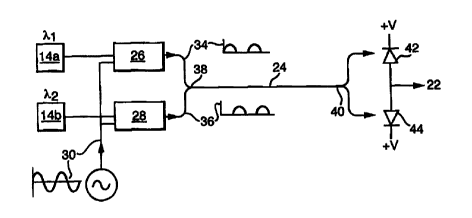
Referring now to Figure 2, this shows further detail of the modulator 12. The
light source
14 comprises first and second light sources 14a and 14b which produce light at
different
wavelengths 7~1 and 7~,~ respectively. In one embodiment they are
semiconductor lasers
operating around 1.SS~.m. The first light source 14a supplies a first sub-
modulator 26 and
the second light source I4b supplies a second sub-modulator 28. The sub-
modulators are
each fed with a modulating signal 30 which is the original electrical varying
signal. The
voltage of the modulating signal 30 varies in magnitude and has positive and
negative
components. In this example it is shown as a sine wave although in a practical
embodiment
a more complicated signal would be present.
The sub-modulator 26 is configured such that it modulates light from the light
source 14a
only when the modulating signal is varying in a range between zero and a
positive value.
The sub-modulator 28 is configured such that it modulates light from the light
source 14b
only when the modulating signal is varying in a range between zero and a
negative value.
Operation of the sub-modulators 26 and 28 is best explained with reference to
Figure 3.
This is a graph showing the operating characteristics of an electro-absorption
modulator
device which is an integral part of each of the sub-modulators 26 and 28. The
graph is a
plot of optical transmission against voltage. At low voltages most or all of
the light is
transmitted until a threshold voltage is reached at which no light is
transmitted. In order
to minimise distortion of the transmitted light, particularly if it is
modulated with analogue
signals, it is preferred that the device is operated in an operating region
where there is a
linear rclationship between transmission and voltage. As has been explained in
the
foregoing, each sub-modulator 26, 28 modulates light only when either a
positive or a
AMENDED SHEET
CA 02319482 2000-08-03
14-02-2000 GB 009900376
~ ~ ~ . .. .. .. ..
~. .. .. . . . . . . . .
. . . . . . . . . . ..
.... . . . . . . . .
. . . . . . . . ..
... . .. .... .. ..
8
negative voltage is applied. Therefore operating region 30 is defined by
biasing the
modulator with a fixed DC voltage in order to obtain the desired operating
characteristics.
As an example, the sub-modulator 28 is biased such that its nominal OV point
is at point
32. As a result, it will only transmit light when a negative voltage is
applied and will not
transmit light when a positive voltage is applied. Since there is a modulated
linear
transmission/voltage relationship below point 32, the sub-modulator 28
produces a
modulated light signal 36 which is a direct analogue of the negative part of
the original
varying electrical signal.
It is straightforward to configure the suh-modulator 26 so that it only
produces a response
for positive applied voltages. In order to obtain what is effectively the
mirror-image of the
operating characteristics of Figure 3, the drive signal of the sub-modulator
26 is inverted
That is, the sub-modulators 26 and 28 are driven in anti-phase to each other.
Suitable
biasing provides a nominal OV point below which the sub-modulator 26 will not
transmit
light and above which it will transmit light in proportion to the applied
voltage.
The level of second order distortion in the reproduced original varying
electrical signal can
be controlled and thus reduced to a negligible level provided that there is no
phase or
amplitude imbalance between the first and second varying optical signals when
they are
detected.
The sub-modulators 26 and 28 produce respective modulated optical signals 34
and 36 at
different wavelengths ~.I and 7~,z. In this example schematic waveforms are
shown
approximating to those which would be generated if the original varying
electrical signal
AMENDED SHEET
CA 02319482 2000-08-03
14-02-2000 GB 009900376
.. .. .. ..
.. .. .. . . . . . . . .
. . . . . . . . . . ..
- ~ ~ . .... . . . . . . . .
..
... . .. .... .. ..
9
16 is a sine wave. Obviously, since it is not possible to have "negative"
light, both optical
signals 34 and 36 have positive values. These signals are multiplexed onto the
optical fibre
24 with a coupler 38.
In this embodiment, the optical fibre 24 requires no special properties and so
can be of a
conventional type. The invention is therefore particularly suitable for use in
upgrading
existing optical links. At the demodulator, a wavelength dependent coupler 40
is used to
separate, that is demultiplex, the two signals 34 and 36.
The two optical signals are transported to the demodulator 18 which comprises
a suitable
photoreceiver. In a preferred embodiment the photoreceiver consists of two
photodiodes
42 and 44 configured so as to produce a combined output 22 which is identical
to the
original varying electrical signal 16. As shown in Figure 2 both photodiodes
are reverse
biased and are connected back to back, that is their cathodes are connected
together and the
combined output 22 is derived from the common connection.
In the embodiment shown in Figure 2 the sub-modulators 26 and 28 use different
light
sources 14a and 14b which supply light at different wavelengths. However, in
another
embodiment, a single light source is used to supply light to each of the sub-
modulators.
The single light source supplies an optical coupler which has output ports
connected to
each of the sub-modulators. In this embodiment the two signals 34 and 36 are
of the same
wavelength and so need to be differentiated in some way. This can be done by
placing
them in different polarisation states such as orthogonal polarisation states.
The signals 34
and 36 are then transmitted in a polarising maintaining (P1V17 fibre which
maintains their
AMENDED SHEET
CA 02319482 2000-08-03
14-02-2000 GB 009900376
.. .. .. ..
.. .. .. . . . . . . . .
. . . . . . . . . . ..
.... . . . . . . . .
..
... . .. .... .. ..
polarisation states by each having a different propagation velocity. A typical
PM fibre will
produce a time delay error of less than 0.6ps if it is less than O.Sm long.
This is equivalent
to a phase error of 4°. It is therefore necessary to compensate for
this effect. One
technique is to cut the PM fibre in half and splice the halves together with a
90 ° rotation
5 to swap the polarisation modes in the fibre. Demultiplexing at the
demodulator 18 requires
a polarisation splitter device such as a polarising beam sputter.
Of course, the sub-modulators 26 and 28 can send their respective optical
signals down
respective optical fibres to avoid the need for multiplexing and
demultiplexing. However,
10 a single optical fibre 24 is preferred to reduce the likelihood of there
being a path length
imbalance.
The SNR of such an optical link is greater than alternative approaches because
there is
substantially no unmodulated optical power arriving at either photodiode.
Compared to a
typical high performance optical link the invention can improve the SNR by
more than
lOdB.
The mean optical power on either photodiode is relatively small, because it is
dependent
only upon the magnitude of the modulating signal. This means that the noise
power out of
the links is not constant, but rather varies with drive power. The limiting
noise power at
low signal levels is now the thermal noise of the photoreceiver, which means
that the
dynamic range is increased relative to the known optical links. Optically
generated noise
(shot noise and RI1~ is therefore only apparent at vcry high drive powers.
AMENDED SHEET
CA 02319482 2000-08-03
14-02-2000 G B 009900376
~ ~ ~ ~ .. .. .. ..
~. .. .. . . .. . . ..
. . . . . . . . . . ..
- ~ . . .... . . . . . . . .
~ ~ ~ . . . . . ..
~ . ... . .. .... .. ..
11
The invention may provide an optical Link in which the CDR can be increased
due to
reduced optical power being detected by the detector. At present the known
direct
detection links are limited since the mean optical power they detect is close
to the
compression limit of each photodiode. In contrast in the optical link of the
present
invention the mean optical power is reduced and therefore the source power can
be
increased thereby increasing the CDR by a corresponding amount.
The invention provides an optical link configuration which minimises the level
of standing
optical power in a modulated optical signal and therefore minimises optically
generated
noise power.
AMENDED SHEET