Note: Descriptions are shown in the official language in which they were submitted.
CA 02319506 2000-08-03
WO 99140624 PCT/IL99/00071
INTEGRATED CIRCUIT DEVICE
1
FIELD OF THE INVENTION
The present invention relates to methods and
apparatus for producing integrated circuit devices and to
integrated circuit devices produced thereby and more
particular7.y to an optronic integrally packaged die.
BACKGRc)UND OF THE INVENTION
An essential step in the manufacture of all
integrated circuit devices is known as "packaging" and
involves mechanical and environmental protection of a
silicon clip which is at the heart of the integrated
circuit as well as electrical interconnection between
predetermine;. locations on the silicon chip and external
electrical terminals.
1~t present three principal technologies are
employed for packaging semiconductors: wire bonding, tape
automatic bonding (TAB) and flip chip.
Wire bonding employs heat and ultrasonic energy
to weld go7.d bonding wires between bond pads on the chip
and contacts on the package.
'rape automatic bonding (TAB) employs a copper
foil tape instead of bonding wire. The copper foil tape
is configured for each specific die and package combina-
tion and includes a pattern of copper traces suited
thereto. The individual leads may be connected individu-
ally or as a group to the various bond pads on the chip.
L~lip chips are integrated circuit dies which
have solder Dumps farmed on top of the bonding pads, thus
allowing i:he, die tc~ be "flipped" circuit side down and
directly soldered to a substrate. Wire bonds are not
required and considerable savings in package spacing may
be realized.
CA 02319506 2000-08-03
WO 99/40624 PCT/IL99/00071
2
The above-described technologies each have
certain limitations. Both wire bonding and TAB bonding
are prone to bad bond formation and subject the die to
relatively high temperatures and mechanical pressures.
Both wire bond and TAB technologies are problematic from
a package size viewpoint, producing integrated circuit
devices having a die-to-package area ratio ranging from
about 10% to 60%.
The flip-chip does not provide packaging but
rather only interconnection. The interconnection encoun-
ters problems of uniformity in the solder bumps as well
as in thermal expansion mismatching, which limits the use
of available substrates to silicon or materials which
have thermal expansion characteristics similar to those
of silicon.
Optronic packages for semiconductors are known.
Conventional optronic packages used for imaging employ a
ceramic housing onto which is sealingly mounted a trans-
parent window. Optronic packages used for low level
imaging, light emission and radiation detection, includ-
ing light detection, employ a clear plastic enclosure.
Described in applicant's published PCT Applica-
tion WO 95/19645 are methods and apparatus for producing
integrated circuit devices, including, inter alia, inte-
grally packaged dies having a radiation transparent
protective layer.
CA 02319506 2000-08-03
WO 99/40624 PCT/IL99/00071
3
SUMMARY OF THE INVENTION
The present invention seeks to provide optronic
integrated circuit devices which are extremely compact as
well as apparatus and techniques for the production
thereof .
There is thus provided in accordance with a
preferred embodiment of the present invention an inte-
grally packaged optronic integrated circuit device
including:
an integrated circuit die containing at least
one of a radiation emitter and radiation receiver and
having top and bottom surfaces formed of electrically
insulative and mechanically protective material, at least
one of the surfaces being transparent to radiation, and
electrically insulative edge surfaces having pads.
Preferably, the device~also includes at least
one spectral filter associated with a radiation transpar-
ent protective surface thereof.
Additionally in accordance with a preferred
embodiment of the present invention, the device includes
a semiconductor substrate which is sufficiently thin as
to enable to device to be responsive to back illumina-
tion.
Preferably, the device also includes at least
one color filter associated with a radiation transparent
protective surface thereof.
Further in accordance with a preferred embodi-
ment of the present invention, lenses may be integrally
formed on a transparent protective surface of the device.
Additionally in accordance with a preferred
embodiment of the present invention, light coupling bumps
may be integrally formed on a transparent protective
surface of the device.
Further in accordance with a preferred embodi-
ment of the present invention a waveguide and other
CA 02319506 2000-08-03
WO 99/40624 PCT/IL99/00071
4
optical components integrally formed on a transparent
protective surface of the device.
Additionally in accordance with a preferred
embodiment of the present invention, an optical grating
may be integrally formed on a transparent protective
surface of the device.
Further in accordance with a preferred embodi-
ment of the present invention a polarizer may be formed
on a transparent protective surface of the device.
There is also provided in accordance with a
preferred embodiment of the present invention an inte-
grally packaged optronic integrated circuit device
including:
an integrated circuit die containing at least
one of a radiation emitter and radiation receiver and
having top and bottom surfaces formed of electrically
insulative and mechanically protective material, at least
one of the surfaces being transparent to radiation, the
integrally packaged optronic integrated circuit device
being characterized in that its longest dimension does
not exceed the longest dimension of the die by more than
20%. Preferably the integrally packaged optronic inte-
grated circuit device is characterized in that its long-
est dimension does not exceed the longest dimension of
the die by more than 10%. More preferably the integrally
packaged optronic integrated circuit device is charac-
terized in that its longest dimension does not exceed the
longest dimension of the die by more than 5%.
There is also provided in accordance with a
preferred embodiment of the present invention a method
for producing an integrally packaged optronic integrated
circuit device comprising the steps of:
forming electrical circuits onto a
semiconductor wafer;
forming at least one transparent mechanical
protective layer onto said semiconductor wafer over said
CA 02319506 2000-08-03
WO 99/40624 PCT/IL99/00071
electrical circuits;
forming solderable contacts onto said
semiconductor wafer; and
thereafter, dicing said wafer into individual
packaged dies.
CA 02319506 2000-08-03
WO 99/40624 PCT/IL99/00071
6
BRIEF DESCRIPTION OF THE DRAWINGS
The present invention will be understood and
appreciated more fully from the following detailed de-
scription, taken in conjunction with the drawings in
which:
Figs. lA and 1B are respective top view and
bottom view simplified pictorial illustrations of an
integrally packaged optronic integrated circuit device
constructed and operative in accordance with a preferred
embodiment of the present invention;
Fig. 1C is a bottom view simplified pictorial
illustration of an integrally packaged optronic integrat-
ed circuit device of the type shown in Figs. lA and iB,
constructed and operative in accordance with another
preferred embodiment of the present invention;
Fig. 2 is a simplified pictorial illustration
of the attachment of a transparent protective packaging
layer to a wafer containing a plurality of integrated
circuit dies;
Fig. 3 is a simplified pictorial illustration
of showing the individual dies on the wafer as seen
through the transparent protective packaging layer
attached thereto;
Figs. 4A, 4B, 4C and 4D are sectional illustra-
tions of various stages in the manufacture of integrally
packaged optronic integrated circuit devices in accord-
ance with a preferred embodiment of the present inven-
tion;
Fig. 5 is a partially cut away detailed picto-
rial illustration of an integrally packaged optronic
integrated circuit device produced from the wafer of Fig.
4D;
Figs. 6, 7A, 7B, 8A and 8B are sectional illus-
trations of various stages in the manufacture of the
integrally packaged optronic integrated circuit device
shown in Figs. lA, 1B, 1C & 5;
CA 02319506 2000-08-03
WO 99/40624 PCT/IL99/00071
7
Figs. 9, i0A and lOB together provide a simpli-
fied block diagram illustration of apparatus for carrying
out the method of the present invention;
Figs. 11A, ilH, 11C, 11D and 11E are simplified
pictorial illustrations of five alternative embodiments
of an integrated circuit device constructed and operative
in accordance with yet another preferred embodiment of
the present invention and including spectral filters
and/or anti-reflective coatings;
Figs. 12A, 12B and 12C are simplified pictorial
illustrations of three alternative embodiments of an
integrally packaged optronic integrated circuit device
which is designed for back illumination;
Figs. 13A, 13B and 13C are simplified pictorial
illustrations of three alternative embodiments of an
integrally packaged optronic integrated circuit device
constructed and operative in accordance with still anoth-
er preferred embodiment of the present invention wherein
color array filters are integrated with the integrally
packaged optronic integrated circuit device;
Figs. 14A, 14B, 14C and 14D are simplified
pictorial illustrations of four alternative embodiments
of an integrally packaged optronic integrated circuit
device constructed and operative in accordance with
another preferred embodiment of the present invention
having lenses integrally formed on a transparent protec-
tive surface thereof;
Figs. 15A and 15B are simplified pictorial
illustrations of two alternative embodiments of an inte-
grally packaged optronic integrated circuit device con-
structed and operative in accordance with another pre-
ferred embodiment of the present invention having light
coupling bumps integrally formed on a transparent protec-
tive surface thereof;
Figs. I6A and 1sB are simplified pictorial
illustrations of two alternative embodiments of an inte-
CA 02319506 2000-08-03
WO 99/40624 PCT/IL99/00071
8
grally packaged optronic integrated circuit device con-
structed and operative in accordance with yet another
preferred embodiment of the present invention having a
waveguide and other optical components integrally formed
on a transparent protective surface thereof;
Figs. 17A and 17B are simplified pictorial
illustrations of two alternative embodiments of an inte-
grally packaged optronic integrated circuit device con-
structed and operative in accordance with still another
preferred embodiment of the present invention wherein a
polarizes is integrated with the integrally packaged
optronic integrated circuit device;
Figs. 18A and 18B are simplified pictorial
illustrations of two alternative embodiments of an inte-
grally packaged optronic integrated circuit device con-
structed and operative in accordance with still another
preferred embodiment of the present invention wherein an
optical grating is integrated with the integrally pack-
aged optronic integrated circuit device.
Figs. 19A and 19B are simplified pictorial
illustrations of two alternative embodiments of an inte-
grally packaged optronic integrated circuit device con-
structed and operative in accordance with yet another
preferred embodiment of the present invention wherein the
package is formed with a desired geometrical
configuration;
Figs. 20A and 2oB are simplified pictorial
illustrations of two alternative embodiments of an inte-
grally packaged optronic integrated circuit device con-
structed and operative in accordance with yet another
preferred embodiment of the present invention wherein
edges of the package are coated with an opaque coating;
Fig. 21 is a simplified pictorial illustration
of an integrally packaged optronic integrated circuit
device constructed and operative in accordance with still
another preferred embodiment of the present invention and
CA 02319506 2000-08-03
WO 99/40624 PCT/IL99/00071
9
having an octagonal configuration; and
Fig. 22 is a simplified pictorial illustration
of a cutting pattern employed to produce integrated
circuits of the type shown in Fig. 21.
CA 02319506 2000-08-03
WO 99/40624 PCT/IL99/00071
DETAILED DESCRIPTION OF PREFERRED EMBODIMENTS
Reference is now made to Figs. lA - 22, which
illustrate the production of integrated circuit devices
in accordance with a preferred embodiment of the present
invention.
Figs. 1A and 1B together illustrate a preferred
embodiment of integrated circuit device constructed and
operative in accordance with a preferred embodiment of
the present invention. The integrated circuit device
includes a relatively thin and compact, environmentally
protected and mechanically strengthened integrated cir-
cuit package l0 having a multiplicity of electrical
contacts 12 plated along the edge surfaces 14 thereof.
In accordance with a preferred embodiment of
the invention, contacts 12 extend over edge surfaces onto
the planar surfaces 16 of the, package. This contact
arrangement permits both flat surface mounting and edge
mounting of package 10 onto a circuit board. It is noted
that the integrated circuit package 10 may include one or
more of the following elements (not shown): an integrally
formed dichroic filter, color filter, antireflective
coating, polarizes, optical grating, integrated wave
guide and optical coupling bumps.
Fig. 1C illustrates an alternative embodiment
of the present invention wherein solderable bumps 17 are
provided at the ends of each contact 12. Preferably, the
solderable bumps 17 are arranged in a predetermined
array.
In accordance with a preferred embodiment of
the present invention, and as illustrated in Fig. 2 and
Fig. 4A, a complete silicon wafer 20 having a plurality
of finished dies 22 formed thereon by conventional tech-
niques, is bonded at its active surface 24 to a radiation
transparent protective insulating cover plate 26 via a
layer 28 of epoxy. The insulating cover plate 26 typical-
CA 02319506 2000-08-03
WO 99/40624 PCT/IL99/00071
11
ly comprises glass, quartz, sapphire or any other suit-
able radiation transparent insulative substrate.
The cover plate 26 may be colored or tinted in
order to operate as a spectral filter. Alternatively, a
dichroic or colored spectral filter may be formed on at
least one surface of the cover plate 26.
It is a particular feature of the present
invention that cover plate 26 and epoxy layer 28 are
preferably transparent to radiation in a spectral region
useful for optronic applications.
It is appreciated that certain steps in the
conventional fabrication of silicon wafer 20 may be
eliminated when the wafer is used in accordance with the
present invention. These steps include the provision of
via openings above pads, wafer back grinding and wafer
back metal coating.
The complete silicon wafer 20 may be formed
with an integral color filter array by conventional
lithography techniques at any suitable location therein.
Prior to the bonding step of Fig. 4A, a filter may be
formed and configured by conventional techniques over the
cover plate 26, such that the filter plane lies between
cover plate 26 and the epoxy layer 28.
Following the bonding step .described hereina-
bove, the.silicon wafer is preferably ground down to a
decreased thickness, typically 100 microns, as shown in
Fig. 4B. This reduction in wafer thickness is enabled by
the additional mechanical strength provided by the bond-
ing thereof of the insulating cover plate 26.
Following the reduction in thickness of the
wafer, which is optional, the wafer is etched, using a
photolithography process, along its back surface along
predetermined dice lines which separate the individual
dies. Etched channels 30 are thus produced, which extend
entirely through the thickness of the silicon substrate,
typically 100 microns. The etched wafer is shown in Fig.
CA 02319506 2000-08-03
WO 99/40624 PCT/IL99/00071
12
4C.
The aforementioned etching typically takes
place in conventional silicon etching solution, such as a
combination of 2.5% hydrofluoric acid, 50% nitric acid,
10% acetic acid and 37.5% water, so as to etch the sili-
con down to the field oxide layer, as shown in Fig. 4C.
The result of the silicon etching is a plurali-
ty of separated dies 40, each of which includes silicon
of thickness about 100 microns.
As seen in Fig. 4D, following the silicon
etching, a second insulating packaging layer 42 is bonded
over the dies 40 on the side thereof opposite to insulat-
ing packaging layer 26. A layer 44 of epoxy lies between
the dies 40 and the layer 42 and epoxy also fills the
interstices between dies 40. In certain applications,
such as the embodiment of Figs. 12A - 12C, the packaging
layer 42 and the epoxy layer 44 are both transparent.
The sandwich of the etched wafer 20 and the
first and second insulating packaging layers 26 and 42 is
then partially cut along lines 50, lying along the inter-
stices between adjacent dies 40 to define notches along
the outlines of a plurality of pre-packaged integrated
circuits. It is a particular feature of the invention
that lines 50 are selected such that the edges of the
dies along the notches are distanced from the outer
extent of the silicon 40 by at least a distance d, as
shown in Figs. 4D and 5, to which reference is now addi-
tionally made.
It is a particular feature of the present
invention that partial cutting of the sandwich of Fig. 4D
along lines 50 exposes edges of a multiplicity of pads 34
on the wafer 20, which pad edges, when so exposed, define
contact surfaces 51 on dies 40.
Referring now particularly to Fig. 5, at least
one insulating layer, including the field oxide layer, is
shown at reference numeral 32 and metal pads are shown
CA 02319506 2000-08-03
WO 99/40624 PCT/IL99/00071
13
at reference numeral 34. An over-metal insulating layer
is shown at reference numeral 36. The color filter plane
is shown at reference numeral 38.
Reference is now made to Figs. 6, 7A, 7B, 8A
and 8B, which illustrate further steps in the manufacture
of integrated circuit devices in accordance with a pre-
ferred embodiment of the present invention.
Fig. 6 illustrates at reference numeral 54, a
preferred cross sectional configuration of a notch pro-
duced by partially cutting as described hereinabove in
connection with Fig. 5. Vertical lines 56 indicate the
intersection of the notch 54 with the pads 34, defining
exposed sectional pad surfaces 51. Vertical lines 58
indicate the location of a subsequent final cut which
separates the dies into individual integrated circuits at
a later stage.
Figs. 7A and 7B illustrate the formation of
metal contacts 12 along the inclined edges 14 and part of
the top surface 16. These contacts, which may be formed
by any suitable metal deposition technique, are seen to
extend inside notch 54, thus establishing electrical
contact with surfaces 51 of pads 34. Fig. 7A shows a
configuration corresponding to that of Figs. lA and 1B
without solderable bumps, while Fig. 7B shows the
provision of solderable bumps 17 on contacts 12, as
illustrated in Fig. 1C.
It is a particular feature of the present
invention that metal contacts are formed onto the dies in
electrical contact with surfaces 51 of pads 34 without
first separating the dies into individual chips.
Figs. 8A and 8B illustrate subsequent dicing of
the individual dies on the wafer, subsequent to metal
contact formation thereon, into individual pre-packaged
integrated circuit devices. Fig. 8A shows a configura-
tion corresponding to that of Figs. lA and 1B without
solderable bumps, while Fig. 8B shows the provision of
CA 02319506 2000-08-03
WO 99/40624 PCT/IL99/00071
14
solderable bumps 17 on contacts 12, as illustrated in
Fig. iC.
Reference is now made to Figs. 9, l0A and lOB,
which together illustrate apparatus for producing inte-
grated circuit devices in accordance with a preferred
embodiment of the present invention. A conventional wafer
fabrication facility 180 provides complete wafers 20.
Individual wafers 20 are bonded on their active surfaces
to protective layers, such as glass layers 26, using
epoxy 28, by bonding apparatus 182, preferably having
facilities for rotation of the wafer 20, the layer 26 and
the epoxy 28 so as to obtain even distribution of the
epoxy.
The bonded wafer (Fig. 3) is thinned at its
non-active surface as by grinding apparatus 184, such as
Model 32BTGW using 12.5A abrasive, which is commercially
available from Speedfam Machines Co. Ltd. of England.
The wafer is then-etched at its non-active
surface, preferably by photolithography, such as by
using conventional spin-coated photoresist, which is
commercially available from Hoechst, under the brand
designation AZ 4562.
The photoresist is preferably mask exposed by a
suitable W exposure system 185, such as a Rarl Suss
Model KSMA6, through a lithography mask 186 to define
etched channels 30.
The photoresist is then developed in a develop-
ment bath (not shown), baked and then etched in a silicon
etch solution 190 located in a temperature controlled
bath 188. Commercially available equipment for this
purpose include a Chemkleen bath and an WHRV circulator
both of which are manufactured by Wafab Inc. of the
U.S.A.. A suitable conventional silicon etching solution
is Isoform Silicon etch, which is commercially available
from Micro-Image Technology Ltd. of England. The wafer is
conventionally rinsed after etching. The resulting etched
CA 02319506 2000-08-03
WO 99/40624 PCT/IL99/00071
wafer is shown in Fig. 4C.
Alternatively, the foregoing wet chemical
etching step may be replaced by dry plasma etching.
The etched wafer is bonded on the non-active
side to another protective layer 42 by bonding apparatus
192, which may be essentially the same as apparatus 182,
to produce a doubly bonded wafer sandwich as shown in
Fig. 4D.
Notching apparatus 194 partially cuts the
bonded wafer sandwich of Fig. 4D to a configuration shown
in Fig. 5.
The notched wafer is then subjected to anti-
corrosion treatment in a bath 196, containing a chromat-
ing solution 198, such as described in any of the follow-
ing U.S. Patents: 2,507,956; 2,851,385 and 2,796,370, the
disclosure of which is hereby incorporated by reference.
Conductive layer deposition apparatus 200,
which operates by vacuum deposition techniques, such as a
Model 903M sputtering machine manufactured by Material
Research Corporation of the U.S.A., is employed to pro-
duce a conductive layer on one or more surfaces of each
die of the wafer as shown in Fig. 7.
Configuration of contact strips, as shown in
Fig. 7, is carried out preferably by using conventional
electro-deposited photoresist, which is commercially
available from DuPont under the brand name Primecoat or
from Shipley, under the brand name Eagle. The photoresist
is applied to the wafers in a photoresist bath assembly
202 which is commercially available from DuPont or Ship-
ley.
The photoresist is preferably light configured
by a UV exposure system 204, which may be identical to
system 185, using a mask 205 to define suitable etching
patterns. The photoresist is then developed in a develop-
ment bath 206, and then etched in a metal etch solution
208 located in an etching bath 210, thus providing a
CA 02319506 2000-08-03
WO 99/40624 PCT/IL99/00071
16
conductor configuration such as that shown in Figs. lA
and 1B.
The exposed conductive strips shown in Fig. 7
are then plated, preferably by electroless plating appa-
ratus 212, which is commercially available from Okuno of
Japan.
The wafer is then diced into individual pre-
packaged integrated circuit devices. Preferably the
dicing blade 214 should be a diamond resinoid blade of
thickness 4 - 12 mils. The resulting dies appear as
illustrated generally in Figs. lA and 1B.
Fig. l0A shows apparatus for producing an
integrated circuit configuration corresponding to that of
Figs. lA and iB without solderable bumps, while Fig. lOB
shows apparatus for producing an integrated circuit
configuration corresponding to that of Fig. 1C having
solderable bumps. The embodiment of Fig. lOB is identical
to that of Fig. 10A, apart from the additional provision
of bump forming apparatus 213 downstream of the
electroless plating apparatus 212.
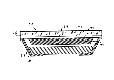
Reference is now made to Figs. 11A - 11E, which
illustrate five alternative preferred embodiments of
integrated circuit device constructed and operative in
accordance with another preferred embodiment of the
present invention and includes a relatively thin and
compact, environmentally protected and mechanically
strengthened integrated circuit package 310 having a
multiplicity of electrical contacts 312 plated along the
edge surfaces 314 thereof.
Fig. 11A shows a dichroic filter and/or anti-
reflective coating 315 formed on an outer facing surface
316 of a transparent protective layer 317. Fig. 11B
illustrates a coating 318, which may be identical to
coating 315, which is formed on an inner facing surface
319 of transparent protective layer 317. Fig. 11C shows
both coatings 315 and 318 on respective surfaces 316 and
CA 02319506 2000-08-03
WO 99/40624 PCT/IL99/00071
17
319 of transparent protective layer 317. Optronic
components are formed on a surface 320 of a silicon
substrate 322 of conventional thickness, typically loo
microns. Surface 320 faces transparent protective layer
317.
Fig. 11D shows an absorption filter 323 formed
on outer facing surface 316 of transparent protective
layer 317. Fig. 11E shows an absorption filter 323,
having formed thereon an anti-reflective coating 324,
formed on outer facing surface 316 of transparent protec-
tive layer 317.
Reference is now made to Figs. 12A - 12C, which
illustrate three alternative preferred embodiments of
integrated circuit device which include a relatively thin
and compact, environmentally protected and mechanically
strengthened integrated circuit package 330 having a
multiplicity of electrical contacts 332 plated along the
edge surfaces 334 thereof .
In contrast to the embodiments of Figs. 11A -
11E, the integrated circuit devices of Figs. 12A - 12C
are designed for back illumination and therefore employ a
thinned silicon substrate 336, typically having a thick-
ness of 12 - 15 microns.
Whereas in the embodiment of Figs..llA - 11E,
the optronic components are formed on a surface 320 which
faces a transparent protective layer 317, in the
embodiment of Figs. 12A - 12B, the components may be
formed on a surface 340 of substrate 336, which surface
340 faces away from the corresponding transparent
protective layer 337. The extreme thickness of the sub-
strate 336 in the embodiments of Figs. 12A - 12C enables
the optronic components on surface 340 to be exposed to
light impinging via transparent protective layer 337 by
back exposure.
It is appreciated that silicon is transparent
to certain radiation spectra, such as IR radiation. When
CA 02319506 2000-08-03
WO 99/40624 PCT/IL99/00071
18
an IR responsive device is provided, the embodiment of
Figs. 12A - 12C can be constructed without a thinned
silicon substrate.
Fig. 12A shows a dichroic filter and/or anti-
reflective coating 345 formed on an outer facing surface
346 of the transparent protective layer 337. Fig. 12B
illustrates a coating 348, which may be identical to
coating 345, which is formed on an inner facing surface
349 of transparent protective layer 337. Fig. 12C shows
both coatings 345 and 348 on respective surfaces 346 and
349 of transparent protective layer 337.
The modifications shown in Figs. 11D and 11E
may also be embodied in the configuration of Figs. 12A -
12C.
Reference is now made to Figs. 13A, 13B and
13C, which illustrate three alternative preferred embod-
iments of integrated circuit device constructed and
operative in accordance with another preferred embodiment
of the present invention and includes a relatively thin
and compact, environmentally protected and mechanically
strengthened integrated circuit package 350 having a
multiplicity of electrical contacts 352 plated along the
edge surfaces 354 thereof.
Fig. 13A shows a color filter, such as an RGB
or masking filter, 355 formed on an outer facing surface
356 of a transparent protective layer 357. Fig. 13B
illustrates a filter 358, which may be identical to
filter 355, which is formed on an outer facing surface
359 of a silicon substrate 362. Fig. 13C shows both
filters 355 and 358 on respective surfaces 356 and 359.
It is appreciated that filter 356 may
alternatively be located on an inner facing surface of
transparent protective layer 357.
Reference is now made to Figs. 14A, 148, 14C
and 14D, which illustrate four alternative embodiments of
an integrally packaged optronic integrated circuit device
CA 02319506 2000-08-03
WO 99/40624 PCT/IL99/OOO~t
19
constructed and operative in accordance with another pre-
ferred embodiment of the present invention having lenses
integrally formed on a transparent protective surface
thereof.
The embodiment of Fig. 14A may be identical to
that of Fig. 11A without the coating and is further
distinguished therefrom in that it has a transparent
protective layer 370 which is formed with an array of
microlenses 372 on an outer facing surface 374 thereof.
The embodiment of Fig. 14B may be identical to
that of Fig. 12A without the coating and is further
distinguished therefrom in that it has a transparent
protective layer 380 which is formed with an array of
microlenses 382 on an outer facing surface 384 thereof.
In the illustrated embodiment of Figs. 14A and
14B, the microlenses 372 and 382 respectively are formed
of the same material as than of transparent protective
layers 370 and 380 respectively. Alternatively,
microlenses 372 and 382 may be formed of a material
different from that of respective transparent protective
layers 370 and 380.
The embodiment of Fig. 14C corresponds to that
of Fig. 14A. However in the embodiment of Fig. 14C, an
array of microlenses 385 is formed on an inner facing
surface of transparent protective layer 370. In the
illustrated embodiment of Fig. 14C, the microlenses 385
are formed of a different material than of transparent
protective layer 370. Alternatively, microlenses 385 may
be formed of the same material as that of transparent
protective layer 370.
The embodiment of Fig. 14D corresponds to that
of Fig. 14B. However in the embodiment of Fig. 14D,
similarly to the embodiment of Fig. 14C, an array of
microlenses 387 is formed on an inner facing surface of
transparent protective layer 380. In the, illustrated
embodiment of Fig. 14D, the microlenses 387 are formed of
CA 02319506 2000-08-03
WO 99/40624 PCT/1L99/000?1
a different material than of transparent protective layer
380. Alternatively, microlenses 387 may be formed of the
same material as that of transparent protective layer
380.
In the embodiments of Figs. 14C and 14D, the
index of refraction of the microlenses 385 and 387
respectively must exceed that of an epoxy layer 388
underlying them.
Reference is now made to Figs. 15A and 15B,
which are simplified pictorial illustrations of two
alternative embodiments of an integrally packaged optron--
ic integrated circuit device constructed and operative in
accordance with another preferred embodiment of the
present invention having light coupling bumps integrally
formed on a transparent protective surface thereof.
The embodiment of Fig. 15A may be identical to
that of Fig. 11A without the coating and is further
distinguished therefrom in that it has a light coupling
bump 390 formed on a transparent protective layer 392. A
waveguide 394 is shown optically coupled to the
transparent protective layer 392 via bump 390. Preferably
the bump 390 is formed of a transparent organic material
which is somewhat compliant such that mechanical pressure
produces a slight deformation thereof and enables an
evanescent light wave to pass through an interface
defined therewith.
The embodiment of Fig. 15B may be identical to
that of Fig. 12A without the coating and is further
distinguished therefrom in that it has a light coupling
bump 396 formed on a transparent protective layer 398. A
waveguide 399 is shown optically coupled to the
transparent protective layer 398 via bump 396.
Reference is now made to Figs. 16A and 16B
which are simplified pictorial illustrations of two
alternative embodiments of an integrally packaged optron-
ic integrated circuit device constructed and operative in
CA 02319506 2000-08-03
WO 99/40624 PCT/IL99/00071
21
accordance with yet another preferred embodiment of the
present invention having a waveguide and other optical
components integrally formed on a transparent protective
surface thereof.
The embodiment of Fig. 16A may be identical to
that of Fig. 11A without the coating and is further
distinguished therefrom in that it has a wave guide 400
and possibly other optical elements (not shown) formed on
a transparent protective layer 402, as by conventional
integrated optics techniques. This arrangement enables
optical communication between an optronic component
formed on a silicon substrate 404 via the transparent
protective layer 402 and the wave guide 400.
The embodiment of Fig. 16B may be identical to
that of Fig. 12A without the coating and is further
distinguished therefrom in that it has a wave guide 410
and possibly other optical elements (not shown) formed on
a transparent protective layer 412, as by conventional
integrated optics techniques. This arrangement enables
optical communication between an optronic component
formed on a silicon substrate 414 via the transparent
protective layer 412 and the wave guide 410.
Reference is now made to Figs. 17A and 17B,
which are simplified pictorial illustrations of two
alternative embodiments of an integrally packaged optron-
ic integrated circuit device constructed and operative in
accordance with still another preferred embodiment of the
present invention wherein a polarizer is integrated with
the integrally packaged optronic integrated circuit
device.
The embodiment of Fig. 17A may be identical to
that of Fig. 11A without the coating and is further
distinguished therefrom in that it has a polarizer 420
which is on an outer facing surface 422 of a transparent
protective layer 424.
The embodiment of Fig. 17B may be identical to
CA 02319506 2000-08-03
WO 99/40624 PC'T/IL99/00071
22
that of Fig. 12A without the coating and is further
distinguished therefrom in that it has a polarizes 430
which is on an outer facing surface 432 of a transparent
protective layer 434.
Reference is now made to Figs. 18A and 18B,
which are simplified pictorial illustrations of two
alternative embodiments of an integrally packaged optron-
ic integrated circuit device constructed and operative in
accordance with still another preferred embodiment of the
present invention wherein an optical grating is integrat-
ed with the integrally packaged optronic integrated
circuit device.
The embodiment of Fig. i8A may be identical to
that of Fig. 11A without the coating and is further
distinguished therefrom in that it has a transparent
protective layer 440 which is formed with an optical
grating 442 on an outer facing surface 444 thereof.
The embodiment of Fig. 18B may be identical to
that of Fig. 12A without the coating and is further
distinguished therefrom in that it has a transparent
protective layer 450 which is formed with an optical
grating 452 on an outer facing surface 454 thereof.
Reference is now made to Figs. 19A and 19B
which may be generally similar in all relevant respects
to respective Figs. 11A and 12A respectively. The embodi-
ment of Figs. 19A and 19B is characterized in that a
transparent protective layer 460 is provided with a
particular edge configuration, preferably to enable it to
be located in an aperture. In Figs. 19A and 19B, the
transparent protective layer 460 is shown with a periph-
eral edge defining a step 462. It is appreciated that any
other suitable configuration may also be provided for
the transparent protective layer 460.
Reference is now made to Figs. 20A and 20B,
which are simplified pictorial illustrations of two
alternative embodiments of an integrally packaged optron-
CA 02319506 2000-08-03
WO 99/40624 PCT/IL99/00071
23
is integrated circuit device constructed and operative in
accordance with yet another preferred embodiment of the
present invention wherein edges of the package are coated
with an opaque coating.
The embodiment of Fig. 20A may correspond to
that of Fig. 19A wherein the transparent protective layer
460 may be provided with an opaque coating 464 at its
peripheral edge which may cover step 462 and may also
cover the edge of the outer facing surface adjacent
thereto.
The embodiment of Fig. 20B may correspond
generally to that of Fig. 11A wherein a transparent
protective layer 470 may be provided with an opaque
coating 472 at its peripheral edge which may also cover
the edge of the outer facing surface adjacent thereto.
Reference is now made to Fig. 21, which is a
simplified pictorial illustration of an integrally pack-
aged optronic integrated circuit device constructed and
operative in accordance with still another preferred
embodiment of the present invention and having an octago-
nal configuration. This configuration is preferred for
compact applications, such as endoscopes which a high
density of focal plane sensors and electronics is
required.
Fig. 22 is a simplified pictorial illustration
of a cutting pattern employed to produce integrated
circuits of the type shown in Fig. 21. The cutting
pattern of Fig. 22, which is shown overlaid on a wafer
480, comprises six consecutive cuts for each die.
It will be appreciated by persons skilled in
the art that the present invention is not limited to what
has been particularly shown and described hereinabove.
Rather the scope of the present invention includes both
combinations and subcombinations of the various features
described hereinabove as well as modifications and
variations thereof as would occur to a person of skill in
CA 02319506 2000-08-03
WO 99/40624 PCT/IL99/00071
24
the art upon reading the foregoing specification and
which are not in the prior art.