Note: Descriptions are shown in the official language in which they were submitted.
CA 02319696 2000-09-27
1030P9CAD2
METHODS OF LEARNING THE CHARACTERISTICS OF A TELEPHONE
This invention relates to the field of telephony. More particularly, this
invention relates
to methods of learning the characteristics of a telephone.
For purposes of this discussion, a telephone network can be considered as
being divided
into two parts. The first part comprises everything from the telephone company
leading
up to and including the Central Office (CO) termination point in a
subscriber's home or
office. The second part comprises everything from the Central Office
termination point
and includes the individual telephone sets connected directly to this
termination point as
well as proprietary systems (Key/PBX) and their respective proprietary
telephone sets.
Everything within the first part is regulated, in the United States of
America, by the
Federal Communications Commission (FCC) and therefore has a standard to which
telephone set and system manufacturers must base their interface equipment.
This
includes all devices connecting directly to the Central Office telephone
network,
including telephone sets and telephone systems. One problem that the telephony
industry
faces is that the other parts of the telephone network are not regulated,
including anything
related to the telephone sets which is not connected directly to the telephone
network,
such as proprietary telephone sets and all hand sets.
Private phones generally include a telephone base unit and modular
accessories, such as
a handset/headset. Accordingly, telephone manufacturers can and do develop
independent interface systems between their telephone base units and
accessories such
as handsets/headsets. This often precludes the use of a different type of
handset/headset
with a particular base unit without manual reprogramming. The problem is
especially
apparent when dealing with Key and Private Branch Exchange (PBX) system
station sets
which are entirely proprietary in nature. Many manufacturers are providing
accessories
which are provided as original equipment with the base unit. Many of these
accessory
products provide both voice and data solutions not offered in the telephone
station sets
such as headset, teleconferencing, facsimile and modem communication
alternatives.
CA 02319696 2000-09-27
-2-
What is needed is an invention that will allow a user to automatically
calibrate a
commercially available non-regulated voice/data product to allow an effective
interface.
This would solve any incompatibility problems and provide users with greater
choices
and flexibility when selecting telephone equipment.
It is accordingly an object of the present invention to counteract interface
problems
between proprietary handset ports on telephone base units and voice/data
accessory
products by allowing a user to automatically calibrate the telephone accessory
product
for an optimal interface match with the intended telephone base unit.
According to one aspect of the present invention, there is provided a Host
Automated 800
Learning Sequence method of learning the characteristics of any telephone with
a 4-wire
port interface which comprises the steps o~
a. searching for a DTMF tone by a host;
b. sending a preamble to a user;
c. disabling a reference signal;
d. enabling a level detect system;
e. measuring an incoming transmit signal;
f. comparing the transmit signal against a transmit level reference;
g. sending a level confirmation signal.
According to another aspect of the present invention, there is provided an SIT
Automated
800 Learning Sequence method of learning the characteristics of any telephone
with a 4-
wire port interface which comprises the steps of:
CA 02319696 2000-09-27
-3-
a. searching for a preamble;
b. detecting the preamble;
S c. selecting receive lines;
d. setting the receive lines' channel sensitivity by comparison with receive
level references;
e. selecting transmit lines; and
f. setting the transmit lines' channel sensitivity by comparison with a
transmit reference signal.
The invention will be more readily understood from the following description
of an
embodiment thereof with reference to the accompanying drawings, in which:-
FIG. 1 illustrates a flow model of a "Central Office (CO) Dialtone Learning
Sequence."
FIG. 2 illustrates a flow model of the "Automated 800 Learning Sequence."
FIG. 3 illustrates a diagram of the SIT Data Transmission technique used for
the
"Automated 800" and "Manual 800" Learning.
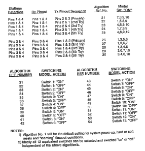
FIG. 4 illustrates switching algorithms for the system.
FIG. 5 is a continuation of the switching algorithms of FIG. 4.
FIG. 6 illustrates a block diagram of the regulated and non-regulated portions
of a typical
telephone interface configuration as it relates to both the Central Office and
the "Smart
Interface Technology" (SIT) system connection.
CA 02319696 2000-09-27
-4-
FIG. 7 illustrates a block diagram of the SIT system including a full-custom
analog and
semi-custom digital microcontroller integrated circuit.
FIG. 8 illustrates a block diagram of the SIT full-custom analog integrated
circuit.
FIG. 9 illustrates a block diagram of 4x4 crosspoint switch and shunt resistor
arrays.
FIG. 1 is a flow model of the "CO Dialtone Learning Sequence." This is the
primary
method the SIT system uses to "learn" the characteristics of the telephone
interface. The
"CO Dialtone Learning Sequence" is automatic and transparent to the end user.
Upon initial system power-up, such as the first time batteries are installed,
a "CO
Dialtone Search" routine is enabled to detect and locate a CO dialtone signal
on any
combination of the 4-wire interface lines from the telephone base unit. When
the CO
dialtone is detected, the "CO Dialtone Learning Sequence" will be fully
enabled.
The "CO Dialtone Learning Sequence" is a one time activation process. After a
successful "learn sequence" has been executed, the appropriate bit addressable
latch 1
settings are stored from the digital MCU 100 into the EEPROM 300, in order to
maintain
the correct settings in the event of a power failure. Subsequent CO dialtones
will not
enable the learning sequence unless a system reset is performed to re-enable
the learning
routine. The "CO Dialtone Learning Sequence" is re-enabled by a user
depressing the
system reset switch 258 for a minimum of five seconds or by a soft system
reset which
is accessed remotely.
The "CO Dialtone Learning Sequence" starts with the location of the CO
dialtone.
Location of the CO dialtone indicates the proper receive lines. The receive
input step
attenuator then adjusts the receive channel sensitivity based on reference
levels as
described above. The transmit lines are then selected and the transmit output
step
attenuator adjusts the transmit channel sensitivity based on reference levels.
CA 02319696 2000-09-27
-5-
FIG. 2 illustrates the flow models of the SIT "Automated 800 Learning
Sequence." Due
to the lack of regulation as it relates to Key and PBX system station sets,
there is a wide
variation of sidetone characteristics which may be encountered. Consequently,
it is
possible that occasionally, the learning method employed by the "CO Dialtone
Method"
may not provide optimal overall SIT system performance. The "Automated 800
Method"
provides a very accurate means for the SIT system to "learn" the
characteristics of a 4-
wire telephone port interface.
The "Automated 800 Learning Method" involves interaction between a "Host"
system
located at the termination of the accessed telephone line and the "SIT" system
located at
the end user's location. The user places a call to a designated telephone
number and is
greeted by an "automated attendant" message. In the case of a voice
application such as
a headset interface, the message instructs the user to momentarily depress the
system
reset switch 258, place the "handset/headset" switch to the "headset" position
and press
a key on the telephone set keypad. The keystroke interrupts the "auto
attendant" message
and the "Host" sends a preamble to the "SIT" system. When the preamble is
detected, the
"Automated 800 Learning Method" is enabled.
The "Automated 800 Learning Method" interaction between the "Host" and "SIT"
systems is shown in the flow model illustrated in FIG. 2 and the "FSK Data
Transmission
Diagram" is illustrated in FIG. 3. The "Host" sends a preamble, for a
predetermined
amount of time, to the "SIT" system to initiate the "Automated 800 Learning
Sequence."
The "Host" then sends a 1 KHz reference signal, for a predetermined amount of
time, for
setup/calibration of the "SIT" system which it compares to an internal
reference and uses
to ensure proper setup/calibration of the "SIT" system transmit channel. When
the
incoming 1 KHz reference level is satisfied, the "Host" sends a level
confirmation signal
to the "SIT" system and a final "handshake" is generated between the "Host"
and "SIT"
systems signifying completion of the "Automated 800 Learning Sequence."
The SIT "Automated 800 Learning Sequence" begins by searching for the preamble
sent
by the Host. Once the preamble is located, the proper receive lines are
located. The
receive channel sensitivity is then adjusted in comparison to a receive level
reference.
CA 02319696 2000-09-27
-6-
Upon locating the proper receive lines, the transmit lines are selected and
their sensitivity
is adjusted in comparison to a transmit level reference signal.
A third and final interface method is the "Manual 800 Method." This method is
used
when either of the previously described learning sequences fail to provide
optimal
performance with a particular telephone port interface. The "Manual 800
Method"
provides the user with the ability to interact with a trained telephony
technician whom
has the ability to adjust virtually all of the SIT parameters remotely with
the use of a
second "Host" system.
The SIT system "CO Dialtone" and "Automated 800 Learning" methods will select
the
most common configurations which satisfy the system's performance criteria.
Occasionally this may not be the optimal "line configuration" selection for
all interface
environments. Since there are no regulatory requirements governing the
specific
characteristics for 4-wire handset port interfaces, there is a range of
different
configurations. It is not uncommon for an electronic telephone set to contain
a handset
port interface that will operate with multiple "line-configuration" settings.
All of the
configurations will provide acceptable system performance, occasionally
however, a
particular configuration will be more susceptible to unwanted radio-frequency
interference or electro-magnetic interference. In these cases, alternate
combinations must
be selected for optimal system performance.
Alternate combinations can be implemented by a user placing a call to a
technical support
staff member (tech) at a designated telephone number. After determining the
problematic
symptoms, the technician has the ability to enable the "CO Dialtone Learning
Sequence,"
the "Automated 800 Learning Sequence" or the "Manual 800 Method" modes of
operation by sending the appropriate sequence preamble. In the "Manual 800
Method"
mode of operation, the technician can directly manipulate and change the
parameters
associated with the crosspoint switch array 2, the receive input step
attenuator RX-2 or
the transmit output step attenuator TX-5.
CA 02319696 2000-09-27
A block diagram of the regulated and non-regulated portions of a typical
telephone
interface configuration is illustrated in FIG. 6. The connection between the
Central Office
Lines of the telephone company 52 and either a telephone set 54 or a telephone
system
56 is regulated. Accordingly, telephone sets and systems from many
manufacturers can
all be connected directly to the Central Office lines 52. The connection
between a
telephone system 56 and a hybrid or digital telephone set 58 is not regulated.
The
connection between a telephone set 54 or 58 and an accessory 60 or 62 is also
not
regulated. Therefore, unless designed to interface, one manufacturer's
accessory may not
operate with another manufacturer's telephone set.
A "Smart Interface Technology" (SIT) system interface 50 provides an interface
between
accessories 60 and 62 and telephone base units 54 and 58, having different
protocols.
The SIT system interface 50 allows a voice/data accessory 60 or 62 to be used
with
telephone base units 54 and 58 from multiple manufacturers, each having
different
protocols.
A block diagram of the SIT interface system is illustrated in FIG. 7. The
preferred
embodiment of the SIT interface system includes a full-custom SIT analog
integrated
circuit 200, a semi-custom digital microcontroller (MCU) 100, a 1-K serial
EEPROM
300, a 4-wire telephone handset port 202 for coupling to a base unit, a voice
or data 2-
channel interface input port 204 and output port 206.
The analog integrated circuit 200 is coupled to the telephone handset port 202
through
a 4-wire line interface. This interface allows for the establishment and
selection of the
2-wire each send (Tx) and receive (Rx) line pairs. As is well known, the send
and
receive pairs are frequently not the same two lines in the port and may often
share a
common return signal line.
Outputs P4 through P 10 of the Digital MCU 100 are coupled to inputs LAO
through LA4,
DATA IN and MODE/ENABLE of the analog integrated circuit 200, respectively. It
is
through this coupling that the digital MCU 100 is able to control the various
blocks
within the analog integrated circuit 200, which will be discussed below.
CA 02319696 2000-09-27
_g_
A receive signal Rx REF OUT of the analog integrated circuit 200 is coupled to
the
analog/digital (A/D) input of the digital MCU 100 and provides a sample of the
input
signal which the analog integrated circuit 200 receives from the telephone
base unit. The
digital MCU 100 uses this information to determine if the appropriate line
configuration
has been selected and to control the receive and transmit channel
sensitivities.
A signal TONE OUT from the digital MCU 100 is coupled to an input TXREF of the
analog integrated circuit 200 and allows the digital MCU 100 to provide a 1
KHz
calibration transmit tone, through the analog integrated circuit 200, to
facilitate the
appropriate selections of the transmit lines and transmit channel sensitivity
setting.
An input RESET of both the Digital MCU 100 and analog integrated circuit 200
is
coupled to a power-on reset circuit and switch 250. The reset input 250 allows
the SIT
system to be reset to activate one of the three "learning sequences" for the
SIT system to
"learn" the characteristics of the telephone base unit. The reset circuit 250
is coupled to
a reset switch 258 which is activated by a user.
A serial 1 K EEPROM 300 is coupled to the digital MCU 100 and stores the
"learned"
characteristics of the attached telephone base unit after a successful
"learning sequence"
has been executed. The "learned" settings for controlling the analog
integrated circuit
200 are thereby maintained within the EEPROM 300 in the event of a power
failure.
A crystal oscillator 208 is coupled to inputs Xin and Xout of the digital MCU
100 for
generation of a clock signal by the digital MCU 100 which controls the overall
system
timing of the SIT system interface 50.
The receive volume control 252 is coupled to an input RX VC IN ofthe analog
integrated
circuit 200 and is primarily used in voice applications whereby the user can
adjust an
output level of the received signal to achieve a comfortable listening level.
CA 02319696 2000-09-27
-9-
The transmit volume control 254 is coupled to an input TX VC IN of the analog
integrated circuit 200 and is used as a fine tuning adjustment for precise
level matching
of the transmitted signal with the telephone base unit.
The mute switch 256 is coupled to an input MUTE of the analog integrated
circuit 200
and is primarily used in voice applications whereby the user can disable the
transmit
preamplifier to temporarily prevent any signals from being transmitted to the
telephone
base unit.
The transmit channel voice or data input port 204 is coupled to an input MIC
IN on the
analog integrated circuit 200. This is the primary input point between the
user and the
SIT system. In voice applications, the input MIC IN is preferably coupled to
an electret
type microphone.
The receive channel voice or data output port 206 is capacitively coupled from
an output
RX OUT of the analog integrated circuit 200 and provides the equalized
incoming signal
from the telephone base unit to the user. In voice applications, the output RX
OUT is
preferably coupled to an audio loudspeaker. The output RX OUT is also coupled
to an
input ALC IN of the analog integrated circuit 200 which acts as a compressor
for large
unwanted signals which are potentially harmful to the user or interface
apparatus.
The digital MCU 100, analog integrated circuit 200 and serial 1 K EEPROM 300
are
preferably battery powered and can operate over a supply range of 3 to 5 volts
DC. The
digital MCU 100 is coupled to the bandgap DC reference voltage generated by
the analog
integrated circuit 200.
Timing capacitors 210, 212, 214 and 216 are coupled to inputs XPND1, XPND2,
ALC
TC2 and ALC TC1, of the analog integrated circuit 200, respectively. These
timing
capacitors 210, 212, 214 and 216 are then coupled to various blocks within the
analog
integrated circuit 200 and used to control the various attack and release
times associated
with expander, compressor and sleep circuits.
CA 02319696 2000-09-27
- 10-
Filter capacitors 218, 220, 222 and 224 are coupled to inputs TX FILT1, TX
FILT2, RX
FILT1 and RX FILT2 of the analog integrated circuit 200, respectively. These
filter
capacitors 218, 220, 222 and 224 are then coupled to the receive and transmit
channel
output amplifiers and are used to set the channel frequency response
characteristics.
Coupling capacitor 226 is coupled between a receive input RX1 IN and a receive
output
RX1 OUT of the analog integrated circuit 200. Coupling capacitor 228 is
coupled
between a receive input RX2 IN and a receive output RX2 OUT of the analog
integrated
circuit 200. Coupling capacitor 230 is coupled between a transmit input TXl IN
and a
transmit output TX OUT of the analog integrated circuit 200. Coupling
capacitor 232 is
coupled between an input TX2 RET of the analog integrated circuit 200 and
ground.
Coupling capacitor 234 is coupled between the input MIC IN of the analog
integrated
circuit 200 and the voice/data input port 204. Coupling capacitor 236 is
coupled between
an output RX OUT of the analog integrated circuit 200 and the voice/data
output port
206. The coupling capacitors 226, 228, 230, 232, 234 and 236 are used to
remove DC
offset and couple the AC input and output signals into and out of the various
send and
receive signal blocks found in both the receive and transmit channels of the
analog
integrated circuit 200.
A system block diagram of the preferred embodiment of the SIT analog
integrated circuit
200 is illustrated in FIG. 8. The SIT analog integrated circuit 200 is a full
custom circuit
that is designed to interface directly to the telephone base unit and is
controlled by the
semi-custom digital MCU 100, as illustrated in FIG. 7.
Within the analog integrated circuit 200, a 32 bit addressable latch 1
includes inputs
BAO-BA4 which are coupled to the pins LAO-LA4 of the analog integrated circuit
200.
An input DATA IN and output DATA OUT of the 32 bit addressable latch 1 are
coupled
to the pins DATA IN and DATA OUT, respectively, of the analog integrated
circuit 200.
An enable input ENABLE of the latch 1 is coupled to a mode latch 4 and to the
pin
ENABLE of the circuit 200. A reset input RESET of the latch 1 is coupled to
the mode
latch 4 and to the pin RESET of the circuit 200. The mode latch 4 is
controlled by the
signals from the pins ENABLE and RESET and saves a current mode which the
circuit
CA 02319696 2000-09-27
- 11 -
200 is operating in. Outputs b0-b15 of the latch 1 are coupled to control a
4×4
crosspoint switch array 2. Outputs b 16-b 18 of the latch 1 are coupled to
control a receive
input multiplexes 5. Outputs b 19-b21 of the latch 1 are coupled to control a
transmit
output multiplexes 6. Output b22 of the latch 1 provides a receive/transmit
disable/enable control signal. Output b23 of the latch 1 is coupled to an
input ON of a
switchable dialtone filter RX-6. Output b24 of the latch 1 is coupled to an
input PR of
a flip-flop 7, to an input A of a multiplexes 9 and to a clock input CLK of
the switchable
dialtone filter RX-6. Output b25 of the latch 1 provides a signal S/H SPEED
which is
coupled to an input C of a flip-flop 7 and to a select input of the
multiplexes 9. Outputs
b26-b31 of the latch 1 are coupled to control a 100 ohm shunt select array 3.
The four lines of the 4-wire phone port 202 are coupled as inputs to the array
3. The
array 3 is also coupled to the array 2. Outputs of the array 2 are coupled to
the pins RX 1
OUT and RX2 OUT of the analog integrated circuit 200 to provide-an output
received
signal. Inputs of the array 2 are coupled to the pins TX 1 IN and TX2 RTN of
the circuit
200, to receive a transmit signal. Outputs of the multiplexes 5 are coupled as
inputs D0,
D1 and D2 of a receive input step attenuator RX-2. Two sets of control inputs
MRX-1,
2, 3, and BITS 16, 17, 18 are coupled to multiplexes 5. Outputs of multiplexes
6 are
coupled as inputs D0, D 1 and D2 of a transmit output step attenuator TX-5.
Two sets of
control inputs MTX-1, 2, 3 and BITS 19, 20, 21 are coupled to multiplexes 6.
An output
MODE of the mode latch 4 is coupled to the selection control inputs of
multiplexers 5
and 6.
The receive input pins RX1 IN and RX2 IN of the analog integrated circuit 200
are
coupled as inputs to a receive input differential amplifier RX-1. An output of
the
amplifier RX-1 is coupled as an input to the receive input step attenuator RX-
2. An
output of the attenuator RX-2 is coupled as an input to a receive voltage
controlled
amplifier (VCA) RX-3, as an input to a switchable dialtone filter RX-6 and to
a pin TEST
RX LEV of the circuit 200 for testing the level of the received signal output
from the
attenuator RX-2.
CA 02319696 2000-09-27
-12-
A receive voltage control pin RX VC IN of the circuit 200 is coupled as a
control input
to the receive VCA RX-3. Automatic level control (ALC) pins ALC TC 1, ALC TC2
and
ALC INPUT of the circuit 200 are coupled as inputs to an ALC circuit RX-5. An
output
of the ALC circuit RX-5 is coupled as an ALC input to the receive VCA RX-3. An
input
of the receive VCA RX-3 is coupled to a receive filter pin RX FILT1 of the
circuit 200
and as an input to a receive output amplifier RX-4. An output b22 of the latch
1 is
coupled as a receive disable input to the amplifier RX-4. An output of the
amplifier RX-
4 is coupled to a receive filter pin RX FILT2 of the circuit 200. A receive
output signal
is provided as an output from the amplifier RX-4 and coupled to a receive
output pin RX
OUT of the circuit 200.
A transmit reference input pin TX REF INPUT of the circuit 200 is coupled as
an input
to a transmit reference filter TX-1. An output b24 of the latch 1 is coupled
as a clock
input to the filter TX-1. A transmit input pin TX INPUT of the circuit 200 is
coupled as
an input to a transmit pre-amplifier circuit TX-2. A mute pin MUTE of the
circuit 200
is coupled as an input to the pre-amplifier circuit TX-2. The output b22 of
the latch 1 is
coupled as transmit enable input to the pre-amplifier circuit TX-2. An output
of the pre-
amplifier circuit TX-2 is coupled to an output of the filter TX-1 and as an
input to a
transmit VCA TX-3 and an expander circuit TX-4.
Pins XPD 1 CAP and XPD2 CAP of the circuit 200 are coupled as inputs to the
expander
circuit TX-4. An output of the expander circuit TX-4 is coupled as an input to
the
transmit VCA TX-3. A transmit pin TX VCIN of the circuit 200 is coupled to an
input
of the transmit VCA TX-3. An output of the transmit VCA TX-3 is coupled as an
input
to the transmit output step attenuator TX-5. An output of the attenuator TX-5
is coupled
as an input to a transmit output amplifier TX-6. Transmit filter pins TX FILT1
and TX
FILT2 of the circuit 200 are coupled to inputs of the amplifier TX-6. A
transmit output
signal is output from the amplifier TX-6 and coupled to the transmit output
pin TX OUT
of the circuit 200.
An input D of the flip-flop 7 is coupled to ground. An output Q of the flip-
flop 7 is
coupled as a reset input to a 1 /2 dividing circuit 8 and a 1 / 16 dividing
circuit 10. An
CA 02319696 2000-09-27
-13-
output of the 1/2 dividing circuit 8 is coupled as an input B to the
multiplexer 9. An
output O of the multiplexer 9 is coupled as an input to the 1/16 dividing
circuit 10 and
to an anti-alias filter circuit RX-7. An output of the switchable dialtone
filter circuit RX-
6 is coupled as an input to the filter RX-7. An output of the filter RX-7 is
coupled as an
input to a sample and hold circuit RX-8. An output of the 1/16 dividing
circuit 10 is
coupled as an input to the sample and hold circuit RX-8. An output of the
sample and
hold circuit RX-8 is coupled to a receive level reference pin RX LEVEL REF of
the
circuit 200.
A timing capacitor pin TIME CAP of the circuit 200 is coupled as an input to a
sleep
circuit and system power supply 11. Power supply input pins VCC, RXVss, TXVss
and
DIGVss of the circuit 200 are coupled as inputs to the sleep circuit and
system power
supply 11. The inputs RXl and RX2 to the amplifier RX-1 are coupled as inputs
to the
sleep circuit and system power supply 11. An output of the sleep circuit and
system
power supply 11 is coupled to a bandgap reference circuit 12. An output of the
bandgap
reference circuit 12 is coupled to a voltage reference pin VREF of the circuit
200.
The digital MCU 100 is able to address and manipulate the 32 bit addressable
latch 1,
thereby controlling the 4×4 crosspoint switch array 2 and 100 ohm
resistor shunt
axray 3, within the analog integrated circuit 200. The crosspoint switch array
2 has four
input ports which arc directly coupled to a four line telephone base unit jack
202 through
the array 3, as illustrated by the lines 1-4. The 100 ohm resistor shunt array
3 contains
six switchable shunt resistors, is configured in parallel with the crosspoint
switch array
2 input ports, and is capable of providing a 100 ohm shunt resistance between
any of the
4 line inputs.
When a telephone accessory including the interface system is first plugged
into a
telephone base unit, the accessory may not operate because it has not yet been
optimally
configured to electronically communicate with the telephone base unit. A
Central Office
dialtone is applied by the telephone base unit to two of the lines of the jack
202. Under
control of the digital MCU 100, the addressable latch 1 manipulates the
crosspoint array
2 and the shunt select array 3 by sequentially coupling pairs of line input
ports until a CO
CA 02319696 2000-09-27
- 14-
dialtone is sensed by the digital MCU 100 in the receive channel. This
information is
then latched for further analysis by the digital MCU 100.
The two receive lines through which a CO dialtone is detected, are coupled to
the receive
input differential amplifier RX-1 which is terminated with a known resistive
impedance.
In the preferred embodiment, the resistive impedance is 1 K ohm.
A 28 dB energy variance exists between telephones that are commercially
available.
Accordingly, in a voice application, a telephone headset or other accessory
that is
configured to work with one telephone base unit could provide an uncomfortably
loud
signal when used with a second base unit or be significantly quiet when used
with a third
telephone base unit. To solve this problem, the output of the differential
amplifier RX-1
is coupled to the input of the receive step attenuator RX-2. The receive step
attenuator
RX-2 is initially configured to provide maximum attenuation and then increases
the
receive signal in 4 dB increments until a predetermined target reference level
is sensed
by the digital MCU 100, thereby equalizing the receive channel sensitivity.
The receive
step attenuator RX-2 is coupled to the receive input multiplexer 5 which is
controlled by
the 32 bit addressable latch 1. The digital MCU 100 controls both the bit
addressable
latch 1 and the receive input multiplexer 5 thereby setting the attenuation by
the step
attenuator RX-2.
The equalized receive signal is then coupled to the voltage controlled
amplifier RX-3
which can have fixed gain or allow the user to manually control the volume
level of the
receive signal through a port RX VC IN which is coupled to the voltage
controlled
amplifier RX-3. An output of the automatic level control circuit RX-5 is also
coupled
to an ALC control input on the voltage controlled amplifier RX-3 and is
capable of
controlling the amplifier gain.
The automatic level control circuit RX-5 acts as a dynamic output limiting
system with
an overall dynamic range of 40 dB. The automatic level control circuit RX-5
input
samples the output level of the receive channel and has a selectable limiting
threshold as
shown in FIG. 7 which is adjusted using the ALC level adjust circuit 260. The
automatic
CA 02319696 2000-09-27
-15-
level control circuit RX-5 is capable of limiting the output level of the
receive signal to
a predetermined level to prevent large unwanted and potentially harmful
signals from
reaching a user. In voice applications, the user's ears will be protected from
prolonged
high decibel sounds by the automatic level control circuit RX-5, thereby
preventing
potential damage to the user's hearing. The ALC timing capacitors 214 and 216,
illustrated in FIG. 7, are coupled to the pins ALC TC 1 and ALC TC2 and are
used to set
the attack and release timing characteristics of the ALC circuit RX-5.
The equalized receive signal is output from the receive VCA RX-3 and coupled
as an
input to the receive output amplifier RX-4 which is capable of driving
resistive,
capacitive and inductive loads via the receive output port RX OUT for
compatibility with
voice or data interfaces. The filtering capacitors 222 and 224, illustrated in
FIG. 6, and
coupled to the pins RX FILT 1 and RX FILT2 of the circuit 200 are used to
determine the
receive channel frequency response.
The digital MCU 100 monitors the receive signal by sampling the signal through
the
receive level reference port RX LEVEL REF. The receive signal sample for the
digital
MCU 100 is taken at the output of the receive step attenuator RX-2 and is
filtered by the
dialtone filter RX-6, then the anti-alias filter RX-7. The receive signal
sample is finally
coupled into the sample and hold circuit RX-8 prior to being passed on to the
receive
level reference port RX LEVEL REF. The receive level reference port RX LEVEL
REF
is coupled directly to the A/D input of the digital MCU 100. The digital MCU
100
controls the dialtone filter RX-6, anti-alias filter RX-7 and sample and hold
circuit RX-8
via the 32 bit addressable latch l and synchronizes these switched capacitor
filters with
the use of the clock circuitry shown in the blocks 7, 8, 9 and 10.
Once the receive lines are determined and the channel sensitivity is adjusted
for optimal
performance, the transmit lines and sensitivity are then determined. Based on
the
selected receive lines, certain transmit line configurations are highly
probable and are
prioritized in the system algorithms.
CA 02319696 2000-09-27
-16-
Utilizing the sidetone characteristics of telephone base units, the digital
MCU 100 will
continue to monitor the receive signal path via the receive level reference
output port RX
LEVEL REF for calibration of the transmit channel.
A transmit preamplifier TX-2 is used as the interface for the user voice or
data input
signal and provides some preamplification of the input signal in addition to a
channel
mute user portion. It should be noted that this mute stage is disabled during
the
"learning" process to prevent the user from inserting a variant signal into
the transmit
path. The output of the transmit preamplifier TX-2 is coupled to the transmit
VCA TX-3
and the transmit expander circuit TX-4.
During a "learning" procedure, the digital MCU 100 generates a 1 KHz transmit
calibration signal into the transmit reference input port TX REF INPUT. The 1
KHz
calibration signal is then coupled into the transmit reference low pass filter
TX-1 which
is controlled by the 32 bit addressable latch 1 and hence the digital MCU 100.
The
transmit reference low pass filter TX-1 filters out the odd harmonics of the
calibration
signal and outputs the result to the transmit VCA TX-3 and the expander
circuit TX-4.
The input of the expander circuit TX-4 is coupled to the output of the
transmit
preamplifier TX-2 and the transmit reference low pass filter TX-1. The
expander circuit
TX-4 differentiates input noise from the desired signal. The expander circuit
TX-4
output is coupled to a control input of the transmit VCA TX-3 and provides
electronic
noise reduction by attenuating the transmit VCA gain as it relates to unwanted
background noise. The timing capacitors 210 and 212, illustrated in FIG. 7 and
coupled
to the pins XPD1 and XPD2 are used to determine the expander attack and
release
characteristics.
The transmit VCA TX-3 receives its input from the transmit preamplifier TX-2
and
transmit reference low pass filter TX-1 and serves two primary purposes. The
transmit
VCA TX-3 works in conjunction with the transmit expander circuit TX-4 to
provide
electronic noise reduction and provides an overall transmit channel output
level
adjustment to allow precise interface matching via an optional transmit volume
control
CA 02319696 2000-09-27
- 17-
function. The transmit volume control circuit 254 is illustrated in FIG. 7.
The output of
the transmit VCA TX-3 is coupled to the transmit output step attenuator TX-5.
The digital MCU 100 will begin manipulating the crosspoint switch array 2 by
sequentially coupling pairs of the transmit output ports starting with the
most probable
pairs defined in the system algorithms. A description, which illustrates the
system's
switching algorithms, is shown in detail in FIGS. 4 and 5. The 1 KHz transmit
calibration signal is therefore applied to the telephone base unit via the
jack lines 202
until the 1 KHz signal is sensed by the digital MCU 100 at the receive level
reference
output RX LEVEL REF. When the digital MCU 100 senses the 1 KHz signal it will
have
successfully located the appropriate transmit lines and will latch the
information and
begin the transmit output step attenuator TX-5 adjustment.
A 49 dB variance in transmit line sensitivity exists between telephone base
units that are
commercially available. A precise sensitivity interface match is critical for
optimal
performance of the transmitted signal with the various telephone base units.
To solve this
problem, the signal output of the transmit VCA TX-3 is coupled into the
transmit output
step attenuator TX-5 which effects the transmit output level. The transmit
output step
attenuator TX-5 is coupled to the transmit output multiplexer 6 which is
controlled by the
32 bit addressable latch 1 and therefore the digital MCU 100. The digital MCU
100 will
adjust the transmit step attenuator in 7 dB increments until a predetermined 1
KHz target
reference level is sensed by the digital MCU 100, thereby equalizing the
transmit channel
sensitivity to the appropriate level. The signal output of the transmit output
step
attenuator TX-5 is coupled to the transmit output amplifier TX-6.
The transmit output amplifier TX-6 is capable of providing a voltage or
current drive
output and driving resistive, capacitive or inductive loads. A coupling
capacitor 230 is
used to couple the transmit output signal from the pin TX OUT into the
crosspoint switch
array 2 through the transmit input pin TX 1 IN. The filtering capacitors 218
and 220,
illustrated in FIG. 7 and coupled to the pins TX FILT1 and TX FILT2 are used
to
determine the transmit channel frequency response.
CA 02319696 2000-09-27
-18-
To conserve on battery life of the power supply 11, the analog integrated
circuit 200
includes the sleep circuit within the power supply 11. The sleep circuit 11 is
coupled
between the VCC port and the main IC block power supplies. The sleep circuit
control
input is coupled to the inputs RX1 and RX2 of the receive differential
amplifier RX-1.
If the incoming broadband noise on the receive lines drops below a certain
level,
preferably -65 dBV, the sleep circuit begins a timing sequence as determined
by the value
of the sleep timing capacitor 218. If the broadband receive signal does not
exceed the -65
dBV threshold within the programmed timeframe, the analog integrated circuit
200 enters
into the sleep mode and shuts down. When the broadband receive signal exceeds
the -65
dBV threshold, the sleep timing sequence resets and the analog integrated
circuit "wakes
up" within 5 milliseconds (ms).
The preferred embodiment for the analog integrated circuit 200 is powered by
any
convenient power source which can be directly connected to the pin VCC to
serve as the
primary circuit power supply. The bandgap reference circuit 12 develops a
stable
reference voltage for use internally in the analog integrated circuit 200 and
externally for
the digital MCU 100 and VCA control voltages.
A block diagram of the 4x4 crosspoint switch array 2 and the 100 ohm shunt
resistor
array 3 is illustrated in FIG. 9. The crosspoint switch array consists of a
4x4 matrix of
analog switches designed to connect lines 1-4 of the 4-wire phone port 202 to
the two
transmit and two receive channels in any order and polarity. It is under the
control of the
digital MCU 100, through the bit addressable latch 1, that the appropriate
transmit and
receive lines are determined, as described above.
The present invention has been described in terms of specific embodiments
incorporating
details to facilitate the understanding of the principles of construction and
operation of
the invention. Such reference herein to specific embodiments and details
thereof is not
intended to limit the scope of the claims appended hereto. It will be apparent
to those
skilled in the art that modifications may be made in the embodiment chosen for
illustration without departing from the scope of the invention. Specifically,
it will be
apparent to one of ordinary skill in the art that the method of the present
invention could
CA 02319696 2000-09-27
- 19-
be implemented in several different ways and the apparatus disclosed above is
only
illustrative of the preferred embodiment of the present invention and is in no
way a
limitation.
15
25