Note: Descriptions are shown in the official language in which they were submitted.
CA 02319949 2000-09-20
1
METAL OPTICAL WAVEGUIDE AND MODULATOR AND SWITCH
INCORPORATING SAME
DESCRIPTION
TECHNICAL FIELD:
The invention relates to optical devices and is especially applicable to
waveguide structures and integrated optics.
BACKGROUND ART:
This specification refers to several published articles. For convenience,
the articles are cited in full in a numbered list at the end of the
description and
cited by that number in the specification itself. The contents of these
articles
are incorporated herein by reference and the reader is directed to them for
reference.
In the context of this patent specification, the term "optical radiation"
embraces electromagnetic waves having wavelengths in the infrared, far
infrared, visible and ultraviolet ranges.
The terms "finite" and "infinite" as used herein are used by persons
skilled in this art to distinguish between waveguides having "finite" widths
in
which the actual width is significant to the performance of the waveguide and
the physics governing its operation and so-called "infinite" waveguides where
the width is so great that it has no significant effect upon the performance
and
physics or operation.
Interest in the modes supported by thin metal films has recently
intensified due to their useful application in optical communications devices
and
components. Metal films are commonly employed in optical polarizing devices
[1 1 ] while long-range surface plasmon-polaritons can be used for signal
transmission [6].
At optical wavelengths, the electromagnetic properties of some metals
(gold, silver and copper, for example) closely resemble those of an electron
gas,
or equivalently of a cold plasma. Numerous experiments as well as classical
electron theory yield an equivalent negative dielectric constant for many
metals
when excited by an electromagnetic wave at or near optical wavelengths (1,2].
It is also well-known that the interface between semi-infinite materials
having
positive and negative dielectric constants can guide TM (Transverse Magnetic)
surface waves. In the case of a metal-dielectric interface at optical
wavelengths, these waves are termed plasmon-polariton modes and propagate
as electromagnetic fields coupled to surface plasmons (surface plasma
oscillations) which are comprised of conduction electrons in the metal [3].
CA 02319949 2000-09-20
2
Plasmon-polariton waves guided by a metal-dielectric interface are in
general quite lossy. Even long-range surface plasmons guided by a metal film
can be lossy by comparison with dielectric waveguides. Known devices exploit
this high loss associated with surface plasmons for the construction of
plasmon-polariton based modulators and switches. Generally, known plasmon-
polariton based modulator and switch devices can be classified along two
distinct architectures. The first architecture is based on the phenomenon of
attenuated total reflection (ATR) and the second architecture is based on mode
coupling between a dielectric waveguide and a nearby metal. Both architectures
depend on the dissipation of optical power within an interacting metal
structure.
ATR based devices depend on the coupling of an optical beam, which is
incident upon a dielectric-metal structure placed in optical proximity, to a
surface plasmon-polariton mode supported by the metal structure. At a specific
angle of incidence, which depends on the materials used and the particular
geometry of the device, coupling to a plasmon mode is maximised and a drop
in the power reflected from the metal surface is observed. ATR based
modulators make use of this attenuated reflection phenomenon along with
means for varying electrically or otherwise at least one of the optical
parameters of one of the dielectrics bounding the metal structure in order to
shift the angle of incidence where maximum coupling to plasmons occurs.
Electrically shifting the angle of maximum coupling results in a modulation of
the intensity of the reflected light. Examples of devices that are based on
this
architecture are disclosed in references (18] to [31].
Mode coupling devices are based on the optical coupling of light
propagating in a dielectric waveguide to a nearby metal film placed a certain
distance away and in parallel with the dielectric waveguide. The coupling
coefficient between the optical mode propagating in the waveguide and the
plasmon-polariton mode supported by the nearby metal film is adjusted via the
materials selected and the geometrical parameters of the device. Means is
provided for varying electrically or otherwise, at least one of the optical
parameters of one of the dielectrics bounding the metal. Varying an optical
parameter (the index of refraction, say) varies the coupling coefficient
between
the optical wave propagating in the dielectric waveguide and the lossy
plasmon-polariton wave supported by the metal. This results in a modulation
in the intensity of the light exiting the dielectric waveguide. References
[32] to
[35] disclose various device implementations based upon this phenomenon.
CA 02319949 2000-09-20
3
Reference [36] further discusses the physical phenomenon underlying the
operation of these devices.
Reference [37] discusses an application of the ATR phenomenon for
realising an optical switch or bistable device.
It is also known that a metal film of a certain thickness bounded by
dielectrics above and below can serve as an optical slab waveguiding
structure,
with the core of the waveguide being the metal film (a slab waveguide is a
planar, infinitely wide structure). When the film is thin enough, the plasmon-
polariton modes guided by the interfaces become coupled due to field
tunnelling through the metal, thus creating supermodes that exhibit dispersion
with metal thickness. The modes supported by infinitely wide symmetric and
asymmetric metal film structures are well-known; some notable disclosures
relating to such modes include references [3] to [9]. Infinitely wide
structures,
however, are of limited practical interest since they offer one-dimensional
field
confinement only, with confinement provided along the vertical axis,
perpendicular to the direction of wave propagation. This implies that optical
fields spread out laterally as they propagate away from a point source used as
the excitation.
Metal films of finite thickness and width however offer two-dimensional
field confinement in the plane transverse to the direction of propagation.
Such
structures may be useful for signal transmission and routing or to construct
passive components such as couplers and power splitters if suitable low-loss
waveguides can be fabricated. In reference [10], the present applicant
reported
an investigation into the purely bound mode spectrum supported by symmetric
structures comprising a thin metal film of finite width embedded in a
homogeneous dielectric and optical devices employing such waveguide
structures are the subject of the present applicant's copending Canadian
patent
application number 2,314,723 and United States Provisional patent application
number 60/171,606, which are incorporated herein by reference.
Those patent applications disclose, among other things, the
implementation of modulator devices based on the low-loss propagation of
plasmon-polariton modes along thin metal waveguides of finite width and
surrounded by a homogeneous dielectric. The modulators are based on either
a Mach-Zehnder or coupled strip architecture. The Mach-Zehnder devices are
based on inducing a relative phase difference between the light waves
propagating along each strip in order to create destructive interference
between
the waves as they are combined. The coupled strip devices are based on
inducing a change in the coupling parameters of the strips.
CA 02319949 2000-09-20
4
DISCLOSURE OF INVENTION:
The present invention is concerned with enhancing certain of the above-
described optical devices and to this end provides optical devices based upon
the waveguiding characteristics of asymmetric structures which support the
purely bound plasmon-polariton mode spectrum.
According to one aspect of the present invention, there is provided an
optical device comprising a waveguide structure formed by a thin strip of a
material having a relatively high free charge carrier density surrounded by a
material having a relatively low free carrier density, the strip having finite
width
and thickness with dimensions such that optical radiation having a wavelength
in a predetermined range couples to the strip and propagates along the length
of the strip as a plasmon-polariton wave, characterized in that the material
comprises two distinct portions with the strip extending therebetween, at
least
one of the two distinct portions having at least one variable electromagnetic
property, and that the device further comprises means for varying the value of
said electromagnetic property of said one of the portions so as to vary the
propagation characteristics of the waveguide structure arid the propagation of
the plasmon-polariton wave.
In preferred embodiments of the invention, for one said value of the
electromagnetic property, propagation of the plasmon-polariton wave is
supported and, for another value of said electromagnetic property, propagation
of the plasmon-polariton wave is at least inhibited. Such preferred
embodiments may comprise modulators or switches.
Different embodiments of the invention may employ different means of
varying the electromagnetic property, such as varying the size of at least one
of said portions, especially if it comprises a fluid.
The at least one variable electromagnetic property of the material may
comprise permittivity, permeability or conductivity. Where the electromagnetic
property is permittivity, the varying means may vary the permittivity by
inducing a change in one or more of an electrical field in material of said
portion, mechanical strain in the material of said portion, and temperature of
the material of said portion.
Where the electromagnetic property is permeability, the varying means
may vary the permeability by inducing a change in one or more of a magnetic
field in material of said portion, mechanical strain in the material of said
portion,
and temperature in the material of said portion.
The appended claims set out other embodiments of the invention.
CA 02319949 2000-09-20
Various objects, features, aspects and advantages of the present
invention will become apparent from the following detailed description, taken
in conjunction with the attached drawings, of preferred embodiments of the
invention which are described by way of example only.
5
BRIEF DESCRIPTION OF THE DRAWINGS:
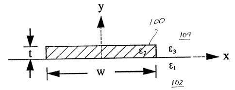
Figures 11a) and 1 (b) are a cross-sectional side view and a plan view,
respectively of a waveguide structure formed by a core comprising a lossy
metal film of thickness t, width w and permittivity E2. The metal film is
supported by a homogeneous semi-infinite substrate of permittivity E, and the
cover or superstrate is a homogeneous semi-infinite dielectric of permittivity
E3.
Figures 2(a) and 2(b) illustrate dispersion characteristics with thickness
of the first seven modes supported by such a metal film waveguide of width
w = 1 ,um. The ab and sb modes supported for the case w = oo are shown for
comparison. (a) Normalized phase constant. (b) Normalized attenuation
constant.
Figures 3(al,(b),(c) and (d) illustrate spatial distribution of the EY field
component related to the sse mode supported by such a metal film waveguide
of width w = 1 ,um for four film thicknesses. The waveguide cross-section is
located in the x-y plane and the metal region is outlined as the rectangular
dashed contour. The field distributions are normalized such that max; ~{EY} i
=
1.
Figures 4(a),(bl,(c) and (d) illustrate spatial distribution of the EY field
component related to two higher order modes supported by a metal film
waveguide of width w = 1 ,um for two film thicknesses. In all cases, the
waveguide cross-section is located in the x-y plane and the metal region is
outlined as the rectangular dashed contour. The field distributions are
normalized such that max;~t{EY}; = 1.
Figure 5 illustrates dispersion characteristics with thickness of the first
six modes supported by a metal film waveguide of width w = 1 ,um. The ab
and sb modes supported for the case w = ~ are shown for comparison. (a)
Normalized phase constant. (b) Normalized attenuation constant.
Figures 6(a1,(bl,(c) and (d) illustrate spatial distribution of the EY field
component related to modes supported by a metal film waveguide of width w
- 1 ,um. In all cases, the waveguide cross-section is located in the x-y plane
and the metal region is outlined as the rectangular dashed contour. The field
distributions are normalized such that max;~t{Ey}; = 1.
CA 02319949 2000-09-20
6
Figures 7(a) and 7(b) illustrate dispersion characteristics with thickness
of the first six modes supported by a metal film waveguide of width w = 0.5
,um. The ab and sb modes supported for the case w - ~ are shown for
comparison. (a) Normalized phase constant. (b) Normalized attenuation
constant.
Figures 8(a) and 8(b) illustrate dispersion characteristics with thickness
of the SSb and Sab modes supported by a metal film waveguide of width w
- 0.5 ,um for various cases of E3. (a) Normalized phase constant; the inset
shows an enlarged view of the region bounded by 0.04 <_ t <_ 0.08 ,um and
2.0 <_ ,Bl,Bo <_ 2.3. (b) Normalized attenuation constant; the inset shows an
enlarged view of the region bounded by 0.05 <- t <_ 0.08 ,um and 7.0 x 10⁻³
<- a/~o _< 2.0 x 10'2.
Figures 9(al,(b),(c) and (d) illustrate spatial distribution of the Ey field
component related to the sab' mode supported by a metal film waveguide of
width w = 0.5 ,um for four film thicknesses. The waveguide cross-section is
located in the x-y plane and the metal region is outlined as the rectangular
dashed contour. The field distributions are normalized such that max; ~t{EY} ;
_
1.
Figures 10(a),(b),(c) and (d) illustrate a contour plot of ~tf Sz} associated
with the long-ranging modes supported by metal film waveguides of width w
- 0.5 ,um and having different superstrate permittivities E3. In all cases,
the
outline of the metal film is shown as the rectangular dashed contour.
Figures 1 1 (a) and 11 (b) are a schematic front view and corresponding
top plan view of an electro-optic modulator employing the waveguide structure
of Figures 1 (a1 and 1 (b1.
Figures 12(a) and 12(b) are a schematic front view and corresponding
top view of an alternative electro-optic modulator;
Figure 12(c) illustrates an alternative connection arrangement of the
modulator of Figure 12(a);
Figure 13 is a schematic front view of a third embodiment of electro-
optic modulator;
Figure 14 is a schematic front view of a magneto-optic modulator;
Figure 15 is a schematic front view of a thermo-optic modulator;
Figure 16 is a schematic perspective view of an electro-optic switch;
Figure 17 is a schematic perspective view of a magneto-optic switch;
and
Figure 18 is a schematic perspective view of a thermo-optic switch.
CA 02319949 2000-09-20
7
BEST MODE(S~ FOR CARRYING OUT THE INVENTION:
The present invention is predicated upon a comprehensive investigation
of the purely bound modes of propagation supported by an important class of
asymmetric waveguiding structures comprising of a thin lossy metal film of
finite width, supported by a semi-infinite homogeneous dielectric substrate
and
covered by a different semi-infinite homogeneous dielectric superstrate.
Embodiments of the invention also rely upon an investigation of the evolution
of modes due to variations in the physical parameters of the waveguides.
In order to facilitate an understanding of the specific optical devices
embodying the invention, their theoretical basis will first be explained with
reference to Figures 1 to 10(d).
A. Description of the Waveguide Structure
Referring to Figure 1, the waveguide structure comprises a metal film
100 of thickness t, width w and equivalent permittivity E2, supported by a
semi-infinite homogeneous dielectric substrate 102 of permittivity E, and
covered by a semi-infinite homogeneous dielectric superstrate 104 of
permittivity e3. The Cartesian coordinate axes x and y used for the analysis
are
also shown; propagation takes place along the z axis, which is out of the
page.
It is assumed that the metal region shown in Figure 1 can be modeled
as an electron gas over the wavelengths of interest. According to classical or
Drude electron theory, the complex relative permittivity of the metal region
is
given by the well-known plasma frequency dispersion relation [3]:
z z
_ _ WP WP U
Er 2 1 WZ + UZ ] W / WZ + U2,
where cu is the excitation frequency, cv P is the electron plasma frequency
and
v is the effective electron collision frequency, often expressed as v=1 it
with
r defined as the relaxation time of electrons in the metal. When cv2 + v2 < cv
p2
(which is the case for many metals at optical wavelengths) a negative value
for the real part of e~,2 is obtained, implying that plasmon-polariton modes
can
be supported at interfaces with normal dielectrics.
B. Electromagnetic VIlave and Field Equations
The modes supported by the structure illustrated in Figure 1 are obtained
by solving a suitably defined boundary value problem based on Maxwell's
equations written in the frequency domain for a lossy inhomogeneous isotropic
CA 02319949 2000-09-20
medium. Uncoupling Maxwell's equations yields the following time-harmonic
vectorial wave equations for the E and H fields:
v x v x E-w2 s (x, y) ~ E = o (2)
v x E-' (x, y) vxH-c.~2~,H = o (3)
where the permittivity E is a complex function of cross-sectional space,
describing the waveguide structure. For the structures analyzed in this
specification,,u is homogeneous and taken as the permeability of free
space,uo.
The above serve as the physical basis for the analysis of the structures of
interest.
The boundary value problem is solved numerically by applying the
Method of Lines (MoL). The MoL is a well-known numerical technique and its
application to various electromagnetic problems, including optical
waveguiding,
is well-established [12]. The MoL is rigorous, accurate and flexible. It can
handle a wide variety of waveguide geometries, including the structures at
hand. The method is not known to generate spurious or non-physical modes.
Except for a 1-D spatial discretization (applied along the x direction in this
case), the method is exact. The MoL formulation used in this study is detailed
in [13], and its application to the modelling of waveguiding structures such
as
those of concern in this specification is summarized in [10]; the formulation
will
therefore not be repeated here.
The MoL generates mode solutions that satisfy Equations (2) and (3).
Since the structures under consideration are invariant along the propagation
axis (taken to be in the +z direction), the mode fields vary along this
dimension
according to e-'~ where y = a+j,8 is the complex propagation constant of the
mode, a being its attenuation constant and ,B its phase constant. The spatial
distribution of all six field components related to a mode can also be
generated
by the MoL over the 2-D cross-section of the structure if they are desired.
The physical symmetry of the structure along the center vertical axis is
exploited to increase the accuracy of the results and to reduce the numerical
effort required to generate the mode solutions. This is achieved by placing
either an electric wall (Ete" _ ~) or a magnetic wall (Hta~ _ ~) boundary
condition along the y axis shown in Figure 1.The top and bottom boundary
conditions are placed at infinity and the remaining lateral boundary condition
is either placed far enough from the guide to have a negligible effect on the
mode calculation, or a lateral absorbing boundary condition is used to
simulate
infinite space, depending on the level of confinement observed in the
resulting
mode.
CA 02319949 2000-09-20
9
As discussed in reference [10], the propagation constant of a mode
computed using the method of lines converges in a monotonic or smooth
manner with a reduction in the discretization interval, which means that it is
sensible to apply an extrapolation technique to generate more accurate values
for the propagation constant (14]. The convergence of the computed
propagation constants has been monitored and extrapolated values obtained
using Richardson's extrapolation formula [15], were used to generate most of
the graphs in the attached drawings.
C. Modes Supported by Metal Film Slab Waveguides
In general, only two purely bound TM surface modes, each having three
field components, are guided by an infinitely wide metal film waveguide [5].
In
the plane perpendicular to the direction of wave propagation, the electric
field
of the modes comprises a single component, normal to the interfaces and
having either a symmetric or asymmetric spatial distribution across the
waveguide. The symmetric mode can have a small attenuation constant and is
often termed a long-range surface plasmon-polariton. The fields related to the
asymmetric mode penetrate more into the metal than the fields associated with
the symmetric mode and are usually much lossier by comparison. In addition
to purely bound modes, leaky modes are also known to be supported by these
structures.
In the symmetric metal slab structure (similar to Figure 1 but w = ~ and
E3 - E,) the spatial distribution of the mode fields is truly symmetric or
asymmetric about the horizontal axis passing through the center of the metal
film; that is, the fields can be generated by placing an electric wall of
symmetry
along this axis. In this structure, the loss associated with the asymmetric
mode
increases with decreasing film thickness as the fields penetrate progressively
deeper into the lossy metal. In the case of the symmetric mode, the
attenuation
decreases with decreasing film thickness, as the mode evolves towards the
TEM (Transverse ElectroMagnetic) wave supported by the background. There
is no cutoff thickness for either mode in this structure. As the thickness of
the
film increases, both the symmetric and asymmetric modes become degenerate,
their propagation constants converging to that of a plasmon-polariton mode
supported by the interface between semi-infinite metallic and dielectric
regions,
which is given via the following equations[5]:
Er~l~r~2
Er,1 + ~r,2
a
CA 02319949 2000-09-20
a/~3o + _~ Er,l~r~2 (51
~r,l + Er,2
5 where ,Bo = cv/co with co being the velocity of light in free space, and
E~,, and
E~,2 are the complex relative permittivities of the materials.
In the asymmetric metal slab structure (like that shown in Figure 1 but
w = ~ and E3 ~ E,), the spatial distribution of the mode fields is not truly
symmetric or asymmetric about the center horizontal axis. Rather, the
10 distributions are symmetric-like or asymmetric-like; that is the
distributions have
the general form of those found in the symmetric structure but the fields are
localized near one of the interfaces. The modes however are still called
symmetric and asymmetric modes. The symmetric mode field distribution has
a maximum at the interface with the dielectric of lowest permittivity while
the
asymmetric mode has a maximum at the interface with the dielectric of highest
permittivity. The loss associated with the asymmetric mode increases with
decreasing film thickness and this mode does not have a cut-off thickness. The
loss associated with the symmetric mode decreases with decreasing film
thickness and a cut-off thickness for the mode exists; that is, the mode is
not
supported for films of thickness less than a cut-off value. It is reasonable
that
a cut-off thickness for the symmetric mode exists in an asymmetric structure
since the mode cannot evolve into a TEM wave supported by the background
as t ~ 0. The background comprises the interface between semi-infinite
dielectric media and such an interface cannot support a TEM mode. As the
thickness of the metal film increases, the modes of the asymmetric structure
evolve into uncoupled plasmon-polariton modes supported by the isolated top
and bottom interfaces. The propagation constant of the mode localized at the
bottom interface converges to the value given by Equations (4) and (5) and the
propagation constant of the mode localized at the top interface is given by
these same equations by substituting E, with E3.
The widely accepted nomenclature for identifying the modes of infinitely
wide structures consists in using the letters a or s for asymmetric or
symmetric
transverse field distributions, respectively, followed by a subscript b or I
for
bound or leaky modes, respectively. This nomenclature is used for the modes
of symmetric as well as asymmetric metal slab structures.
D. Modes Supported by Symmetric Structures Constructed From Metal Films
of Finite Width.
CA 02319949 2000-09-20
11
The purely bound modes supported by a thin lossy metal film of finite
width, embedded in an infinite homogeneous dielectric (E3 = E~ in Figure 1 )
have recently been characterized [10] and [38]. Only the features of these
modes that are relevant to the current study are summarized here; a complete
description and a discussion of the modes can be found in [10] and [38].
The modes supported by a symmetric structure are not TM in nature but
if the structure has an aspect ratio wlt > 1, then the Ey field component
dominates. The modes can be divided into four families depending on the
symmetry of their fields. Four symmetries, corresponding to the four possible
combinations of electric and magnetic walls placed along the center horizontal
and vertical axes, exist and define the families. A mode nomenclature, based
on the one used to identify modes in metal slab waveguides, describes the
spatial distribution of the main transverse electric field component, which is
the
Ey component in most structures of practical interest. A pair of letters a or
s
identify whether the main transverse electric field component is asymmetric or
symmetric with respect to the y and x axes, respectively. A superscript is
then
used to track the number of extrema observed in the spatial distribution of
this
field component along the largest dimension (usually along the x axis) between
the corners. A second superscript n could be added to track the extrema along
the other dimension (the y axis) if modes exhibiting them are found. Finally,
a
subscript b or / is used to identify whether the mode is bound or leaky. Leaky
modes are known to exist in metal film slab structures and it is envisaged
that
they will exist in metal films of finite width.
The ssb, sab, asb and aab modes are the first modes supported (one for
each of the four possible quarter-symmetries) and thus may be considered as
the fundamental modes. In addition to the four fundamental modes, higher
order modes having additional variations in the spatial distribution of their
mode
fields are supported.
The dispersion of all modes with film thickness is in general consistent
with the behaviour observed for the purely bound modes supported by the
metal film slab waveguide. In addition, one of the fundamental modes and
some higher order modes have cut-off thicknesses. The higher order modes
have a cut-off width, below which they are no longer propagated. The effect
on the modes of varying the background permittivity is consistent with the
general behaviour observed for the modes supported by a metal film slab
waveguide. In addition, the cut-off width of the higher order modes decreases
with decreasing background permittivity while all cut-off thicknesses
increase.
CA 02319949 2000-09-20
12
One of the fundamental modes supported by the symmetric structure,
the Ssb mode exhibits very interesting characteristics and is potentially
quite
useful. This mode evolves with decreasing film thickness towards the TEM
wave supported by the background, (an evolution similar to that exhibited by
the sb mode in metal film slab waveguidesl, its losses and phase constant
tending asymptotically towards those of the TEM wave. In addition, decreasing
the film width reduces the losses below those of the sb mode supported by the
corresponding metal film slab waveguide. Reducing the background permittivity
further reduces the losses. However, a reduction in losses is always
accompanied by a reduction in field confinement to the waveguide core which
means that attenuation and confinement must be traded-off one against the
other. The mode evolved into its most useful form has a field distribution
that
renders it excitable using end-fire techniques [16]. In reference [17], the
present inventor et al. disclosed that plasmon-polariton waves supported by
thin metal films of finite width have recently been observed experimentally at
optical communications wavelengths using this method of excitation [17].
III. Mode Characteristics and Evolution With Film Thickness: Small Asymmetry
A. Mode Solutions for a Metal Film Slab Waveguide
The study begins with the reproduction of results for an infinitely wide
asymmetric metal film waveguide (similar to that shown in Figure 1 but with
w = ~), taken from the standard work on such structures [51. In order to
remain consistent with their results, the optical free-space wavelength of
excitation is set to ~lo = 0.633 ,um and their value for the relative
permittivity
of the silver film at this wavelength is used: E,,2 = -19 - j0.53. The
relative
permittivity of the bottom and top dielectric regions are set to E,,~ = 4 (n,
= 2)
and E~,3 = 3.61 (n3 = 1.9); these values create a structure having a small
asymmetry with respect to the horizontal dimension.
The dispersion curves of the sb and ab modes supported by the infinitely
wide structure were computed using the MoL and the results are shown in
Figure 2. From this figure, it is seen that the propagation constant of the ab
mode tends towards that of the plasmon-polariton mode supported by the
bottom interface, given by Equations (4) and (5), as the thickness of the film
increases. It is also noted that this mode does not exhibit a cutoff thickness
while it is clear that the sb mode has one near t = 18 nm. The propagation
constant of the sb mode is seen to tend towards the value of a plasmon-
polariton mode supported by the top interface as the thickness increases.
These results are in perfect agreement with those reported in [5].
CA 02319949 2000-09-20
13
B. Modes Supported by a Metal Film of Width w = 7 ,um
The study proceeds with the analysis of the structure shown in Figure
1 for the case w = 1 ,um. The material parameters and free-space wavelength
that were used in the previous case w - oo were also used here. The
dispersion curves for the first seven modes were computed using the MoL and
the results are shown in Figure 2.
In this asymmetric structure, true field symmetry exists only with respect
to the y axis. With respect to the horizontal dimension, the modes have a
symmetric-like or asymmetric-like field distribution with field localization
along
either the bottom or top metal-dielectric interface. The modes that have a
symmetric-like distribution with respect to the horizontal dimension are
localized along the metal-dielectric interface with the lowest dielectric
constant,
while modes that have an asymmetric-like distribution with respect to this
axis
are localized along the metal-dielectric interface with the highest dielectric
constant. This behaviour is consistent with that observed for asymmetric metal
slab waveguides.
The mode nomenclature adopted for symmetric structures [10] can be
used without ambiguity to describe the modes supported by asymmetric
structures as long as the modes are identified when the metal film is fairly
thick, before significant coupling begins to occur through the metal film, and
while the origin of the mode can be identified unambiguously. As the metal
film
thickness decreases, the modes (and their fields) can evolve and change
considerably more in an asymmetric structure compared to a symmetric one.
The number of extrema in the main transverse electric field component of the
mode is counted along the lateral dimension at the interface where the fields
are localized. This number is then used in the mode nomenclature.
It was observed in [10) that the modes supported by a metal film of
finite width are in fact supermodes created from a coupling of "edge" and
"corner" modes supported by each metal-dielectric interface defining the
structure. As the thickness and width of the metal decrease, the coupling
between these interface modes intensifies leading to dispersion and possibly
evolution of the supermode. In asymmetric structures, the bound modes are
also supermodes created in a similar manner, except that dissimilar interface
modes may couple to each other to create the supermode. For instance, a
mode having one field extremum along the top interface (along the top edge
bounded by the corners) may couple with a mode having three extrema along
the bottom interface. The main selection criterion determining which interface
modes will couple to create the supermode is a similarity in the value of
their
CA 02319949 2000-09-20
14
propagation constants. For all modes supported by an asymmetric structure,
an apparent symmetry or asymmetry with respect to the horizontal dimension
can still be observed in the corner modes.
The sa6, aab, ssb and asb modes are the fundamental modes
supported by the structure. The sab and aab modes are comprised of coupled
corner modes, resembling the corresponding modes in a symmetric structure
[10], except that the fields are localized near the substrate. These two modes
do not change in character as the thickness of the film decreases. A narrowing
of the metal film would eventually break the degeneracy observed in Figure 2.
For a sufficiently large thickness (about 100 nm for the present
structure), the ssb and asb modes are comprised of coupled corner modes
much like the corresponding modes in a symmetric structure except that the
fields are localized near the superstrate. As the thickness of the metal film
decreases, both of these modes begin to evolve, changing completely in
character for very thin films. Figures 3(a) to 3(d) show the evolution of the
EY
field component related to the ssb mode as the thickness of the film ranges
from 100 nm (Figure 3(a) to 40 nm (Figure 3(d1). It is clearly seen that the
mode evolves from a symmetric-like mode having fields localized near the
superstrate to an asymmetric-like mode having fields localized along the
substrate-metal interface. A similar evolution is observed for the asb mode.
This change in character is also apparent in their dispersion curves: they
follow
the general behaviour of a symmetric-like mode for large thicknesses but then
slowly change to follow the behaviour of an asymmetric-like mode as the
thickness decreases. Since the substrate dielectric constant is larger than
the
superstrate dielectric constant, the mode is "pulled" from a symmetric-like
mode to an asymmetric-like mode (having field localization at the substrate-
metal interface) as the metal film becomes thinner.
Figures 4(a) to 4(d) show the Ey field component related to
the ssb and sab modes for two film thicknesses. From this figure it is noted
that the top and bottom edge modes comprising a supermode are different
from each other. In part (a) for instance, it is seen that the bottom edge
mode
has three extrema and is of higher order than the top edge mode which has one
extremum. A similar observation holds for part (c) where it can be seen that
the
bottom edge mode has one extremum while the top one has none. In this
structure, the substrate has a higher dielectric constant than the superstrate
so
the phase constant of a particular substrate-metal interface mode will be
higher
than the phase constant of the same mode at the metal-superstrate interface.
Since a supermode is created from a coupling of edge modes having similar
CA 02319949 2000-09-20
propagation constants, it should be expected that in an asymmetric structure
different edge modes may couple to create a supermode. Higher-order modes
have in general smaller values of phase constant compared to lower-order
modes, so in structures having E3 < E~, all supermodes are comprised of a
5 bottom edge mode of the same order or higher than the top edge mode, as
shown in Figure 4. If E3 > E~, then the opposite statement is true.
A careful inspection of the fields associated with
the ssb, sab and aab modes reveals that as the thickness of the film
decreases, the mode fields may evolve in a smooth manner similar to that
10 shown in Figure 3, but in addition a change or "switch" of the constituent
edge modes may also occur. For instance, from Figure 4(c), the sab mode is
seen to comprise a substrate-metal interface mode having one extremum for
a film thickness of 100 nm, while for a thickness of 60 nm the substrate-metal
interface mode has three extrema, as shown in Figure 4(dl. Since higher-order
15 modes have in general lower phase constants than lower-order modes, this
change in edge modes causes a reduction in the phase constant of
the sab mode in the neighbourhood of 60 nm, as shown in Figure 2 (a).
Another change occurs near 40 nm as the corner modes switch from being
symmetric-like (as in Figures 4(c) and 4(d~) to being asymmetric-like with
respect to the horizontal dimension. This change is again reflected in the
dispersion curve of the sab mode as its phase constant is seen to increase
with a further decrease in thickness. In general, the changes in the edge and
corner modes are consistent with the directions taken by the dispersion curves
as the film thickness decreases, thus explaining the oscillations in the
curves
seen in Figure 2.
The only potentially long-ranging mode supported by this structure at the
wavelength of analysis is the sse mode. As shown in Figure 2, the mode has
a cutoff thickness near t = 22 nm and though the attenuation drops quickly
near this thickness, it should be remembered that the field confinement does
so as well. Furthermore, the spatial distribution of the main transverse field
component related to this mode evolves with decreasing thickness in the
manner shown in Figure 4(al and 4(b1, such that near cutoff the spatial
distribution has strong extrema along the top and bottom edges. These extrema
render the mode less excitable using an end-fire technique so coupling losses
would be higher compared to the fundamental symmetric mode in symmetric
waveguides. Also, the fact that the mode would be operated near its cutoff
thickness implies that very tight tolerances are required in the fabrication
of
CA 02319949 2000-09-20
16
structures. Nevertheless, it should be possible to observe propagation of this
mode in a suitable structure using an end-fire experiment (16,17].
IV. Mode Characteristics and Evolution With Film Thickness: Large Asymmetry
A. Mode Solutions for a Metal Film Slab Waveguide
The study proceeds with the analysis of structures having a large
difference in the dielectric constants of the substrate and superstrate. With
respect to Figure 1, the relative permittivities of the substrate and
superstrate
are set to E~,, = 4 (n, = 2) and E~,3 = 2.25 (n3 = 1.5), respectively, the
width
of the metal film is set to w = oo, and the dielectric constant of the metal
region and the wavelength of analysis are set to the same values as in Section
III. The dispersion curves of the sb and ab modes supported by this structure
can be seen in Figure 5. Comparing with Figure 2, it is observed that the sb
mode has a larger cutoff thickness in a structure having a large asymmetry
than in a structure having similar substrate and superstrate dielectric
constants.
The results shown were computed using the MoL and are in perfect agreement
with those reported in (5].
B. Modes Supported by a Metal Film of Width w = 1 ,um
The structure shown in Figure 1 was analyzed using the MoL for w =
1 ,um and for the same material parameters and free-space wavelength as those
given above for w = ~. The dispersion curves of the first six modes supported
by the structure are shown in Figure 5.
An inspection of the mode fields related to the sab and aab modes
reveals that these modes are again comprised of coupled corner modes with
fields localized at the substrate-metal interface. The modes do not change in
character as the thickness of the film decreases and a narrowing of the metal
film would eventually break the degeneracy observed in Figure 5.
The spatial distribution of the Ey field component related to
the, ssb, asb, sab and aab modes is given in Figure 6. It is noted from this
figure that in all cases the metal-superstrate interface modes are similar:
they
have fields with no extrema along the interface but rather that are localized
near the corners and have either a symmetric or asymmetric distribution with
respect to the y axis. These corner modes are in fact the lowest order modes
supported by the metal-superstrate interface; they have the largest value of
phase constant and thus are most likely to couple with edge modes supported
by the substrate-metal interface to form a supermode. From Figures 61a) and
6(b) it is observed that the substrate-metal interface modes comprising
CA 02319949 2000-09-20
17
the Ssb and asb modes are of very high order. This is expected since the
substrate dielectric constant is significantly higher than the superstrate
dielectric constant and higher order modes have lower values of phase
constant. The Ssb and asb modes shown in Figures 61a) and 6(b) indeed have
fields that are localized along the metal-superstrate interface, while
the Sab and aab modes shown in Figures 6 (c) and 6(d) have fields that are
localized along the substrate-metal interface.
One effect caused by increasing the difference between the substrate
and superstrate dielectric constants, is that the difference between the
orders
of the top and bottom edge modes comprising a supermode can increase. This
effect can be observed by comparing Figure 3(a) with Figure 6(a). In the
former, there is no difference between the orders of the top and bottom edge
modes, while in the latter the difference in the orders is 5. Another effect
is
that the degree of field localization increases near the interface between the
metal and the dielectric of higher permittivity, for all modes that are
asymmetric-like with respect to the horizontal dimension. This effect can be
seen by comparing the fields related to the Sab mode shown in Figures 6(c)
and 4(c1. A comparison of the fields related to the Sab and aab modes reveals
that this effect is present in these modes as well.
From the dispersion curves shown in Figure 5(a), it is apparent that the
normalized phase constant of all modes converge with increasing film thickness
to normalized phase constants in the neighbourhood of those supported by
plasmon-polariton waves localized along the associated isolated edge. The
normalized phase constant of modes having fields localized at the substrate-
metal interface, converge with increasing film thickness to normalized phase
constants in the neighbourhood of that related to the ab mode, while the
normalized phase constant of modes having fields localized along the metal-
superstrate interface converge to values near that of the sb mode. This
behaviour is present though less apparent in structures where the asymmetry
is smaller, such as the one analyzed in Section III.
By comparing Figures 2 and 5, it is noted that the dispersion curves of
the modes are much smoother when the difference in the substrate and
superstrate dielectric constants is large. This is due to the fact that the
edge
modes comprising the supermodes are less likely to change or switch as they
do in a structure having similar substrate and superstrate dielectric
constants.
Thus modes that start out being symmetric-like with respect to the horizontal
dimension remain so as the thickness of the film decreases. The cutoff
' CA 02319949 2000-09-20
18
thickness of the symmetric-like modes also increases as the difference between
the substrate and superstrate dielectric constants increases.
It is apparent that introducing a large asymmetry can hamper the ability
of the structure to support useful long-ranging modes. Any mode that is long
s ranging would likely have fields with numerous extrema along the width of
the
interface between the metal film and the dielectric of higher permittivity, as
shown in Figures 61a) and 6(b1.
V. Mode Dispersion with Film Width: Small Asymmetry
An asymmetric structure comprising the same dielectrics as the
structures studied in Section III, but having a metal film of width w = 0.5 Nm
was analyzed at the same free-space wavelength in order to determine the
impact of a narrowing film width on the modes supported. The structure was
analyzed using the MoL and Figure 7 gives the dispersion curves obtained for
the first few modes supported.
Comparing Figure 7 with Figure 2 reveals that reducing the width of the
film does not cause major changes in the behaviour of the fundamental modes,
but does have a major impact on the higher order modes. It is noted that
reducing the film width increases the cutoff thickness of the Ssb mode. This
higher order mode is symmetric-like with respect to the horizontal dimension,
and the cutoff thickness of the symmetric-like modes in general increases as
the width of the film decreases due to a reduction in field confinement to the
metal film. The aab mode was sought but not found for this film width.
It is also noted by comparing Figures 7 and 2 that the Sab mode evolves
quite differently depending on the width of the film. For a film width of w =
1 ,um, the mode follows the general behaviour of an asymmetric-like mode
whereas for a film width of w = 0.5,um, the mode evolves as a symmetric-like
mode, and has a cutoff thickness near t = 27 nm. When the film is wide, it
becomes possible for numerous higher order edge modes (having similar values
of phase constant) to be supported by the substrate-metal or metal-superstrate
interfaces, so edge modes comprising a supermode are likely to change or
switch as the thickness of the film is reduced as shown in Figures 4(c) and
4(d). For a narrow metal film, some of the higher order edge modes may be
cutoff thus rendering changes in edge modes impossible. In such a case, the
supermode may be forced to evolve in a smooth manner with decreasing film
thickness. A close inspection of the mode fields related to the Sab mode for
a film width of w = 0.5 ,um reveals that there are no changes to the edge
modes as the thickness decreases, rather the mode evolves smoothly from its
CA 02319949 2000-09-20
19
field distribution at a large thickness (similar to that shown in Figure 4
(c)) to
having a symmetric-like distribution with only one extremum along the top and
bottom edges of the film. A change in behaviour due to a change in the width
of the metal film was observed only for the Sab mode in this study, but such
changes are in general not limited to this mode.
The Sab and Ssb modes could be made to propagate over useful
distances in this structure, if they are excited near their cutoff
thicknesses.
However, the difficulties outlined in Section III B regarding the excitation
of
modes near cutoff also hold here.
VI. Evolution of the Ssb and Sati Modes With Structure Asymmetry
The SSb and Sab modes are of practical interest. The Ssb mode is the
main long-ranging mode supported by symmetric finite-width metal film
structures, and as demonstrated in the previous section, the Sab mode can be
the main long-ranging mode supported by asymmetric finite-width structures.
In metal films of the right thickness, they are also the modes that are the
most
suitable to excitation in an end-fire arrangement.
Structures comprising a substrate dielectric having n, = 2, of a metal
film of width w = 0.5 ,um, and of various superstrate dielectrics having n3 =
2, 1.99, 1.95 and 1.9 were analyzed at the same free-space wavelength as in
Section III. The equivalent permittivity of the metal film was also set to the
same value as in Section III. These analyses were performed in order to
investigate the effects on the propagation characteristics of
the Ssb and Sab modes caused by a slight decrease in the superstrate
permittivity relative to the substrate permittivity. Figure 8 shows the
dispersion
curves with film thickness, obtained for these modes in the four structures of
interest.
As seen in Figure 8(a) and its inset, the dispersion curves of the modes
intersect at a certain film thickness only for the symmetric case (n3 = n~).
As
soon as some degree of asymmetry exists, the curves no longer intersect,
though they may come quite close to each other if the asymmetry is small, as
seen in the case of n3 = 1.99. As the degree of asymmetry increases, the
separation between the curves increases.
The evolution with film thickness of the Sab mode is shown in Figure
9 for the case n3 = 1.99 and for thicknesses about t = 59 nm (near the
maximum in its phase dispersion curve). The evolution of this mode for the
cases n3 = 1.95 and 1.9 is similar to that shown. The evolution with film
thickness of the SSb mode is similar in these structures to the evolution
shown
CA 02319949 2000-09-20
in Figure 3 for the case w = 1 ,um and n3 = 1.9. Comparing Figures 9 and 3,
reveals that the modes "swap" character near t = 59 nm. For film thicknesses
sufficiently above this value, the modes exhibit their defining character as
shown in Figures 3(a) and 9(a), but for film thicknesses below it, each mode
5 exhibits the other's character, as shown in Figures 3(d) and 9(d). This
character
swap is present for the three cases of asymmetry considered here (n3 =1.99,
1.95 and 1.9) and explains the behaviour of the dispersion curves shown in
Figure 8.
From Figure 8, it is noted that a cutoff thickness exists for the long-
10 ranging mode as soon as an asymmetry is present in the structure. It is
also
observed that the cutoff thickness increases with increasing asymmetry. In the
case of n3 = 1.99, the cutoff thickness of the mode is near t = 12 nm, while
for n3 = 1.9 the cutoff thickness is near t = 27 nm. As the width of the metal
film w increases, the cutoff thickness of the Sab mode decreases as long as
15 the mode remains long-ranging (recall that the character of this mode may
also
change with film width such that its behaviour is similar to the ab mode in
the
corresponding slab structure, as shown in Figure 2). Also, it is clear from
Figure
7 that the cutoff thickness of the Sab mode is greater than the cutoff
thickness of the sb mode supported by the corresponding slab structure. These
20 results imply that the long-ranging mode supported by a thin narrow metal
film
is more sensitive to differences in the superstrate and substrate
permittivities
than the sb mode supported by the corresponding slab structure. This is
reasonable in light of the fact that in finite-width structures the mode
fields
tunnel through the metal as in slab structures, but in addition the fields
also
wrap around the metal film.
Figure 8~b) shows that near cutoff, the attenuation of the Sab mode
supported by an asymmetric structure drops much more rapidly than the
attenuation of the Ssb mode supported by a symmetric structure. Thus a
means for range extension, similar to that observed in asymmetric slab
structures [6], exists for metal films of finite width, though the
difficulties
related to the excitation of a mode near its cutoff thickness as described in
Section III B also apply here.
Figures 10(a) to 10(d) show contour plots of ~?{SZ} associated with the
long-ranging modes for the four cases of superstrate permittivity considered.
SZ is the z-directed component of the Poynting vector and its spatial
distribution
is computed from the spatial distribution of the mode fields using:
SZ = ( Ely' - E~Ix~ ) / 2 ( 6 )
CA 02319949 2000-09-20
21
where Hxy denotes the complex conjugate of Hx,y. Figure 10(a) shows the
contour plot associated with the Ssb mode supported by a symmetric
structure (n3 = n~ = 2) of thickness t = 20 nm. Figures 10(b),(c) and (d) show
contours associated with the Sab mode for the three cases of structure
asymmetry considered. The contour plots shown in Figures 10(b),(c) and (d)
are computed for film thicknesses slightly above cutoff, representative of the
thicknesses that would be used to observe these long-ranging modes
experimentally. From this figure, it is noted that the contour plots become
increasingly distorted and the fields increasingly localized at the metal-
superstrate interface as the degree of asymmetry in the structure increases.
It
is also apparent by comparing Figures 10(a) and 10(d) that in an end-fire
experiment, less power should be coupled into the Sab mode supported by the
asymmetric structure with n3 = 1.9, compared to the Ssb mode supported by
the symmetric structure. End-fire coupling losses seem to increase with
increasing structure asymmetry.
The high sensitivity of the long-ranging mode supported by thin metal
films of finite width, to structure asymmetry is potentially useful. A small
induced asymmetry (created via an electro-optic effect present in the
dielectrics
say) can evidently effect a large change in the propagation characteristics of
the long-ranging mode. From Figure 8, it is apparent that a difference between
the substrate and superstrate refractive indices as small as n, - n3 = ~n =
0.01 is sufficient to create an asymmetric structure where the long-ranging
mode has a cutoff thickness of about t = 12 nm. From Figure 8la), a slightly
larger difference of ~n = 0.05 changes the normalized phase constant of the
long-ranging mode by 0(,8/,Bo) ~ 0.025 for a metal film thickness of t = 20
nm.
Both of these effects are potentially useful.
VII. Conclusion
The long-ranging modes supported by asymmetric structures of finite
width have a rapidly diminishing attenuation near their cutoff thickness (like
asymmetric slab structures). The rate of decrease of the attenuation with
decreasing thickness near cutoff is greater than the rate related to
the SSb mode in symmetric structures. However field confinement also
diminishes rapidly near cutoff, implying that the structures ought to be
fabricated to very tight tolerances and that all metal-dielectric interfaces
should
be of the highest quality. It has also been found that decreasing the width of
the film increases the cutoff thickness of the main long-ranging mode. Below
this cutoff thickness no purely bound long-ranging mode exists. The long-
CA 02319949 2000-09-20
22
ranging mode supported by metal films of finite-width are thus more sensitive
to the asymmetry in the structure compared to the sb mode supported by
similar slab waveguides. This is a potentially useful result in that a small
induced change in substrate or superstrate refractive index can have a greater
impact on the long-ranging mode supported by a finite-width structure
compared to a similar slab waveguide.
Specific Embodiments of modulation and switching devices
Modulation and switching devices will now be described which make use
of the fact that an asymmetry induced in optical waveguiding structures having
as a guiding element a thin narrow metal film may inhibit propagation of the
main long-ranging purely bound plasmon-polariton mode supported.
The asymmetry in the structure can be in the dielectrics surrounding the
metal film. In this case the permittivity, permeability or the dimensions of
the
dielectrics surrounding the strip can be different. A noteworthy case is where
the dielectrics above and below the metal strip have different permittivities,
in
a manner similar to that shown in Figure 1.
A dielectric material exhibiting an electro-optic, magneto-optic, thermo
optic, or piezo-optic effect can be used as the surrounding dielectric medium.
The modulation and switching devices make use of an external stimulus to
induce or enhance the asymmetry in the dielectrics of the structure.
Figure 1 1 depicts an electro-optic modulator comprising two metal strips
1 10 and 112 surrounded by a dielectric 114 exhibiting an electro-optic
effect.
Such a dielectric has a permittivity that varies with the strength of an
applied
electric field. The effect can be first order in the electric field, in which
case it
is termed the Pockets effect, or second order in the electric field (Kerr
effect),
or higher order. Figure 11 (a) shows the structure in cross-sectional view and
Figure 11 (b) shows the structure in top view.
The bottom metal strip 110 and the surrounding dielectric 1 14 form the
optical waveguide. The bottom metal strip 110 is dimensioned such that a
purely bound long-ranging plasmon-polariton wave is guided by the structure
at the optical wavelength of interest. Since the guiding strip 1 10 is
comprises
a metal, it is also used as an electrode and is connected to a voltage source
116 via a minimally invasive electrical contact 118 as shown. The second
metal strip 112 is positioned above the first at a distance large enough that
optical coupling between the strips is negligible. It is noted that the second
strip could also be placed below the waveguiding strip instead of above. The
second strip acts as a second electrode.
CA 02319949 2000-09-20
23
The intensity of the optical signal output from the waveguide can be
varied or modulated by varying the intensity of the voltage V applied by the
source 116. When no voltage is applied, the waveguiding structure is
symmetric and it supports a plasmon-polariton wave. When a voltage is
applied, an asymmetry in the waveguiding structure is induced via the electro-
optic effect present in the dielectric 14 and the propagation of the plasmon-
polariton wave is inhibited. The degree of asymmetry induced may be large
enough to completely cut-off the main purely bound long-ranging mode thus
enabling a very high modulation depth to be achieved.
Figures 12(a) and 2(b) show an alternative design for an electro-optic
modulator which is similar to that shown in Figure 1 1 (a) but comprising
electrodes 112A and 1128 placed above and below, respectively, the metal
film 1 10 of the optical waveguide. Figure 121a) shows the structure in cross-
sectional view and Figure 12(b) shows the structure in top view. A first
voltage
source 116A connected to the metal film 110 and the upper electrode 112A
applies a first voltage V, between them. A second voltage source 112B
connected to metal film 110 and lower electrode 112B applies a voltage V2
between them. The voltages V~ and V2, which are variable, produce electric
fields E~ and E2 in portions 114A and 1148 of the dielectric material. The
dielectric material used exhibits an electro-optic effect. The waveguide
structure shown in Figure 12(cl is similar in construction to that shown in
Figure 12(a) but only one voltage source 116C is used. The positive terminal
( + ) of the voltage source 116C is shown connected to metal film 110 while
its negative terminal (-) is shown connected to both the upper electrode 112A
and the loser electrode 112B. With this configuration, the electric fields E,
and
E2 produced in the dielectric portions 114A and 114B, respectively, are in
opposite directions.
Thus, in the waveguide structure of Figure 12(a), selecting appropriate
values for the voltages V~ and V2 induces the desired asymmetry. In the
waveguide structure of Figure 12(c), the asymmetry is induced by the relative
direction of the electric field above and below the waveguiding strip 110
since
the voltage V applies to the electrodes 112A and 112B produces electric fields
acting in opposite directions in the portions 114A and 114B of the dielectric
material.
The structures shown in Figures 12(a),(b) and (c) can operate to very
high frequencies since a microwave transmission line is in effect created by
the
three metals (stripline).
CA 02319949 2000-09-20
24
Figure 13 shows in cross-sectional view yet another design for an
electro-optic modulator. In this case, the metal film 110 is embedded in the
middle of dielectric slab 114 with first portion 114D above it and second
portion 1 14E below it. Electrodes 112D and 112E are placed laterally along
the
edges of the upper portion 114D of the dielectric 1 14 as shown and connected
to voltage source 116E which applies voltage to them to induce the desired
asymmetry in the structure. Alternatively, the electrodes 1 12D, 112E could be
placed laterally along the bottom portion 114E of the dielectric 114, the
distinct portions of the dielectric material still being above and below the
strip.
Figure 14 shows an example of a magneto-optic modulator where the
waveguiding strip 110 and overlying electrode 112F are used to carry a current
/ in the opposite directions shown. The dielectric material surrounding the
metal
waveguide 110 exhibits a magneto-optic effect. The magnetic fields generated
by the current / add in the dielectric portion between the electrodes 110 and
112F and essentially cancel in the portions above the top electrode 1 12F and
below the waveguide 110. The applied magnetic field thus induces the desired
asymmetry in the waveguiding structure.
Figure 15 depicts a thermo-optic modulator wherein the waveguiding
strip 1 10 and the overlying electrode 1 12G are maintained at temperatures TZ
and T~ respectively. The dielectric material 114 surrounding the metal
waveguide exhibits a thermo-optic effect. The temperature difference creates
a thermal gradient in the dielectric portion 1146 between the electrodes. The
applied temperatures thus induce the desired asymmetry in the waveguiding
structure.
It should be appreciated that the modulator devices described above with
references to Figures 11 (a) to 15 may also serve as variable optical
attenuators
with the attenuation being controlled via the external stimulus, i.e. voltage,
current, temperature, which varies the electromagnetic property.
Figures 16, 17 and 18 depict optical switches that operate on the
principle of "split and attenuate". In each case the input optical signal is
first
split into N outputs using a power divider; a one-to-two power split being
shown in Figures 16, 17 and 18. The undesired outputs are then "switched
off" or highly attenuated by inducing a large asymmetry in the corresponding
output waveguides. The asymmetry must be large enough to completely cut-off
the main purely bound long-ranging mode supported by the waveguides. The
asymmetry is induced by means of overlaying electrodes as in waveguide
structures of Figures 11, 14 or 15, respectively. In the switches shown in
Figures 16, 17 and 18, the basic waveguide configuration is the same and
CA 02319949 2000-09-20
comprises an input waveguide section 120 coupled to two parallel branch
sections 122A and 1228 by a wedge-shaped splitter 124. All four sections
120, 122A, 1228 and 124 are co-planar and embedded in dielectric material
126. The thickness of the metal film is d3. Two rectangular electrodes 128A
5 and 1288, each of thickness d~, are disposed above branch sections 122A and
1228, respectively, and space form them by a thickness d2 of the dielectric
material 126. Each of the electrodes 128A and 1288 is wider and shorter than
the underlying metal film 122A or 1228, respectively. In the switch shown in
Figure 16, the asymmetry is induced electro-optically by means of a first
10 voltage source 130A connected between metal film 122A and electrode 128A
for applying voltage V~, therebetween and a second voltage source 130A
connected between metal film 1228 and electrode 1288 for applying a second
voltage V2 therebetween. In the switch shown in Figure 17, the asymmetry
is induced magneto-optically by a first current source 132A connected between
15 metal film 122A and electrode 128A, which are connected together by
connector 134A to complete the circuit, and a second current source 1328
connected between metal film 1228 and electrode 1288 which are connected
together by connector 1348 to complete the circuit.
In the switch shown in Figure 18, the asymmetry is induced thermo
20 optically by maintaining the metal strips 122A and 1228 at temperature To
and
the electrodes 128A and 1288 at temperatures T, and T2, respectively.
It will be appreciated that, in Figures 16, 17 and 18, the dielectric
surrounding the metal waveguide will be electro-optic, magneto-optic or
thermo-optic, as appropriate.
25 In general, any of the sources, whether of voltage, current or
temperature, may be variable.
Although the switches shown in Figures 16, 17 and 18 are 1 x 2
switches, the invention embraces 1 x N switches which can be created by
adding more branch section and associated electrodes, etc.
It should be appreciated that the present invention is not limited to the
specific waveguide configurations and combinations described hereinbefore but
with suitable adaptation could be applied to selected ones of the
configurations
disclosed in the afore-mentioned co-pending Canadian and US provisional
patent applications [38]. For example, where the dielectric material is
magneto-
optic, the magnetic field could be produced by a coil formed by metal-plated
via holes and surface conductors, or a solenoid having magnetic poles either
side of the strip.
CA 02319949 2000-09-20
26
Referen ces
[1 ] "American Institute of Physics Handbook", third edition, McGraw-Hill Book
Company, 1972.
[2] "Handbook of Optics n, McGraw-Hill Book Company, 1978.
[3] BOARDMAN, A.D., Editor, "Electromagnetic Surface Modesn, Wiley
Interscience, 1982.
[4] ECONOMOU, E. N., "Surface Plasmons in Thin Films", Physical Review,
Vol. 182, No. 2, pp. 539-554, June 1969.
[5] BURKE, J. J., STEGEMAN, G. I., TAMIR, T., "Surface-Polariton-Like Waves
Guided by Thin, Lossy Metal Films", Physical Review B, Vol. 33, No. 8, pp.
5186-5201, April 1986.
[6l WENDLER, L., HAUPT, R., "Long-Range Surface Plasmon-Polaritons in
Asymmetric Layer Structures", JournalofApplied Physics, Vol. 59, No. 9, pp.
3289-3291, May 1986.
[7] BURTON, F.A., CASSIDY S.A., "A Complete Description of the Dispersion
Relation for Thin Metal Film Plasmon-Polaritons", Journal of Lightwave
Technology, Vol. 8, No. 12, pp. 1843-1849, December 1990.
[8] PRADE, B., VINET, J. Y., MYSYROWICZ, A., "Guided Optical Waves in
Planar Heterostructures With Negative Dielectric Constant", Physical Review
B, Vol. 44, No. 24, pp. 13556-13572, December 1991.
[9] TOURNOIS, P., LAUDE, V., "Negative Group Velocities in Metal-Film
Optical Waveguides", Optics Communications, Vol. 137, pp. 41-45, April
1997.
[10] BERINI, P., uPlasmon-Polariton Waves Guided by Thin Lossy Metal Films
of Finite Width: Bound Modes of Symmetric Structures", The Physical Review
B, Vol. 61, No. 15, pp. 10484-10503, April 2000.
[1 1 ] JOHNSTONE, W., STEWART, G., HART, T., CULSHAW, B., "Surface
Plasmon Polaritons in Thin Metal Films and Their Role in Fiber Optic
Polarizing
Devices", Journal of Lightwave Technology, Vol. 8, No. 4, pp. 538-544, April
1990.
[12] PREGLA, R., PASCHER, W., "The Method of Lines" in "Numerical
Techniques for Microwave and Millimeter-Wave Passive Structures", T. ITOH
Editor, Wiley Interscience, 1989.
[13] BERINI, P., WU, K., "Modeling Lossy Anisotropic Dielectric Waveguides
With the Method of Lines", lEEE Transactions on Microwave Theory and
Techniques, Vol. 44, No. 5, pp. 749-759, May 1996.
CA 02319949 2000-09-20
27
(14] CULVER, R., "The Use of Extrapolation Techniques With Electrical
Network Analogue Solutions", British Journal of Applied Physics, Vol. 3, pp.
376-378, December 1952.
[15] BOONTON, R.C., "Computational Methods for Electromagnetics and
Microwaves n, Wiley Interscience, 1992.
[16] STEGEMAN, G. I., WALLIS, R. F., MARADUDIN, A. A., "Excitation of
Surface Polaritons by End-Fire Coupling", Optics Letters, Vol. 8, No. 7, pp.
386-388, July 1983.
[17] CHARBONNEAU, R., BERINI, P., BEROLO, E., LISICKA-SKRZEK, E.,
"Experimental Observation of Plasmon-Polariton Waves Supported by a Thin
Metal Film of Finite Width", Optics Letters, Vol. 25, No. 1 1, pp. 844-846,
June
2000.
[18] EVANS, A. F., HALL, D. G., "Measurement of the electrically induced
refractive index change in silicon for wavelength ~I =1.3 ,um using a Schottky
diode" Applied Physics Letters, Vol. 56, No. 3, pp. 212-214, January 1990.
[19] JUNG, C., YEE, S., KUHN, K., "Integrated Optics Waveguide Modulator
Based on Surface Plasmons", Journal of Lightwave Technology, Vol. 12, No.
10, pp. 1802-1806, October 1994.
[20] SOLGAARD, O., HO, F., THACKARA, J. I., BLOOM, D. M., "High
frequency attenuated total internal reflection light modulator", Applied
Physics
Letters, Vol. 61, No. 21, pp. 2500-2502, November 1992.
[21 ] SOLGAARD, O., et al., "Electro-optic Attenuated Total Internal
Reflection
Modulator and Method", U.S. Patent 5155617, 1992
[22] SCHILDKRAUT, J. S., "Long-range surface plasmon electro-optic
modulator", Applied Optics, Vol. 27, No. 21, pp. 4587-4590, November 1988.
[23] SCHILDKRAUT, J. S., et al., "Optical Article for Reflection Modulation",
U.S. Patent 5157541, 1992.
[24] SCHILDKRAUT, J. S., et al., "Optical Article for Multicolor Imaging",
U.S.
Patent 5075796, 1991.
[25] SCHILDKRAUT, J. S., et al., "Optical Article for Reflection Modulation",
U.S. Patent 4971426, 1990.
[26] RIDER, C. B., et al., "Nonlinear Optical Article for Modulating Polarized
Light", U.S. Patent 4948225, 1990.
[27] COLLINS, R. T., et al., "Optical Modulator", U.S. Patent 4915482, 1990.
[28] McNEILL, W. H., et al., "High Frequency Light Modulation Device", U.S.
Patent 4451123, 1984.
[29] McNEILL, W. H., et al., "High Frequency Light Modulator", U.S. Patent
4432614, 1984.
CA 02319949 2000-09-20
28
[30] SINCERBOX, G.T., et al., "Projection Display Device", U.S. Patent
4249796, 1981.
[31 ] BROWN, T. G., "Optoelectronic Device for Coupling Between an External
Optical Wave and a Local Optical Wave for Optical Modulators and Detectors",
U.S. Patent 5625729, 1997.
[32] JANSSON, T. P., et al., "High Modulation Rate Optical Plasmon
Waveguide Modulator", U.S. Patent 5067788, 1991.
[33] DRIESSEN, A., KLEIN KOERKAMP, H. M. M., POPMA, TH. J. A., "Novel
Integrated Optic Intensity Modulator Based on Mode Coupling", Fibre and
/ntegrated Optics, Vol. 13, pp. 445-461, 1994.
[34] HOEKSTRA, H. J. W. M., LAMBECK, P. V., KRIJNEN, G. J. M.,
CTYROKY, J., De MINICIS, M., SIBILIA, C., CONRADI, O., HELFERT, S.,
PREGLA, R., "A COST 240 Benchmark Test for Beam Propagation Methods
Applied to an Electrooptical Modulator Based on Surface Plasmons", Journal
of Lightwave Technology, Vol. 16, No. 10, pp. 1921-1926, October 1998.
[35] ANEMOGIANNIS, E., "Optical Plasmon Wave Structures" U.S. Patent
6034809, 2000.
[36] BERINI, P., "The Proximity Effect of Conductors in Optical Waveguide
Devices: Coupling to Plasmon-Polariton Modes", SPIE SD-25 Millimeter-Wave
Materials Devices and Components, in print, July 2000.
[37] CHEN, Y.-J., et al., "Optical Device With Surface Plasmons" U.S. Patent
4583818, 1986.
[38] BERINI, P., "Optical Waveguide Structures", Copending Canadian and U.S.
patent applications.