Note: Descriptions are shown in the official language in which they were submitted.
CA 02320079 2000-08-04
1
Method and Device for Processing Data In Accordance With a Predetermined
Processing Function With the Aid of a Programmable Logic Element
The invention relates to a method for processing data in accordance with a
predetermined processing function with the aid of a programmable logic
element,
wherein the processing function can be represented as a combination of several
groups
of suboperations. The invention also relates to a corresponding device for
carrying
out this method.
As is generally known, circuit functions can be realized both as hardware and
as
software. This means that, for example, digital filters, algorithms, complex
arithmetic-logic units and the like can either be realized by a hardware
circuit or can
be simulated by corresponding software.
Hardware solutions include integrated circuits (ICs), application-specific
integrated
circuits (ASICs), or field programmable gate arrays (FPGAs). Hardware
solutions
achieve a high data throughput but require a large chip area, which raises the
costs for
the selected hardware accordingly. Furthermore, hardware solutions are usually
limited to one functionality; that is, they can not be used for different
functionalities
2 0 and are therefore inflexible.
To eliminate this problem, for instance by means of an ASIC, various circuits
that
execute different respective functionalities are implemented on the ASIC chip.
It is
possible to switch between the individual functionalities permanently, semi-
2 5 permanently or automatically, depending on the respective requirement (for
instance
by means of suitable detector and evaluation circuits), so that different
processing
functions or functionalities relating to the input signals applied to the pins
of an ASIC
chip can be performed by means of the chip. Since hardware solutions are
generally
fast, they are preferred for high-speed applications. In a telecommunication
setting,
CA 02320079 2000-08-04
2
such applications include AAL traffic class evaluation in ATM communication
networks or multiprotocol evaluation circuits. But the provision of different
functionalities on one and the same ASIC chip necessarily leads to a higher
surface
area requirement and thus to higher chip costs.
Contrary to hardware solutions, software solutions offer the greatest possible
flexibility in the implementation of various functionalities or processing
functions.
By correspondingly adapting the software, the software-based functionalities
can be
adapted relatively easily to the corresponding requirements. Thus, for
example, the
coefficients of a digital filter function can be modified quite easily in
order to make a
bandpass filter from a low-pass filter, and so on. This applies to both non-
recursive
filters (FIR filters: Finite Impulse Response) and recursive filters (IIR
filters: Infinite
Impulse Response). Algorithms or arbitrary other arithmetic-logic operations
can
likewise be realized in software. Software solutions are a relatively cost-
effective tool
when the desired functions do not have to be arbitrarily fast. But when the
desired
functions require a higher data throughput and higher processing speeds,
accordingly,
it is necessary to use faster platforms for the execution of the software, and
given
higher speeds cost and technology limits are reached relatively quickly.
2 0 It is thus the object of the invention to set forth a method for
processing data. in
accordance with a predetermined processing function (functionality) and to set
forth a
corresponding device, wherein a high data throughput and a high speed are
guaranteed
by the use of hardware, while at the same time a high flexibility with respect
to the
functionality is provided.
This object is inventively achieved by a method with the features of claim l,
and a
device with the features of claim 10.
CA 02320079 2000-08-04
3
According to the invention, in order to perform a predetermined processing
function,
that is, to execute a specific functionality, a programmable logic element is
used,
particularly a field programmable gate array. This logic element is
reprogrammable;
that is, reconfigurable. According to the invention, in the running mode, that
is,
during the execution of a predetermined processing function, functionality
blocks of
this programmable logic element are modified by successive reprogramming of
the
logic element. Upon the programming of a specific functionality block, the
group of
operations corresponding to this block is executed, and intermediate results
are stored,
as warranted. Next, a new functionality block is programmed, wherein the
previously
l0 computed intermediate results and potentially additional data are processed
in
conformance with a group of operations the corresponds to this new
functionality
block. The programmable logic element can be reprogrammed to execute several
functionality blocks which are so attuned to one another that, in combination,
they
produce the desired processing function, so that after the last functionality
block is
programmed and the corresponding last group of processing operations is
executed,
the programmable logic element outputs data that correspond to the input data
of the
logic element which were processed in accordance with the predetermined
processing
function.
2 0 The structure of digital filters, algorithms, or complex arithmetic-logic
microprocessor
units is predestined for the application of this new technology. The present
invention
corresponds to a combination of the above described two approaches to a
solution,
since the reprogramming of the programmable logic element to achieve different
functionality blocks is preferably accomplished by computer control dependent
on
2 5 corresponding programming data that has been stored.
A high data throughput and a high processing speed with relatively low chip
costs are
guaranteed by the use of the programmable logic element as hardware element.
Since
the reprogramming of the programmable logic element is advantageously
controlled
CA 02320079 2000-08-04
4
by software, a sufficiently high degree of flexibility is also guaranteed,
since the
programming data that are required for the reprogramming in this case can be
modified or adapted easily depending on the respectively desired
functionalities.
The invention is detailed below with the aid of a preferred exemplifying
embodiment.
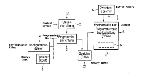
Figure 1 shows a preferred exemplifying embodiment of the inventive device,
Figure 2 shows an exemplary construction of a digital filter, and
l0
Figure 3a and Figure 3b show representations for realizing the digital filter
function
shown in Figure 2 using the inventive method.
According to the invention, to realize a desired processing function, it is
proposed to
use a programmable logic element 1 as illustrated in Figure 1, which is
reprogrammed
to execute various functoinalities that correspond to specific groups of
processing
operations. Programmable components, or respectively, logic elements, have
long
been known. One group of such logic elements that can be programmed in an
application-specific manner are what are known as field programmable gate
arrays
2 0 (FPGAs). These types of logic elements have an internal structure with
rather many
primitive cells consisting of logic gates, flip flops, and partly of simple
programmable
components (Programmable Logic Devices: PLDs). FPGAs can have several 100
terminals, or respectively, pins, and several 1000 gate equivalents and are
accordingly
suitable for realizing very complex circuits and for executing correspondingly
2 5 intensive processing functions or functionalities. As already mentioned,
FPGAs
consist of a plurality of primitive cells. Depending on the desired function
of the logic
element, these primitive cells must be wired accordingly; that is, the
connections
between the individual cells must be established. This is done by means of a
programming process, the desired configuration of the wiring typically being
stored in
CA 02320079 2000-08-04
a read-write memory (random access memory) on the FPGA chip. The logic element
executes the desired functionality depending on the configuration thus stored.
Besides the programmable logic element 1, Figure 1 also shows the programming
5 device 3 for programming the logic element 1, and the RAM memory 21 for
storing
the wiring configuration of the logic element 1 that is being instantaneously
prescribed by the programming device 3, respectively.
The programmable logic element 1 is laid out such that it applies a prescribed
l0 functionality, or respectively, processing function, such as a digital
filter function, to a
particular number of input data x. This functionality can be represented as a
combination of several groups of processing operations, such as
multiplications or
additions. Accordingly, as shown in Figure 1, the programming device 3 is so
controlled by a central control unit, which is usually formed by a computer,
that the
programming device 3 successively specifies wiring configurations for the
programmable logic element 1 which correspond to the successive groups of
processing operations, or respectively, processing procedures in the memory
21. To
this end, the device shown in Figure 1 comprises storage means in whichthe
respectively required wiring configurations are filed, depending on the
individual
2 o operations to be performed. These storage means can be constructed in the
form of
configuration files 4, so that the programming device 3 creates the conditions
for
executing the corresponding functionality blocks, or respectively, the
corresponding
processing operations, simply by loading the correspondingly stored wiring
configuration (download) and filing this wiring configuration in the memory
21. It is
2 5 also possible to use an additional memory 5; for instance, a read only
memory, in
which the respectively required wiring configurations, or respectively, the
corresponding programming data, are stored.
The function of the device represented in Figure 1 is as follows:
CA 02320079 2000-08-04
6
By means of the programmable logic element 1, the input data, that is, the
reception
data x, are to be processed in accordance with a specific processing function
(functionality). For example, the programmable logic element 1 can subject the
input
data x to a digital filtering function so that the output data y outputted by
the logic
element 1 correspond to the filtered input data x. The functionality to be
executed by
the logic element 1 is composed of a combination of several groups of
processing
operations, or respectively, subfunctionalities, which are known to the
control device
2. The central control device 2 controls the programming device 2 to read out
successive programming data by accessing the storage means 4, 5, in order to
program
l0 the logic element 1 so that the aforementioned individual groups of
processing
operations are executed in succession (or in a parallel manner). This is done
by filing
corresponding configuration data in the memory 21, so that the logic element
first
executes a first subfunctionality, such as performing multiplications, and
then a
second functionality, such as performing additions. After the execution of a
subfunctionality, intermediate results are stored by the logic element 1 in a
buffer
memory 6, so that they are available for the succeeding subfunctionalities, or
respectively, processing operations of the logic element 1. Once the control
device 2
has controlled the programming device 3 to program the logic element 1 in
accordance with the last functionality to be executed, the desired output data
y are
2 o outputted by the logic element 1.
Like the memory 21, the buffer memory 6 can be located on the chip of the
programmable logic element 1. Advantageously, the buffer memory 6 can also be
constructed in the form of a corresponding memory area within the logic
element 1,
2 5 which is indicated by broken lines in Figure l, whereby the contents of
this memory
area can be adapted with the reprogramming of the logic element, which
increases the
speed and the data throughput.
CA 02320079 2000-08-04
7
As a rule, the input data x take the form of consecutive sample values. This
means
that the above described reprogrammings of the logic element 1 are executed
for each
individual sample value, with the requirement that each reprogramming be
executed
within one sampling period of the input data x. The reprogramming speed, or
respectively, reconfiguration speed, of the programmable logic element 1
determines
its maximum sampling rate. This means that, for a high data throughput,
smaller
circuit configurations are advantageous. Accordingly, digital filters, in
particular, can
be realized very effectively by the inventive device, owing to their simple
structure.
1 o As mentioned above, the storage means 4/5 preferably contain all
programming data,
or respectively, configuration data, that are required in order to execute
specific
functionalities, or respectively, subfunctionalities of the logic element 1.
The central
control unit 2 can accordingly specify different overall functionalities or
overall
processing functions of the logic element 1 by correspondingly controlling the
programming device 3. Thus, for example, the control device 2 can reprogram
the
programmable logic element 1 by means of the programming device 3 for the
purpose
of realizing different digital filter functions with different filter
coefficients. That is,
not only is it possible to perform a reprogramming of the logic element during
the
execution of a specific processing function, but the overall functionality of
the
2 o programmable logic element 1 can also be variable. This resetting of the
overall
functionality of the logic element 1 can occur dependent on a corresponding
control
signal s, in particular, which is fed to the control device 2.
The principle of the present invention should be detailed with the aid of
Figures 2 and
3.
Figure 2 shows an example of the construction of a recursive digital filter of
second
order. The filter represented in Figure 2 comprises two shift registers 1 S,
16, three
CA 02320079 2000-08-04
8
adders 12-14, and five multipliers 7-11. The following transfer function G(z)
is
allocated to the digital filter represented in Figure 2:
G(z) _ (ao+a,z'+a2z 2)/(1-b;z'-bZZ 2)=y/x.
From the circuit diagram shown in Figure 2 it is clear that a total of five
multiplications and three additions are required for each sample value at the
input side
for executing the digital filter function during one sampling period.
Using the inventive method, the digital filter function represented in Figure
2 is
performed as illustrated in Figure 3a and Figure 3b.
When a new sample value x; is present, the programmable logic element which is
to
realize the digital filter function shown in Figure 2 is so controlled that
the
multiplications for computing the corresponding output value are performed by
the
logic element; that is, the logic element is programmed such that, for
example, the
multiplier circuit having the coefficients ao- b2 is created, as illustrated
in Figure 3.
For the forward branch, registers 17, 18 are provided, whereas only a shift
register 19
is provided for the feedback branch. The logic element 1 illustrated in Figure
1 is laid
out so that output values y; that it calculates are always stored in the
buffer memory 6,
so that, in accordance with Figure 3a, when a new sample value x; is present,
the
2 0 output value y;_~ of the previous sampling period is read out, and a shift
register for the
coefficient b, is forgone. Of course, the multiplier circuit illustrated in
Figure 3 can
also be modified in accordance with Figure 2 in that the function of the shift
register
19 is perceived by one of the two registers 17 and 18. Altogether, the shift
registers
17-19 according to Figure 3a fulfil the function of the shift registers 15 and
16 in
Figure 2. The multipliers 9-11 correspond to the multipliers in Figure 2, the
output
data of these multipliers being stored in the buffer memory 6 as the
intermediate
result.
CA 02320079 2000-08-04
9
Next, the logic element illustrated in Figure 1 is reconfigured, or
respectively,
reprogrammed, such that the logic element 1 performs the function of an adder
for
adding the data that are filed in the buffer memory 6. This functionality of
the logic
element 1 is represented in Figure 3b. As can be seen in Figure 3b, the
intermediate
results of the individual multipliers 7-11 that are stored in the memory 6 in
Figure 3a
are fed individually to an adder 20, which delivers the corresponding output
value y;
as output signal, whereby the following relation applies:
Y. ao*x.+a;*x,-1+az*x~-2+b~*Y~-t+bz*Y~-2.
As was mentioned above, the output value of the adder 20 is again stored in
the buffer
l0 memory 6, so that it is available to the multiplier circuit illustrated in
Figure 3a for
subsequent multiplication operations when a new sample value x;+, is present.
In accordance with Figure 3a and Figure 3b, the digital filter function
represented in
Figure 2 is accordingly realized in that the overall functionality of the
logic element 1
is split into two subfunctionalities; namely, performing multiplication
operations, on
one hand, and performing addition operations, on the other hand. These two
subfunctionalities are attuned to one another such that, after the last
subfunctionality
is executed, i.e. according to Figure 3b after the additions are executed, the
input data
that were processed in accordance with the original processing function, i.e.
in
2 0 accordance with the desired digital filter function, are outputted as
output data y.
Besides digital filter functions, the present invention can of course also be
used for
realizing arbitrary other functionalities, or respectively, processing
functions. One
particular instance of application is the realization of encryption or de-
encryption
2 5 functions. By means of the present invention, by appropriately programming
the
programmable logic element, completely different (encryption or de-encryption)
algorithms can be performed, which are executed in the logic element 1 either
sequentially or in a parallel manner. The control device 2 illustrated in
Figure 1 can
CA 02320079 2000-08-04
be fed a key code via the control signal s, which code specifies to the
control device 2
the order in which the individual parallel or serial conversions are to be
processed.
It is thus possible to execute encryptions or de-encryptions that correspond
to the
5 respective key code s, depending on the key code that is fed to the control
device 2, by
correspondingly reprogramming the programmable logic element 1, these
encryption
and de-encryption processes being made up of a combination of the individual
subfunctionalities of the programmable logic element 1, whose execution by the
programming device 3 in turn depends on the configuration data that are filed
in the
1 o memory 21 by the programming device 3.
The present invention is likewise suited to the realization of complex
arithmetic-logic
functions. Arithmetic-logic microprocessor units (ALUs) perform specific
processing
functions, or respectively, functionalities, by means of built-in registers
and specific
functional parts. These can be a matter of arithmetical integer operations,
logic
operations, comparison operations, or shift operations, and so on. In more
complex,
or respectively, more extensive operations, these are performed in several
steps. The
fewer clock cycles the microprocessor-controlled ALU requires for the
operation, the
faster it is. To manage this, what are known as RISC processors (Reduced
Instruction
2 0 Set Computer) were developed, which work with simpler instructions with
shorter
cyckles. [sic] By contrast, what are known as CISC processors (Complex
Instruction
Set Computer) work with a larger set of instructions and therefore require a
greater
number of clock cycles to execute complex operations.
2 5 By means of the present invention, that is, by using a programmable logic
element
that is reprogrammed during the execution of the desired processing function
to
process different groups of processing operations, parts of the ALU or even
the entire
ALU can be optimized with respect to a processing operation or several
processing
operations. As in the above described example of digital filter functions,
additions,
CA 02320079 2000-08-04
11
multiplications, and so on also occur in ALUs. Thus, to execute this
functionality, the
programmable logic element can first be programmed to function as an adder,
and the
intermediate result is stored (internally or externally). Next, the
programmable logic
element is reprogrammed to execute the function of a multiplier. For this
purpose, the
logic element accesses the intermediately stored results as well as other
potential data
or parameters and performs the desired multiplication.
In conclusion, it is noted that in order to achieve a maximum data throughput,
it is
particularly advantageous to reprogram specific circuit parts of the logic
element,
while at least one other circuit part still performs particular processing
operations, in
order to so achieve a near parallelization of the individual processing
operations
(subfunctionalities).