Note: Descriptions are shown in the official language in which they were submitted.
CA 02320740 2000-08-21
WO 99/45688 PCT/F199/00175
Redundant switching arrangement
Field of the Invention
The invention relates to providing redundancy for switching
operations regularly carried out in telecommunications systems. In particular,
the invention relates to switching elements backed up by redundant units, and
specifically to redundant switching networks. In this context, a switching
element refers to any unit or system that carries out a switching operation.
Background of the Invention
For example at telephone exchanges, a switching network is the
most important single component whose failure, may, in the worst case,
paralyse the telephone services of a larger number of subscribers. Therefore
it
is vital that the operation of the switching network can be efficiently
controlled
and that the operating personnel are immediately notified of any malfunctions
to ensure that such malfunctions are quickly located and repaired.
Traditionally, the operation of the switching network has been
protected by using two parallel switching networks that serve as mutual spare
units. Figure 1 illustrates this type of switching network arrangement with
two
parallel switching networks, SWF_A and SWF_B. Normally, the data received
at the switching network are connected to the input ports of both switching
networks (INAi and INBi, i=1,2,...n), and both switching networks operate al!
the time carrying out switching operations in the same way. As a result, the
data fed to the output ports (OUTAi and OUTBi, i=1,2,...n) are in normal
operation identical. However, only one of the switching networks is, at any
given time, selected as the active switching network whose output signals are
forwarded.
The operation of an individual switching network (SWF_A or
SWF_B) is monitored by performing internal comparative testing controlled by
the switching network control unit (CU_A, CU_B). This comparison is carried
out (see arrows) by branching off the data of selected output channels (time
slots) and that of corresponding input channels (time slots) to the control
unit
which compares the two sets of data for the duration of several frames.
Considering the total number of time slots, the actual number of channels
being compared simultaneously is normally very low to ensure that the system
does not become too complicated.
CA 02320740 2000-08-21
WO 99/45688 PC'T/FI99/00175
2
One drawback of such a redundant system is that whenever a minor
fault occurs in the equipment that induces errors in the data passing through
the switching network, this is not noticed until the internal compare test of
the
switching network happens to compare the input and output channels of that
particular switching operation. For example, in a switching network with a
maximum capacity of 2048 PCM circuits (2048 2048-kbit/s PCM signals, PCM
= Pulse Code Modulation), it takes tens of seconds to identify an error in any
single channel.
Another known method of providing redundancy is to use three
switching networks in parallel and to compare the output data of all the
switching networks. By applying the majority vote principle, the system
identifies the switching networks) that works) correctly. However, this is an
expensive solution because it requires three identical switching networks.
Summary of the Invention
The purpose of the invention is to eliminate the said drawbacks and
to provide a solution that allows the operation of a switching network or
other
switching element to be tested quickly and reliably without having to resort
to
costly hardware.
This goal is achieved by using the solution defined in the
independent patent claims.
The idea of the invention is to provide redundancy for a switching
network (or other switching element) by doubling and to test the operation of
the switching networks by comparing data in corresponding output channels,
preferably on a continuous basis. If this first comparison shows that the data
in
certain corresponding output channels are not identical, one of the switching
networks is not operating correctly. Then, an internal compare test is carried
out in at least one of the two switching networks. Because the first compare
test has already identified the output channel where the error occurred, the
internal compare test can be carried out on that particular channel and the
corresponding input channel data. Thus, the actual internal compare test is
carried out using a known method, but now the affected channels can be
selected for comparison immediately. As a result, the outcome of the compare
test is obtained immediately and the passive switching network can be quickly
activated, if the compare tests) shows) that the currently active switching
network is faulty.
CA 02320740 2000-08-21
WO 99/45688 PCT/FI99/00175
3
Another advantage offered by the solution in accordance with the
invention is that the inter-network compare test to be added to a known
switching network arrangement that uses an internal compare test can be
carried out very simply. This is due to the fact that the comparison between
the
switching networks can be performed without having to save the comparison
data because the corresponding output channels are concurrently present at
corresponding outputs of the switching networks.
In one preferred embodiment of the invention, the validity of the
connection information of both switching networks is checked after the inter-
network compare test has revealed a discrepancy relative to the output data
from the switching networks. For example, this can be effected by having the
control unit read the connection information used by the switching network and
compare this information against its own connection information. If the
connection information of both switching networks is correct, this is followed
by
an internal compare test in at least one of the switching networks. If not, an
attempt may be made to replace the incorrect connection information by
correct data, and failing that, an alarm can be given.
Brief Description of the Drawings
In the following, the invention and its preferred embodiments are
explained in greater detail with reference to Figures 2 through 8 based on the
examples given in the drawings, where
Figure 1 illustrates a known redundant switching network;
Figure 2a illustrates a redundant switching network in accordance with the
invention;
Figure 2b illustrates comparison of corresponding channels;
Figure 3 is a flowchart illustrating the method in accordance with the
invention;
Figure 4 illustrates the functional blocks of a known telephone exchange;
Figure 5 illustrates an implementation of the switching network at the
telephone exchange shown in Figure 4;
Figure 6 shows the telephone exchange of Figure 4 with a backed-up
switching network;
Figure 7 illustrates the performance of the compare test between switching
networks in the switching network shown in Figure 5; and
CA 02320740 2000-08-21
WO 99/45688 PCT/F199/00175
4
Figure 8 illustrates the performance of the internal compare test in the
switching network shown in Figure 5.
Detailed description of the invention
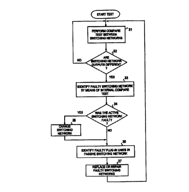
In the following, a solution according to the invention is first
described on a general level with reference to Figures 2a, 2b and 3. Figure 2a
illustrates the switching arrangement shown in Figure 1 with redundant
switching networks, while Figure 3 is a flowchart illustrating the steps of
the
method according to the invention. As suggested by the invention, the
operation of the switching networks is monitored by comparing the data in two
corresponding output channels (comparators C1...Cn, Figure 2a, and step 31,
Figure 3). Figure 2b illustrates the comparison of two corresponding output
channels assuming that transmission is carried out in successive time slots
the
number of which per each transmission frame FR is pre-defined. The frames
appear in the corresponding output ports in the same phase, and so the
corresponding time slots (channels) occur simultaneously and comparison can
be carried out without having to save the data in between.
Preferably, comparison between the switching networks is carried
out on a continuous basis and if no discrepancy is detected, a new compare
test between the switching networks is performed. If a discrepancy is detected
between one or more output channel pairs, an internal compare test (Figure 3,
step 33) is carried out in one, but preferably both, switching networks in
order
to identify the incorrectly operating switching network.
In an internal compare test, the data from the faulty output channel
and the data from the input channel corresponding (according to the switching
operation used) to that output channel are branched off to the control unit
from
the input and output ports involved. The switching network where the input and
output data differ from each other is faulty.
Once the internal compare test has identified the faulty switching
network, the active switching network is deactivated {step 35) and the passive
switching network activated, if the fault exists in the active switching
network.
If, on the other hand, it is determined that the fault lies in the passive
switching
network, the active switching network is allowed to remain active.
Interchanging the switching networks can be effected by having the control
unit
send a signal to the switching networks and connected units to indicate which
CA 02320740 2000-08-21
WO 99/45688 PCT/FI99/00175
5
switching network is currently active. Thus, the units involved will know the
switching network whose signals should be allowed to pass through.
After these steps have been taken, the fault will exist in the passive
switching network, making it possible to identify the faulty plug-in units
(one or
several) (step 36). Following repairs to the defective components (step 37),
compare testing between the switching networks can be resumed.
When a discrepancy is detected in one or more output channel
pairs, it is possible first to check the switchings before any internal
compare
tests) is/are initiated. If the connection information are found to be
correct, an
internal compare test will be started in at least one of the switching
networks. If
the connection information are found to be incorrect, the control unit will
make
an attempt to replace the incorrect connection information with correct data.
Failing that, the operating personnel will be alerted. !f the connection
information can be successfully fixed, compare testing between the switching
networks is resumed.
A more detailed description of one embodiment of the invention is
provided below using the switching arrangements common in the conventional
TDM network as examples.
In conventional TDM (Time Division Multiplexing) networks, data are
transmitted as a bit or symbol stream in time slots, each containing a certain
number of bits, typically eight. In conventional PCM systems, these bits in
any
single time slot are all reserved to one and the same channel. For example, in
the European 2048 kbit/s basic multiplexing system (where the frame length is
32 time slots, i.e. 256 bits), it is possible to transmit a total of 30 voice
channels, each with a capacity of 64 kbit/s. (In the corresponding U.S.
system,
the number of channels is 24 and the transmission rate 1544 kbit/s.) A
description of a solution based on the invention is provided below, adapted to
a telephone exchange in a TDM network.
Figure 4 illustrates the functional blocks of a telephone exchange
system as used, for example, in the applicant's DX 210 telephone exchange.
The core of the exchange consists of the switching network SWF whose task
is to interconnect input and output channels. Switching takes place under the
control of the call control unit CAC. The call control unit CAC is in charge
of all
decision making relating to call control. The larger DX 220 exchange, also
manufactured by the applicant, makes use of decentralised call control by
distributing the functions required for call control between several computer
CA 02320740 2000-08-21
WO 99/45688 PCT/F199/00175
6
units. Data between these units are transmitted via the message bus MB.
Operation and maintenance of the exchange is effected by means of the
operation and maintenance unit OMU. Peripheral equipment such as display
terminals and printers are connected to the operation and maintenance unit.
Subscribers are connected to the exchange by means of subscriber
modules SUB. The interface can be a standard analog interface or a digital
ISDN interface. The subscriber modules carry out the AID and D/A
conversions required for analog interfaces and handle signalling operations
between the subscriber terminal (telephone) and the exchange.
The exchange is connected to other exchanges or remote
subscriber stages by means of trunk circuit interfaces ET. The external
interface of the exchange conforms to the CCITT (currently ITU-T) 6.700
series recommendations.
In a system as described above, the switching network SWF can, for
example, be designed as shown in Figure 5. The design is identical to that
used in the applicant's DX 210 and DX 220 exchanges. The structural
components of the switching network are the converter units SPSi (i=1...32)
and switching blocks SWEi~ (i=1...8, j=1...8). In practice, the control unit
of the
switching network consists of four plug-in units, but, for the sake of
simplicity,
the figure only shows one shared control unit CU (which is part of the call
control unit CAC shown in Figure 4).
Data are transmitted between the subscriber modules SUB and the
converter units via the 4 Mbit/s serial buses SB, numbering 32 per converter
unit. Each 4 Mbit/s serial bus contains the contents of two 2 Mbit/s PCM
circuits multiplexed on a time division basis (64 kbit/s channels). The data
used for testing in accordance with the invention are branched off at this 4
Mbit/s interface, as will be explained below. As a result, the capacity of the
switching network used as the example is 2x32x32 = 2048 PCM circuits (2048
2048 kbit/s PCM signals).
The 4 Mbit/s serial buses from the subscriber modules are converted
by serial-to-parallel converters into a single parallel bus with a capacity of
16.384 Mbytes/s. The parallel bus IBi (i=1...32) from each converter unit
connects to eight switching blocks shown in the figure on the same horizontal
line. The parallel buses from converter units SPS1...SPS4 connect to
switching blocks SWE;, (i=1...8), those from converter units SPSS...SPS8 to
the switching blocks SW E;2 (i=1...8), and so on, and the parallel buses from
CA 02320740 2000-08-21
WO 99/45688 PC'f/F199/00175
7
converter units SPS29...SPS32 to switching blocks SWE;$ (i=1...8).
Consequently, there are a total of four parallel buses from four separate
converter units to each switching block (one from each converter unit).
Conversely, there are a total of four (16.384 Mbit/s) parallel buses
from each switching block to four separate converter units (one to each unit).
The switching blocks shown in the figure on the same vertical line drive the
same output bus that connects to one converter unit. In other words, switching
blocks SWE1~ Q=1...8) drive bus OB1 that connects to converter unit SPS1,
bus OB2 that connects to converter unit SPS2, bus OB3 that connects to
converter unit SPS3, and bus OB4 that connects to converter unitSPS4, while
switching blocks SWE2~ (j=1...8) drive bus OB5 that connects to converter unit
SPSS, bus OB6 that connects to converter unit SPS6, bus OB7 that connects
to converter unit SPS7, and bus OB8 that connects to converter unit SPSB,
and so on, and switching blocks SWE~ (j=1...8) drive bus OB29 that connects
to converter unit SPS29, bus OB30 that connects to converter unit SPS30, bus
OB31 that connects to converter unit SPS31, and bus OB32 that connects to
converter unit SPS32.
At each individual converter unit, the 4 Mbit/s serial buses
(numbering 32) are formed from the parallel bus coming from the switching
blocks by pertorming a parallel-to-serial conversion on the incoming data.
Thus, each converter unit transmits to eight different switching
blocks (shown on the same horizontal line in the figure) and receives from
eight switching blocks (shown on the same vertical fine in the figure), making
it
possible to switch any incoming time slot to any outgoing time slot.
Control unit CU connects directly to each converter unit and each
switching block via control bus CB.
The switching blocks SWE;~ receive and transmit data via the said
parallel buses. In the switching block, the incoming parallel data are written
cyclically, byte by byte, to the switching memory. In the outgoing direction
of
transmission, data transmission is controlled by the control memory in the
switching block, to which the control unit has written, via the control bus,
the
read address for the switchings to be made. The control memory is read
cyclically in time with the outgoing time slots. The read address in the
control
memory indicates the address in the switching memory from which the data for
the time slot involved should be read. Thus, the actual cross-connection is
effected using a known method.
CA 02320740 2000-08-21
WO 99/45688 PCT/F199/00175
8
When the method in accordance with the invention is used, the
switching network, as described above, is backed-up by providing redundancy
as shown in Figure 6, where there are two parallel switching networks (SWF_A
and SWF_B) as shown in Figure 5, one of which is selected for active
operation. The units {SUB, ET) connecting to the switching network select the
data transmitted by the active network. In this example, both switching
networks have their own control units.
Figure 7 illustrates one way of applying inter-network comparison to
the type of switching network described in the foregoing. As indicated above,
this comparison can, for example, be carried out in the converter units. All
the
functions in the various converter units are identical, so~ that the following
explanation applies to both switching networks. In the figure, the elements
belonging to the first switching network {SWF_A) are denoted by the letter A
and the elements belonging to the second switching network (SWF_B) by the
letter B.
The PCM signals from an individual converter unit towards the
subscriber module, numbering 32 in this example, are denoted by TO...T31.
For comparison, these signals are branched off to a separate multiplexes M1
to whose output one incoming signal at a time is connected for the duration of
one frame (125 ~.s). The multiplexes output is connected both to the first
input
of the own comparison unit COMP and to the second input of the comparison
unit in a converter unit belonging to the other switching network. In this
example, the converter units SPS_A and SPS_B are interconnected by two 4
Mbit/s interfaces. Multiplexes M1 is controlled by a branching logic unit BLU,
which is used to select the signal to be compared at any given time. The
branching logic units are synchronised to ensure that they always select the
same signal.
Comparison unit COMP compares corresponding channels during
one frame, after which it analyses the corresponding channels of the following
(4 Mbit/s) signal. Thus, the comparison unit carries out comparison for 64
channel pairs during a single frame. As a result, all the channels can be
checked during 32 frames. This also means that an error in any signal is
detected within a period of time equivalent to the duration of 32 frames, if
not
earlier (which is a short time compared with the conventional solution). The
serial data coming in from multiplexes M1 are stored, after which comparison
is
carried out byte by byte (channel by channel) using a known method. The
CA 02320740 2000-08-21
WO 99/45688 PCT/FI99/00175
9
comparison unit indicates whether the bytes in the corresponding channels
differ from one another. This item of data is written to the buffer memory BM
together with the data indicating the channel involved. The latter data are
obtained from the branching logic unit. Thus, the buffer memory receives
information, channel by channel, as to whether the contents of each channel
are identical in both switching networks.
Control unit CU reads the contents of the buffer memory via control
bus CB, and if it detects an error (discrepancy) in any outgoing channel pair,
it
starts the internal compare test for the switching networks. Because the
control
unit is aware of the switchings to be made, it is capable of targeting the
compare test to the output channel suspected of failure and the corresponding
input channel. The control unit reads the contents of the buffer memories of
all
the converter units during one frame.
In the examples detailed above, 1 signal out of 32 is selected at any
one time for comparison. This helps to achieve a compromise between the
speed of detection of a fault and the complexity of the equipment. If faults
are
to be detected more quickly, several signals must be compared
simultaneously. This also calls for increased data transmission capacity
between the converter unit and the control unit.
Because both switching networks basically include identical
hardware, the compare test between the switching networks can be carried out
in both switching networks. However, since the output channels of only the
active switching networks are used, it is natural that use is only made of the
compare test result of the active switching network. Thus, the control unit of
the active switching network gives the control unit of the passive switching
network the command to start the internal compare test within that switching
network. However, a compare test between the switching networks can only
be performed in one of the switching networks (the same applies to the
internal compare test within the switching network).
The principle of the internal compare test is illustrated in Figure 8 for
one converter unit SPSi. The test works in the same way for other converter
units also.
Comparison between the input and output channels is carried out by
switching network control unit CU, not by the converter unit, as in the
compare
test between the switching networks. To start comparison, the control unit
gives a branching command via control bus CB to the converter unit SPSi
CA 02320740 2000-08-21
WO 99/45688 PCT/F199/00175
10
corresponding to the input and output channel (i=1...32 and may have 1 or 2
values). In response to the branching command, the converter unit branching
logic BLU branches off the time slots involved to the control unit via the
control
bus. In the control unit, comparison logic CL compares the contents of the
input and output channels corresponding to the switching involved. The
comparison logic reports the results of the test to the control unit
microcomputer MC which makes the decision on the further action required.
Testing of the faulty passive switching network can, for example, be
carried out using the through-connection test. This test differs from the
internal
compare test of the switching networks in that the converter unit transmits a
test byte assigned by the control unit to the time slots coming into the
switching
network. The control unit starts the through-connection test by writing the
test
byte to the converter unit test register {not shown) via control bus CB. The
outgoing time slots of the connection to be tested are branched off from the
converter unit via the control bus to the control unit whose comparison logic
compares the contents of the outgoing time slot to the test byte transmitted
to
the converter unit corresponding to the incoming time slot. In other words,
branching and comparison of time slots is carried out using the same principle
as in internal compare testing, except that incoming time slots are not
branched off to the control unit because the contents of the incoming time
slots (test bytes) are already known to the control unit.
Figures 7 and 8 show, on a general level, only those components
that are essential to the performance of the tests. For example, in addition
to
branching logic, Figure 8 only shows, for the converter unit, the interfaces
that
carry out the parallel-to-serfal conversion (PISO) on the side of the
switching
blocks, and the serial-to-parallel conversion (SIPO) in the opposite direction
of
transmission. Moreover, the same branching logic (BLU) is shown performing
branching for both tests.
Both in the compare test between switching networks and in the
switching network internal compare test, it is preferable to carry out the
comparison by comparing the bytes or bit sequences involved directly.
However, it is also possible to perform this comparison indirectly by using
some function to compute a provisional result, such as a check sum, from the
bytes or bit sequences to be compared and then comparing these provisional
results. The same applies to the through-connection test.
CA 02320740 2000-08-21
WO 99/45688 PCT/F199/00175
11
Although the invention has in the foregoing been explained with
reference to the examples shown in the attached drawings, it is clear that the
invention is not limited to these embodiments but can be varied within the
scope of the basic idea of the invention as presented in the enclosed patent
claims. For example, even though the principle based on the invention has
been described above in connection with a switching network used in a TDM
network, the same principle can be used to provide redundancy for a switching
network in a packet-switched network, such as ATM network. In such a case,
the packets or cells of one virtual connection are compared at corresponding
output ports, and if any discrepancy is detected, the packets (or cells) are
then
compared at the output and input ports of both switching networks (the packet
present at the input port is compared with the same packet at the output
port).
Also, the compare test between switching networks or the internal compare
test need not necessarily be carried out in both switching networks, but both
tests can be carried out in only one of the two switching networks. If the
(internal) test performed in the switching network (or in its control unit)
gives
the correct result, it is clear that the fault lies in the other switching
network
(and vice versa). Comparisons can also be carried out outside the actual
switching network, as explained above for the internal compare test. Nor is
the
solution according to the invention tied to providing the entire switching
network, but the same principle can be applied to any element performing
switching operations, such as a switching element in the switching network.
Therefore, the term 'switching element' used in the enclosed patent claims
must be understood as covering a range of options. Switching networks (or
elements) may also share a single control unit backed-up by a redundant unit.