Note: Descriptions are shown in the official language in which they were submitted.
CA 02320785 2000-08-18
- 1 -
SPECIFICATION
DEMODULATING APPARATUS OF RECEIVER
Technical Field
s The present invention relates to a demodulating apparatus of a
receiver, and more specifically to a demodulating apparatus of a
receiver for demodulating a PSK modulated signal obtained by
time-multiplexing a digital signal modulated in a 2-phase, 4-phase,
and 8-phase PSK modulation system in a hierarchical transmission
to system, etc. by using a carrier regenerated by carrier regeneration
means, and outputting an I-Q symbol stream data.
Background Art
A digital satellite TV broadcast in a plurality of modulation
i5 systems in which different necessary C/Ns are required, for example,
in a hierarchical transmission system in which an 8 PSK modulated
wave, a QPSK modulated wave, and a BPSK modulated wave are
time-multiplexed and repeatedly transmitted for each frame has been
developed for practical use.
2 o Fig. 8 shows an example of the configuration of one
transmission frame in the hierarchical transmission system. One
frame includes a frame synchronous signal pattern (predetermined
20 symbols are actually used as a frame synchronous signal in 32
symbols) formed by 32 BPSK-modulated symbols, a TMCC
25 (transmission and multiplexing configuration control) pattern for
CA 02320785 2000-08-18
- 2 -
transmission multiplexing configuration identification formed by 128
BPSK-modulated symbols, a superframe identification pattern farmed
by 32 symbols (predetermined 20 symbols are actually used as a
superframe identification signal in 32 symbols), a main signal having
s 203 8 PSK (trellis codec 8 PSK) modulated symbols, a 4-symbol burst
symbol signal (BS) obtained by BPSK-modulating a pseudo random
noise (PN) signal, a main signal having a 203 8 PSK (trellis codec 8
PSK) modulated symbols, a 4-symbol burst symbol signal (BS)
obtained by BPSK-modulating a pseudo random noise (PN) signal, ...,
io a main signal having 203 QPSK-modulated symbols, a 4-symbol
burst symbol signal (BS) obtained by BPSK-modulating a pseudo
random noise (PN) signal, a main signal having 203 QPSK-modulated
symbols, and a burst symbol signal (BS) having 4 BPSK-modulated
symbols in this order.
1 s Here, the mapping for each modulation system on the
transmission side will be described below by referring to Figs. 9A-9C.
Fig. 9A shows a signal point arrangement at the I-Q phase (an I-Q
vector or an I-Q signal space diagram) when the 8 PSK modulation
system is used. In the 8 PSK modulation system, a 3-bit digital
2 o signal (abc) can be transmitted as 1 symbol, and there can be 8
combinations of bits forming 1 symbol, that is, (0 0 0), (0 0 1), (0 1 0),
(0 1 1), (1 0 0), (1 0 1), (1 1 0), and (1 1 1). These 3-bit digital signals
are converted into the signal point arrangements 0 through 7 in the
I-Q phase on the on the transmission side as shown in Fig. 9A. The
2s conversion is referred to as 8 PSK mapping.
CA 02320785 2000-08-18
- 3 -
In an example shown in Fig. 9A, the bit string (0 0 0) is
converted into the signal point arrangement '0', the bit string (0 0 1)
is converted into the signal point arrangement ' 1', the bit string (0 1
1) is converted into the signal point arrangement '2', the bit string (0
s 1 0) is converted into the signal point arrangement '3'; the bit string
( 1 0 0) is converted into the signal point arrangement '4', the bit
string (1 0 1) is converted into the signal point arrangement 'S', the
bit string (1 1 1) is converted into the signal point arrangement '6',
and the bit string ( 1 1 0) is converted into the signal point
i o arrangement ' 7' .
Fig. 9B shows the signal point arrangement at the I-Q phase
when a QPSK modulation system is used. In the QPSK modulation
system, a 2-bit digital signal (de) can be transmitted as 1 symbol, and
there can be 4 combinations of bits as a symbol. They are (0 0), (O1),
i5 (10), and (11). In the example shown in Fig. 9B, for example, the bit
string (0 0) can be converted into the signal point arrangement ' 1', the
bit string (0 1) can be converted into the signal point arrangement '3',
the bit string (1 1) can be converted into the signal point arrangement
'S', and the bit string ( 1 0) can be converted into the signal point
2o arrangement '7'.
Fig. 9C shows the signal point arrangement when a BPSK
modulation system is used. In the BPSK modulation system, a 1-bit
digital signal (f~ can be transmitted as 1 symbol. In the digital signal
(f], for example, the bit (0) is converted into the signal point
2 s arrangement '0' , and the bit ( 1 ) is converted into the signal point
CA 02320785 2000-08-18
- 4 -
arrangement '4'. The relationship between the signal point
arrangement and the arrangement number in each modulation
system is defined such that the signal point arrangement is
equivalent to the arrangement number based on the 8 BPSK.
s The I axis and the Q axis of the QPSK and the BPSK in the
hierarchical transmission system match the I axis and the Q axis of
the 8 PSK.
Eight frames shown in Fig. 8 form one superframe. In the area
of 20 predetermined symbols of a frame synchronous signal pattern
1 o in each frame, a well-known 20-bit digital signal pattern (referred to
as W ~) is BPSK-mapped. In the area of 20 predetermined symbols of
a superframe identification signal pattern as a leading frame in a
superframe, a well-known 20-bit digital signal pattern (referred to as
W2) different from W 1 is BPSK-mapped. In the area of 20
i5 predetermined symbols of a superframe identification signal pattern
in each frame other than the leading frame in a superframe, a
well-known 20-bit digital signal pattern (referred to as Wa, and
obtained by inverting each bit of W2) is BPSK-mapped.
In the receiver for receiving a digital modulated wave (PSK
a o modulated wave) in the hierarchical transmission system, the
intermediate frequency signal of a signal received by a reception
circuit is demodulated through orthogonal detection by a
demodulating circuit, thereby obtaining two sequences of I-Q base
band signals (hereinafter, the I-Q base band signal can also be
2 s referred to as I-Q symbol stream data) indicating the momentary
CA 02320785 2000-08-18
- 5 -
value for each symbol of the I axis and the Q axis orthogonal to each
other. However, when there is a shift in phase between the carrier
before the modulation of an input of the demodulating circuit and the
reference carrier regenerated in the demodulating circuit, the received
s signal point of the modulated I-Q base band signal is phase-rotated
toward the transmission side. Therefore, the digital signal
transmitted on the transmission side cannot correctly recover if the
data is input as it is to the decoder and PSK-mapped.
Each of the burst symbol signals (BS) shown in Fig. 8 is
to obtained by resetting the PN code generator having a predetermined
configuration at the starting position of the initial burst symbol signal
(BS) in a frame on the transmission side, shifting the output
according to the symbol clock at each period in the transmission
frame configuration, and performing a BPSK mapping process.
is The demodulating circuit uses a burst symbol signal (BS) as a
pilot signal for amendment of the phase of the reference carrier, and
allows the phase of the carrier in the state before the modulation of
the received signal to match the phase of the reference carrier,
thereby setting the absolute phase such that the signal point of the
2 o I-Q base band signal output from the demodulating circuit as
matching the signal point on the transmission side.
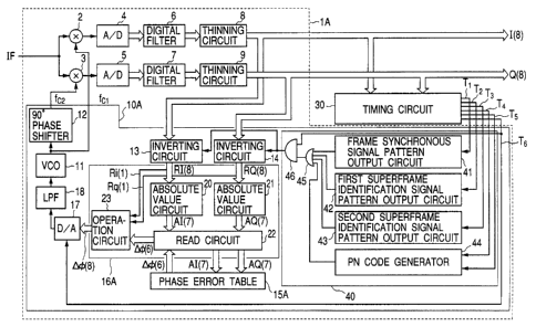
Fig. 10 shows the configuration of the demodulating circuit of
the receiver for receiving the PSK modulated wave in the conventional
hierarchical transmission system. A demodulating circuit 1 shown
2 s in Fig. 10 obtains an I-Q base band signal by orthogonally detecting
CA 02320785 2000-08-18
- 6 -
the intermediate frequency signal of a received signal. 10 denotes a
carrier regeneration circuit for regenerating two reference carriers f~ 1
(= cos wt~, and f°2 (= sin wt) whose frequencies and phases are
synchronized with those of the carrier in the state before the
s modulation of the input of the demodulating circuit 1, and whose
phases are 90° shifted to each other to be orthogonal to each other.
2 and 3 denote multipliers for multiplying the intermediate frequency
signal IF by the reference carriers f~l and f~2. 4 and S denote A/D
converters for A/ D converting the output of the multipliers 2 and 3 at
to a sampling rate of double the symbol rate. 6 and 7 denote digital
filters for limiting the band in a digital signal process performed on
the output of the A/D converters 4 and 5. 8 and 9 denote thinning
circuits for thinning the output of the digital filters 6 and 7 at the
sampling rate of 1/2, and outputting two sequences of I-Q base band
is signals (I-Q symbol stream data) indicating the momentary value of
each symbol of the I axis and the Q axis. The thinning circuits 8
and 9 transmit the I-Q base band signals I (8) and Q (8) (the
numerals in the parentheses denote the numbers of quantization bits,
which will be hereinafter referred to simply as I-Q for short) having 8
20 (complement of 2) quantization bits.
If the phase of a carrier in the state before modulation at the
input of the demodulating circuit 1 matches the phase of the
reference carriers f~~ and f~2 regenerated by the carrier regeneration
circuit 10, then the phase of the received signal point in the I-Q
2s phase by the I-Q base band signals I (8) and Q (8) on the reception
CA 02320785 2000-08-18
side when the digital signal corresponding to the signal point
arrangement '0' through '7' in the I-Q phase on the transmission side
is received matches the phase on the transmission side. Therefore,
the digital signal received from the signal point arrangement of the
s received signal point can be correctly identified by directly using the
correspondence (refer to Fig. 9A-9C) between the signal point
arrangement on the transmission side and the digital signal.
However, since the reference carriers f~~ and f~2 can be actually
in various phase states for the carrier in the state before the
to modulation of the input of the demodulating circuit 1, the received
signal point on the reception side is the phase position set by turning
from the position on the transmission side by a predetermined angle
0. When the phase of the carrier in the state before the modulation
of the input of the demodulating circuit 1 is changed, the angle A is
i5 also changed. If the phase of the received signal point rotates at
random from the phase on the transmission side, then the received
digital signal cannot be identified. For example, at the time of 6 =
~/8, the digital signal (0 0 0) as the signal point arrangement '0' in
the 8 PSK modulation system on the transmission side has the
2o received signal point between the signal point arrangements '0' and
' 1' on the reception side. Therefore, if it is assumed that the digital
signal (0 0 0) is received at the signal point arrangement '0', it is
correctly received. However, if it is assumed that the signal is
received at the signal point arrangement ' 1', it is mistakenly
2s recognized that a digital signal (0 0 1) has been received. Then, the
CA 02320785 2000-08-18
_ g _
carrier regeneration circuit 10 amends the phase of the reference
carriers f~ 1 and f~2 such that the received signal point can match the
point on the transmission side to correctly identify the digital signal.
Specifically, the reference carrier f~~ is generated by oscillating a
s VCO (voltage control oscillator) 11 of the carrier regeneration circuit
10, and the reference carrier f~2 is generated by 90° delaying the
phase of the oscillation signal of the VCO 11 by a 90° phase shifter
12. Then, the phase of the reference carriers fm and f~2 can be
variable by varying the control voltage of the VCO 11.
io In the carrier regeneration circuit 10, 13 and 14 are inverting
circuits for selectively inverting the code of an I-Q base band signal
output from the demodulating circuit 1 according to an output value
of a well-known pattern regeneration circuit described later. 15
denotes a phase error table containing a phase error from an
15 absolute phase for a received signal point in the state of the output of
the inverting circuits 13 and 14, and includes ROM. In this example,
as described later, the absolute phase is fixed to 0 (= 2n). Fig. 11
shows the relationship between the phase angle ~ made by the
received signal point of the I-Q phase in the state of the output of the
2 o inverting circuits 13 and 14 and the positive direction of the I axis
and the phase error data 0~. The phase error data ~~ represents 8
quantization bits (complement of 2).
16 denotes a phase error detecting processing circuit for
reading the phase error data 0~ (8) corresponding to the output of the
as inverting circuits 13 and 14 from the phase error table 15, and
CA 02320785 2000-08-18
g _
outputting it to a D/A converter 17. After the phase error data 0~ (8)
is converted into a phase error voltage by the D/A converter 17, the
lower band element is extracted by an LPF 18, and is applied as a
control voltage to the VCO 11. If the phase error data ~~ (8) is 0,
s then an output of the LPF 18 is not changed, and the phases of the
reference carriers f~~ and f~2 are not changed. However, if the phase
error data e~ (8) is positive (+), an output of the LPF 18 becomes large,
the phases of the reference carriers f~l and f~2 are delayed. On the
other hand, if the phase error data 0~ (8) is negative (-), an output of
to the LPF 18 becomes small, and the phases of the reference carriers f~l
and f~2 are forwarded.
A timing circuit 30 is provided on the output side of the
demodulating circuit 1, detects the starting timing in each symbol
period corresponding to the frame synchronous signal pattern W ~,
is and the superframe identification signal patterns W2 and Ws
regardless of the existence/non-existence of the phase rotation as
compared with the transmission side of the I-Q base band signal, and
outputs timing signals T1 through Ta. Furthermore, it detects a
starting timing of the first burst symbol signal (BS) in a frame, and
20 outputs a timing signal T4. In addition, it detects the period of the
burst symbol signal (BS), and detects a period signal Ts indicating 'H'
for the period of the burst symbol signal, and 'L' for other periods.
Furthermore, it detects a symbol period corresponding to a
superframe identification signal pattern W ~, and a symbol period
2s corresponding to superframe identification signal patterns W2 and Wa,
CA 02320785 2000-08-18
- 10 -
and outputs a period signal T~ indicating 'H' for the above described
periods and the period of the burst symbol signal (BS), and indicating
'L' for other periods (refer to Figs. 12 and 13j.
40 denotes a pattern regeneration circuit, 41 denotes a frame
s synchronous signal pattern output circuit for outputting a 20-bit
frame synchronous signal pattern W 1 in the period of 20 symbols
from the input timing of T1, 42 denotes a first superframe
identification signal pattern output circuit for outputting a 20-bit
superframe identification signal pattern W2 in the period of 20
to symbols from the input timing of T2, 43 denotes a second superframe
identification signal pattern output circuit for outputting a 20-bit
superframe identification signal pattern Ws in the period of 20
symbols from the input timing of Ta, 44 denotes a PN code generator,
has the same configuration as the PN code generator for generating a
is PN code string for a burst symbol signal (BS) on the transmission
side, changes its output according to a symbol clock while the period
signal Ts indicates 'H' after it is reset at the starting timing of the first
burst symbol signal (BS) in the frame according to T4, and outputs
the same pattern as the PN code pattern before the BPSK mapping of
ao each burst symbol signal (BS) in the output of the demodulating
circuit 1 at the same timing as the burst symbol signal (BS).
45 denotes an OR circuit for outputting a logical sum of the
outputs of the frame synchronous signal pattern output circuit 41,
the first superframe identification signal pattern output circuit 42,
2s the second superframe identification signal pattern output circuit 43,
CA 02320785 2000-08-18
- 11 -
and the PN code generator 44. 46 is an AND circuit for obtaining a
logical product of the OR circuit 45 and the period signal T~.
The above described pattern regeneration circuit 40 regenerates
a corresponding bit string pattern for the symbol corresponding to
s the 20-bit frame synchronous signal pattern W ~ appearing in the I-Q
symbol stream output from the demodulating circuit 1, the symbol
corresponding to the 20-bit superframe identification signal patterns
W2 and Ws, and the burst symbol signal (BS). The W1, Wz, and Ws,
and the PN code before the BPSK mapping of the burst symbol signal
to (BS) are well-known bit string patterns on the transmission side, and
are BPSK-mapped. As shown in Fig. 9C, the bit 0 is mapped at the
signal point arrangement '0' (absolute phase 0) on the transmission
side, and the bit 1 is mapped at the signal point arrangement ' 1'
(absolute phase ~) on the transmission side.
is The above described inverting circuits 13 and 14 respectively
output the I-Q base band signals I (8) and Q (8) output from the
demodulating circuit 1 as they are when the output of the pattern
regeneration circuit 40 is a bit '0'. At this time, the original absolute
phase in the state on the transmission side of the received signal
2o point indicated by the output RI (8) = I (8), RQ (8) = Q (8) is 0. On
the other hand, the inverting circuits 13 and 14 inverts and outputs
the code of the I-Q base band signal output from the demodulating
circuit 1 when the output of the pattern regeneration circuit 40 is a
bit ' 1'. Inverting a code is forwarding the phase of a received signal
25 point by n, and this indicates that the original absolute phase on the
CA 02320785 2000-08-18
- 12 -
transmission side of the received signal point indicated by the
outputs RI (8) _ -I (8), and RQ (8) _ -Q (8) of the inverting circuits 13
and 14 can also be assumed to be 0 (= 2~c).
The phase of the received signal point after demodulating the
s transmission signal BPSK-mapped at the bit '0' on the transmission
side can be amended into 0 by reading the phase error data 0~ (8)
corresponding to the output of the inverting circuits 13 and 14 from
the phase error table 15 when the output of the pattern regeneration
circuit 40 is '0', and amending the phases of the reference carriers f~l
1 o and f~2 such that the phase error data ~~ (8) can be zero. Similarly,
the phase of the received signal point after demodulating the
transmission signal BPSK-mapped at the bit '0' on the transmission
side can be amended into ~c by reading the phase error data ~~ (8)
corresponding to the output of the inverting circuits 13 and 14 from
1 s the phase error table 1 S when the output of the pattern regeneration
circuit 40 is ' 1', and amending the phases of the reference carriers f~l
and f~2 such that the phase error data 0~ (8) can be zero. Therefore,
the demodulating circuit 1 can output an absolute-phase I-Q base
band signal, and the decoder at a later stage can perform a PSK
2 o demapping process without fail.
The D/A converter 17 D/A converts and outputs the phase
error data 0~ (8) in the period only when the period signal T6 at the H
level is input from the timing circuit 30. While the T6 indicates the L
level, the D/A converter 17 holds the last output value obtained when
25 the T6 indicated the H level immediately before.
CA 02320785 2000-08-18
- 13 -
However, in the conventional receiver described above, it is
necessary to define a phase error table for the entire range from the
first quadrant to the fourth quadrant in the I-Q phase indicated by
the outputs of the inverting circuits 13 and 14, thereby causing the
s problem of large memory requirements.
The present invention aims at providing a demodulating
apparatus of a receiver requiring only a small circuit.
Disclosure of the Invention
to The demodulating apparatus according to claim 1 for use in a
receiver having a demodulating unit for demodulating a PSK
modulated signal obtained by time-multiplexing digital signals
modulated in various PSK modulation systems by using a carrier
regenerated by a carrier regeneration unit, and outputting I-Q symbol
is stream data in a symbol unit includes: regeneration means for
regenerating a digital signal of a predetermined pattern for a 2-phase
modulated portion in the output of the demodulating means on the
transmission side; inverting means for selectively code-inverting the
I-Q symbol stream data output from the demodulating unit based on
2 o the value of a predetermined pattern regenerated by the regeneration
means; a phase error table showing the phase error from the absolute
phase for the received signal point in a predetermined quadrant; and
phase error detecting means for converting a received signal point in
the I-Q phase indicated by an output of the inverting unit into the
Zs one in a predetermined quadrant by performing a process depending
CA 02320785 2000-08-18
- 14 -
on the current quadrant, reading the phase error data corresponding
to the converted received signal point from the phase error table, and
adjusting .the read phase error data depending on the conversion.
With the configuration, the carrier regeneration means amends the
s phase of the regenerated carrier according to the phase error data
adjusted by the phase error detecting means.
The PSK modulated signal obtained by time-multiplexing the
digital signal modulated in the 2-phase, 4-phase, and 8-phase PSK
modulation system is demodulated using a carrier regenerated by the
to carrier regeneration means, and output as the I-Q symbol stream
data in a symbol unit by the demodulating unit. The regeneration
unit regenerates a well-known pattern for the portion obtained by
2-phase modulating the digital signal of the well-known pattern on
the transmission side in the output of the demodulating unit, and the
is inverting unit selectively code-inverts the I-Q symbol stream data
output from the demodulating means based on the value of the
well-known pattern. The phase error table contains a phase error
from the absolute phase for the received signal point in a
predetermined quadrant in the I-Q phases indicated by the output of
2o the inverting means. The phase error detecting means performs a
process by combining any of the no-conversion process, the
symmetric conversion about the I axis, the symmetric conversion
about the Q axis, the symmetric conversion about the I=Q axis, and
the symmetric conversion about the I=-Q axis, reads from the phase
2s error table the phase error data corresponding to the received signal
CA 02320785 2000-08-18
- 15 -
point converted in the predetermined quadrant defined in the phase
error table, adjusts the read phase error data based on the
combination of the conversion, and obtains the phase error data from
the absolute phase for the received signal point in the I-Q phase
s indicated by an output of the inverting means. The carrier
regeneration means amends the phase of the regenerated carrier
based on the phase error data detected by the phase error detecting
means.
According to the present invention, the phase error table can
to contain a phase error from the absolute phase for the received signal
point in a predetermined quadrant in the first through the fourth
quadrants in the I-Q phase, thereby considerably simplifying the
circuit configuration.
15 Brief Description of the Drawings
Fig. 1 is a block diagram of the configuration of a principal part
of a PSK modulated wave receiver according to an embodiment of the
present invention;
Fig. 2 shows the defined area of a phase error table shown in
2 o Fig. 1;
Fig. 3 shows the relationship between a phase angle of a
received signal point and a phase error data in the phase error table
shown in Fig. 1;
Fig. 4 shows the operation of an absolute value circuit shown in
2 s Fig. 1;
CA 02320785 2000-08-18
- 16 -
Fig. 5 shows the operation of the absolute value circuit shown
in Fig. 1;
Fig..6 shows the operation of the absolute value circuit shown
,
in Fig. 1;
s Fig. 7 is a block diagram of the configuration of a phase error
detecting processing circuit according to a variation of the present
invention;
Fig. 8 shows an example of the configuration of a transmission
frame in a hierarchical transmission system;
to Fig. 9A-9C show a signal point arrangements in a PSK
mapping;
Fig. 10 is a block diagram of the configuration around a
demodulating circuit of a PSK modulated wave receiver in the
conventional hierarchical transmission system;
is Fig. 11 shows the relationship between the phase angle of a
received signal point and a phase error data in a phase error table
shown in Fig. 10;
Fig. 12 shows the operation of a timing circuit shown in Fig. 10;
and
2 o Fig. 13 shows the operation of the timing circuit shown in Fig.
10.
Embodiment of the Invention
An embodiment of the present invention will be described below
2s by referring to Fig. 1.
CA 02320785 2000-08-18
- 17 -
Fig. 1 is a block diagram of the configuration of the principal
part of the broadcast receiver (PSK modulated wave receiver)
according.to the present invention. A component also shown in Fig.
are assigned the identical unit number.
s In Fig. 10, a phase error table 15 comprising ROM contains
phase errors from the absolute phase for all received signal points in
the first through the fourth quadrants in the I-Q phase indicated by
the outputs of the inverting circuits 13 and 14. The phase error
table 15A comprising the ROM shown in Fig. 1 contains phase errors
to from the absolute phase 0 (= 2x) only for the received signal point in
the first quadrant of the I-Q phase indicated by the outputs of the
inverting circuits 13 and 14.
The defined area on the phase error table 15A refers to the
range where I >_ 0, and Q >_ 0 in the I-Q phase (refer to the range other
is than the portion indicated by oblique lines shown in Fig. 2), and Fig.
3 shows the relationship between the phase angle ~ (Fig. 2) made by
the received signal point P in the I-Q phase using the outputs of the
inverting circuits 13 and 14 and the positive direction of the I axis
and the phase error data. In Fig. 3, the defined area is the range
2o where ~ = 0 through ~c/2. On the phase error table 15 shown in Fig.
10, the phase error data is represented by an 8-bit complement of 2
(see Fig. 11) because the range of ~ = 0 through 2x is defined.
However, the phase error of the received signal point in the first
quadrant in the I-Q phase indicated by the outputs of the inverting
2 s circuits 13 and 14 is 0 or positive. Therefore, on the phase error
CA 02320785 2000-08-18
- 18 -
table 15A shown in Fig. 1, the phase error data is represented by 6
bits using a natural binary number corresponding to the portion A
shown in Fig. 11 (The phase error data is represented by ~~ (6)). At
this time, the phase error data d~ (6) corresponding to ~ = 0 is
s 000000, and the phase error data ~~ (6) corresponding to ~ _ ~/2 is
111111.
In Fig. 1, in the phase error detecting processing circuit 16A
provided in the carrier regeneration circuit 10A of the demodulating
circuit 1A, 20 and 21 axe absolute value circuits for obtaining the
to absolute values of the I-Q symbol stream data RI (8) and RQ (8)
output respectively by the inverting circuits 13 and 14, converting
them such that they can be positioned in the first quadrant, and
outputting the conversion data AI (7) and AQ (7) of the I axis and the
Q axis represented by 7-bit natural binary numbers of quantization
is bits. According to the absolute value circuits 20 and 21, when the
received signal points in the I-Q phase indicated by the inverting
circuits 13 and 14 are positioned in the first quadrant (RI (8) >_ 0, RQ
(8) >_ 0), 7 bits excluding the MSB are output without conversion.
On the other hand, when the received signal points in the I-Q
2o phase indicated by the outputs of the inverting circuits 13 and 14 are
positioned in the second quadrant (RI (8) < 0, RQ (8) >_ 0) as indicated
by Po (RI (8), RQ (8)) shown in Fig. 4, they are symmetrically
converted about the Q axis by the absolute value circuits 20 and 21
and positioned at P1 (AI (8), AQ (8)) in the first quadrant (Po can be
2 s shifted to P2 through the symmetric conversion about the I axis, to Pa
CA 02320785 2000-08-18
- 19 -
through the symmetric conversion about the Q axis, and then to P1
through the symmetric conversion about the I axis).
In addition, when the received signal points in the I-Q phase
indicated by the outputs of the inverting circuits 13 and 14 are
s positioned in the third quadrant (RI (8) < 0, RQ (8) < O) as indicated
by Ro (RI (8), RQ (8)) shown in Fig. 5, they are symmetrically
converted about the origin by the absolute value circuits 20 and 21
and positioned at R1 (AI (8), AQ (8)) in the first quadrant (Ro can be
shifted to R2 through the symmetric conversion about the Q axis, and
1o to R~ through the symmetric conversion about the I axis, or Ro can be
shifted to Ra through the symmetric conversion about the I axis, and
to R1 through the symmetric conversion about the Q axis.
Furthermore, R~ can be assumed to be rotated counterclockwise by ~
about the origin).
1s Furthermore, when the received signal points in the I-Q phase
indicated by the outputs of the inverting circuits 13 and 14 are
positioned in the fourth quadrant (RI (8) >_ 0, RQ (8) < 0) as indicated
by So (RI (8), RQ (8)) shown in Fig. 6, they are symmetrically
converted about the I axis by the absolute value circuits 20 and 21
2 o and positioned at S ~ (AI (8), AQ (8)) in the first quadrant (So can be
shifted to S2 through the symmetric conversion about the Q axis, and
to Sa through the symmetric conversion about the I axis.
Furthermore, it can be assumed to be shifted to S1 through the
symmetric conversion about the Q axis).
CA 02320785 2000-08-18
- 20 -
22 is a read circuit for reading the phase error data ~~ (6)
corresponding to the conversion data AI (7) and AQ (7) of the I and Q
axes output from the absolute value circuits 20 and 21 from the
phase error table 15A. 23 is an operation circuit as an adjusting
s unit, adjusts the phase error data 0~ (6) depending on the conversion
combination for the received signal point indicated by the outputs of
the inverting circuits 13 and 14 to enter the first quadrant, and
obtains the phase error data from the absolute phase for the received
signal point in the first through the fourth quadrants in the I-Q
1 o phase indicated by the outputs of the inverting circuits 13 and 14.
The operation circuit 23 practically obtains the phase error data
from the absolute phase for the received signal point in the first
through the fourth quadrant in the I-Q phase indicated by the
outputs of the inverting circuits 13 and 14, and outputs the result to
15 the D/A converter 17 by performing a predetermined operation on the
phase error data a~ (6) based on the Ri (1) and Rq (1) because the
combination of the codes indicated by the code bits Ri (1) and Rq (1),
which are the MSB of the I-Q symbol stream data RI (8) and RQ (8),
indicates the current quadrant of the received signal point in the I-Q
2 o phase, and the conversion combination depends on the current
quadrant (the first through the fourth quadrants).
The operation circuit 23 outputs the phase error data ~~ (8) as
a 8-quantization-bit complement of 2. The operation of the
operation circuit 23 can be explained as follows. That is, when Ri (1)
2 s and Rq ( 1) are 0, the received signal point indicated by the outputs of
CA 02320785 2000-08-18
- 21 -
the inverting circuits 13 and 14 is positioned in the first quadrant of
the I-Q phase, and the non-conversion process is performed by the
inverting circuits 13 and 14, the phase error is in the range from 0 to
,
+ ~/2. Therefore, '00' is added to the higher order of the phase error
s data 0~ (6), thereby outputting an 8-bit data (the 8 bits are processed
as a complement of 2 by the D/A converter 17, and the highest order
'0' indicates the phase error as a positive value).
When Ri (1) is 1, Rq (1) is 0, the received signal point indicated
by the outputs of the inverting circuits 13 and 14 is positioned in the
to second quadrant of the I-Q phase, and the symmetric conversion is
performed about the Q axis by the inverting circuits 13 and 14, the
phase error of Po is in the range from + ~/2 to ~. As shown in Fig. 4,
the angle made by the negative direction of the I axis and Po is equal
to the angle y made by the positive direction of the I axis and P1, and
is the phase error of Po is + (~ - y). Therefore, the phase error data 0~
(6) (= y) is subtracted from a 7-bit natural binary ' 1111111' (_ ~), '0'
is added to a higher order position, and the result is output as 8-bit
data (the 8 bits are processed as a complement of 2 by the D/A
converter 17, and the highest order '0' indicates the phase error as a
2o positive value).
When Ri (1) and Rq (1) are 1, the received signal point indicated
by the outputs of the inverting circuits 13 and 14 is positioned in the
third quadrant of the I-Q phase, the symmetric conversion is
performed about the Q axis by the inverting circuits 13 and 14, and
2s furthermore performed about the I axis, the phase error is in the
CA 02320785 2000-08-18
- 22 -
range from -~/2 to -~. As shown in Fig. 5, the angle made by the
negative direction of the I axis and Ro is equal to the angle ~3 made by
the positive direction of the I axis and R1, and the phase error of Ro is
- (~c - Via). Therefore, the phase error data ~~ (6) (= y) is subtracted
s from ' 1111111' (_ ~), '0' is added to a higher order position, and the
result is output as 8-bit data (the 8 bits are processed as a
complement of 2 by the D/A converter 17, and the highest order ' 1'
indicates the phase error as a negative value).
When Ri (1) and Rq (1) are 0, the received signal point indicated
to by the outputs of the inverting circuits 13 and 14 is positioned in the
fourth quadrant of the I-Q phase, and the symmetric conversion is
performed about the I axis by the inverting circuits 13 and 14, the
phase error is in the range from 0 to -~c / 2. As shown in Fig. 6, the
angle made by the positive direction of the I axis and So is equal to
is the angle ~s made by the positive direction of the I axis and S~, and
the phase error of So is - ~s. Therefore, '00' is added to a higher
order position of phase error data ~~ (6), and the result is output as
8-bit data as a complement of 2 (the 8 bits are processed as a
complement of 2 by the D/A converter 17, and the highest order ' 1'
2o indicates the phase error as a negative value).
Thus, the operation circuit 23 outputs the phase error data ~~
(8) as a 8-bit complement of 2 from the absolute phase for the
received signal point in the I-Q phase indicated by the outputs of the
inverting circuits 13 and 14 (Fig. 11).
CA 02320785 2000-08-18
- 23 -
The other units in the configuration shown in Fig. 1 are the
same as those shown in Fig. 10, and the timing circuit 30 generates
four timing signals T1 through T4 and two period signals Ts and T~
from the output of the demodulating circuit 1A (Figs. 12 and 13).
s Using these T 1 through T~, the pattern regeneration circuit 40
regenerates a corresponding bit string pattern for the symbol portion
corresponding to the 20-bit frame synchronous signal pattern W ~
appearing in the I-Q symbol stream output from the demodulating
circuit 1A, the symbol portion corresponding to the 20-bit superframe
to identification signal patterns W2 and Wa, and the portion of the burst
symbol signal (BS). The PN codes obtained before the BPSK
mapping process of the W ~, W2, and Wa, and the burst symbol signal
(BS) refer to a well-known bit string pattern on the transmission side,
and they are all BPSK-mapped. As shown in Fig. 9C, the bit '0' is
is mapped at the signal point arrangement '0' on the transmission side
(absolute phase 0), and the bit ' 1' is mapped at the signal point
arrangement ' 1' on the transmission side (absolute phase ~).
The inverting circuits 13 and 14 outputs the I-Q base band
signals I (8) and (Q) output from the demodulating circuit 1A as is
2o when the output of the pattern regeneration circuit 40 is a bit '0'. At
this time, the original absolute phase of the received signal point on
the transmission side indicated by the outputs RI (8) = I (8) and RQ
(8) = Q (8) of the inverting circuits 13 and 14 is 0. On the other
hand, the inverting circuits 13 and 14 invert the codes of the I-Q base
2s band signals output from the demodulating circuit 1A when the
CA 02320785 2000-08-18
- 24 -
output of the pattern regeneration circuit 40 is a bit ' 1'. Inverting a
code refers to forwarding the phase of a received signal point by ~.
Thus, the original absolute phase of the received signal point on the
transmission side indicated by the outputs RI (8) _ -I (8) and RQ (8) _
s -Q (8) of the inverting circuits 13 and 14 can also be assumed to be 0
(= 2r~).
When the output of the pattern regeneration circuit 40 is '0',
the phase error detecting processing circuit 16A performs a process
by arbitrarily combining the received signal point in the I-Q phase
1 o indicated by the outputs of the inverting circuits 13 and 14 with the
non-conversion, the symmetric conversion about the I axis, and the
symmetric conversion about the Q axis according to the current
quadrant from the phase error table 15A, reads the phase error data
~~ (6) corresponding to the received signal point converted in the first
is quadrant, adjusts the phase error data 0~ (6) based on the
combination of the conversion, obtains the phase error data ~~ (8)
from the absolute phase for the received signal point in the I-Q phase
indicated by the outputs of the inverting circuits 13 and 14, outputs
the result to the D/A converter 17, and amends the phase of the
2o reference carriers f~~ and f~2 such that the phase error data ~~ (8) can
be zero, thereby performing the amending process with the target
convergence point of the phase of the received signal point set to 0
after the demodulation of the transmission signal BPSK-mapped at
the bit '0' on the transmission side.
CA 02320785 2000-08-18
- 25 -
When the output of the pattern regeneration circuit 40 is ' 1',
the phase error detecting processing circuit 16A performs a process
by arbitrarily combining the received signal point in the I-Q phase
indicated by the outputs of the inverting circuits 13 and 14 with the
s non-conversion, the symmetric conversion about the I axis, and the
symmetric conversion about the Q axis according to the current
quadrant from the phase error table 15A, reads the phase error data
~~ (6) corresponding to the received signal point converted in the first
quadrant, adjusts the phase error data 0~ (6) based on the
io combination of the conversion, obtains the phase error data ~~ (8)
from the absolute phase for the received signal point in the I-Q phase
indicated by the outputs of the inverting circuits 13 and 14, outputs
the result to the D/A converter 17, and amends the phase of the
reference carriers f~l and f~2 such that the phase error data ~~ (8) can
is be zero, thereby performing the amending process with the target
convergence point of the phase of the received signal point set to ~
after the demodulation of the transmission signal SPSK-mapped at
the bit '0' on the transmission side.
Thus, an I-Q base band signal in an absolute phase can be
20 output from the demodulating circuit 1A, and a decoder at a later
stage can perform the PSK demapping process without an error.
According to the above described embodiment, the phase error
table 15A can define only the first quadrant in the 1-Q phase as a
defined area. Therefore, as compared with the case in which all of
2 s the first through the fourth quadrants are set as defined areas, a
CA 02320785 2000-08-18
- 26 -
quarter or less capacity of ROM can be used, thereby considerably
simplifying the circuit configuration.
Fig. 7 is a block diagram of the configuration of the phase error
detecting processing circuit according to a variation of the present
s invention. A component also shown in Fig. 1 is assigned the
identical unit number.
In the phase error detecting processing circuit 16B shown in
Fig. 7, 24 is a conversion circuit for performing a process by
combining any of the no-conversion process, the symmetric
Zo conversion about the I axis, the symmetric conversion about the Q
axis, the symmetric conversion about the I=Q axis, and the
symmetric conversion about the I=-Q axis depending on the current
quadrant of the received signal point indicated by the RI (8) and RQ
(8) for the I-Q symbol stream data RI (8) and RQ (8) output from the
is inverting circuits 13 and 14, converting them such that they can
enter the first quadrant which is a defined area of the phase error
table 15A, and outputting the conversion data AI (7) and AQ (7)
represented by 7-quantization-bit natural binary.
The conversion circuit 24 outputs 7 bits without conversion
2o excluding the MSB when the received signal point in the I-Q phase
indicated by the outputs of the inverting circuits 13 and 14 is
positioned in the first quadrant (RI (8) >_ 0, RQ (8) >_ 0).
On the other hand, when the received signal points in the I-Q
phase indicated by the outputs of the inverting circuits 13 and 14 are
2s positioned in the second quadrant (RI (8) < 0, RQ (8) >_ 0) as indicated
CA 02320785 2000-08-18
- 27 -
by PO (RI (8), RQ (8)) shown in Fig. 4, the conversion circuit 24 moves
it to P4 in the symmetric conversion about the I = Q axis, and then to
Ps in the symmetric conversion about the I axis in the first quadrant
(the conversion circuit 24 can also move Po to P6 in the symmetric
s conversion about the I = -Q axis, and then to Ps in the symmetric
conversion about the Q axis).
Furthermore, when the received signal points in the I-Q phase
indicated by the outputs of the inverting circuits 13 and 14 are
positioned in the third quadrant (RI (8) < 0, RQ (8) >_ 0) as indicated
so by Ro (RI (8), RQ (8)) shown in Fig. S, the conversion circuit 24 moves
it to R4 in the first quadrant in the symmetric conversion about the I
- -Q axis (the conversion circuit 24 can move Ro to R3 in the
symmetric conversion about the I axis, and to Rs in the symmetric
conversion about the I = -Q axis, and then to R4 in the symmetric
is conversion about the Q axis, or can move Ro to R6 in the symmetric
conversion about the I = Q axis, and then to R7 in the symmetric
conversion about the Q axis, and further to R4 in the symmetric
conversion about the I axis).
When the received signal points in the I-Q phase indicated by
2 o the outputs of the inverting circuits 13 and 14 are positioned in the
fourth quadrant (RI (8) >_ 0, RQ (8) < 0) as indicated by So (RI (8), RQ
(8)) shown in Fig. 6, the conversion circuit 24 moves So to S4 about
the I = Q axis, and then to Ss in the first quadrant in the symmetric
conversion about the Q axis (the conversion circuit 24 can also move
CA 02320785 2000-08-18
- 28 -
So to S~ in the symmetric conversion about the I = -Q axis, and then
to Ss in the symmetric conversion about the I axis).
22 is a read circuit for reading the phase error data ~~ (6)
corresponding to the conversion data AI (7) and AQ (7) of the I and Q
s axes output from the absolute value circuits 20 and 21 from the
phase error table 15A. 23B is an operation circuit as an adjusting
unit, adjusts the phase error data ~~ (6) depending on the conversion
combination for the received signal point indicated by the outputs of
the inverting circuits 13 and 14 to enter the first quadrant, and
to obtains the phase error data from the absolute phase for the received
signal point in the I-Q phase indicated by the outputs of the inverting
circuits 13 and 14.
The operation circuit 23B practically obtains the phase error
data from the absolute phase for the received signal point in the first
i5 through the fourth quadrant in the I-Q phase indicated by the
outputs of the inverting circuits 13 and 14, and outputs the result to
the D/A converter 17 by performing a predetermined operation on the
phase error data ~~ (6) based on the Ri ( 1 ) and Rq ( 1 ) because the
combination of the codes indicated by the code bits Ri (1) and Rq (1),
2o which are the MSB of the I-Q symbol stream data RI (8) and RQ (8),
indicates the current quadrant of the received signal point in the I-Q
phase, and the conversion combination depends on the current
quadrant (the first through the fourth quadrants).
The operation circuit 23B outputs the phase error data ~~ (8) as
2s a 8-quantization-bit complement of 2. The operation of the
CA 02320785 2000-08-18
- 29 -
operation circuit 23B can be explained as follows. That is, when Ri
( 1 ) and Rq ( 1 ) are 0, the received signal paint indicated by the outputs
of the inverting circuits 13 and 14 is positioned in the first quadrant
of the I-Q phase, and the non-conversion process is performed by the
s conversion circuit 24, the phase error is in the range from 0 to + ~/2.
Therefore, '00' is added to the higher order of the phase error data ~~
(6), thereby outputting an 8-bit data (the 8 bits are processed as a
complement of 2 by the D/A converter 17, and the highest order '0'
indicates the phase error as a positive value).
to When Ri (1) is 1, Rq (1) is 0, and the received signal point
indicated by the outputs of the inverting circuits 13 and 14 is
positioned in the second quadrant of the I-Q phase, the phase error
of Po is in the range from + ~/2 to ~. As shown in Fig. 4, if the angle
made by Po, the origin, and Ps is ~/2, and the angle made by the
i5 positive direction of the I axis and Ps is ~2, then the phase error of Po
is + (~2 + ~/2). Therefore, the value obtained by adding '00' to the
higher order in ' 111111' (= n/2) is added up to the value obtained by
adding '00' to the higher order in the phase error data ~~ (6), and the
result is output as 8 bits (the 8 bits are processed as a complement of
20 2 by the D/A converter 17, and the highest order '0' indicates the
phase error as a positive value).
When Ri (1) and Rq (1) are 1, the received signal point indicated
by the outputs of the inverting circuits 13 and 14 is positioned in the
third quadrant of the I-Q phase, the phase error is in the range from
2s -n/2 to -~. As shown in Fig. 5, the angle made by the negative
CA 02320785 2000-08-18
- 30 -
direction of the I axis and Ro is equal to the angle made by the
positive direction of the Q axis and R4. If the angle made by the
positive direction of the I axis and R4 is ~4, then the phase error of Ro
is - (n + ~4). Therefore, ' 1111111' (= n) is added to the phase error
s data 0~ (6), '0' is added to a higher order, and the result is output as
a 8-bit complement of 2 (the 8 bits are processed as a complement of
2 by the D/A converter 17, and the highest order ' 1' indicates the
phase error as a negative value) .
When Ri ( 1 ) and Rq ( 1 ) are 0, and the received signal point
1 o indicated by the outputs of the inverting circuits 13 and 14 is
positioned in the fourth quadrant of the I-Q phase, the phase error is
in the range from 0 to -n/ 2 . As shown in Fig. 6, when the angle
made by the positive direction of the I axis and So is equal to the
angle made by the positive direction of the Q axis and Ss, the angle
is made by the positive direction of the I axis and Ss is c~6, the phase
error of So is - (~/2 - ~6). Therefore, '00' is added to a higher order
position of phase error data ~~ (6), and the result is output as 8-bit
data as a complement of 2 (the 8 bits are processed as a complement
of 2 by the D/A converter 17, and the highest order ' 1' indicates the
Zo phase error as a negative value).
Thus, the operation circuit 23B outputs the phase error data ~~
(8) as a 8-bit complement of 2 from the absolute phase for the
received signal point in the I-Q phase indicated by the outputs of the
inverting circuits 13 and 14 (Fig. 11).
CA 02320785 2000-08-18
- 31 -
In this example shown in Fig. 7, the phase error table 15A can
define only the first quadrant in the 1-Q phase as a defined area.
Therefore,; as compared with the case in which all of the first through
the fourth quadrants are set as defined areas, . a quarter or less
s capacity of ROM can be used, thereby considerably simplifying the
circuit configuration.
The combination for conversion by the inverting circuits 13 and
14 shown in Fig. 1 and the conversion circuit 24 shown in Fig. 7 is
only an example, and the present invention is not limited to this
to application. That is, the received signal point in the I-Q phase
indicated by an output of an inverting unit can be processed by
combining any of the non-conversion process, the symmetric
conversion process about the I axis, the symmetric conversion
process about the Q axis, the symmetric conversion about the I = Q
i s axis, and the symmetric conversion about the I = -Q axis according to
the current quadrant, the phase error data corresponding to the
received signal point converted into the first quadrant is read, the
read phase error data is adjusted based on the combination of the
conversion, and the phase error data can be obtained from the
2o absolute phase for the received signal point in the I-Q phase
indicated by an output of an inverting unit.
Industrial Applicability
According to the present invention, the phase error table
2s contains a phase error from the absolute phase for the received signal
CA 02320785 2000-08-18
- 32 -
point in the first quadrant of the I-Q phase, thereby considerably
simplifying the circuit configuration.