Note: Descriptions are shown in the official language in which they were submitted.
CA 02321252 2000-08-14
WO 99/42898 PCT/US99/03347
IMAGE GENERATING SYSTEM
CROSS REFERENCE TO RELATED APPLICATION
The present invention is a continuation-in-part of United States Patent
Application
Serial Number 09/025,160 (Attorney Docket Number DIS-PO 1 1 ) entitled "OPTICS
ARRANGEMENT INCLUDING A COMPENSATOR CELL AND STATIC WAVE
PLATE FOR USE IN A CONTINUOUSLY VIEWABLE, REFLECTIVE MODE,
FERROELECTRIC LIQUID CRYSTAL SPATIAL LIGHT MODULATING SYSTEM"
(as Amended), filed February 18, 1998, which application is incorporated
herein by
reference.
t 0 BACKGROUND OF THE INVENTION
In one embodiment there is disclosed compensator arrangements for a
continuously
viewable, DC field-balanced, reflective, ferroelectric liquid crystal display
system.
The present invention relates generally to image generating systems including
a
reflective type, ferroelectric liquid crystal (FLC) spatial light modulator
(SLM}. More
specifically, the invention relates to an optics arrangement including an FLC
compensator
cell for allowing the system to generate a substantially continuously viewable
image while
DC-balancing the FLC material of both the SLM and the compensator cell.
FLC materials may be used to provide a low voltage, low power reflective
spatial light
modulator due to their switching stability and their high birefringence.
However, a
problem with FLC materials, and nematic liquid crystal materials, is that the
liquid crystal
material may degrade over time if the material is subjected to an unbalanced
DC electric
field for an extended period of time. In order to prevent this degradation.
liquid crystal
spatial light modulators (SLMs) must be DC field-balanced.
?5 Nematic liquid crystal materials respond to positive or negative voltages
in a similar
manner regardless of the sign of the voltage. Therefore, nematic liquid
crystals are
typically switched ON by applying either a positive or negative voltage
through the liquid
crystal material. Nematic liquid crystal materials are typically switched OFF
by not
1
SUBSTITUTE SHEET (RULE 26)
CA 02321252 2000-08-14
WO 99/42898 PCT/US99/U3347
applyine any voltage through the material. Because nematic liquid crystal
materials
respond to voltages of either sign in a similar manner, DC balancing for
nematic liquid
crystal materials may be accomplished by simply applying an AC signal to
create the
voltage through the material. The use of an AC signal automatically DC
balances the
electric field created through the liquid crystal material by regularly
reversing the direction
of the electric field created through the liquid crystal material at the
frequency of the AC
si anal.
In the case of FLC materials, the materials are switched to one state (i.e.
ON) by
applying a particular voltage through the material (i.e. +S VDC) and switched
to the other
state (i.e. OFF) by applying a different voltage through the material (i.e. -S-
VDC).
Because FLC materials respond differently to positive and negative voltages,
they cannot
be DC-balanced in situations where it is desired to vary the ratio of ON time
to OFF time
arbitrarily. Therefore, DC field-balancing for FLC SLMs is most often
accomplished by
displaying a frame of image data for a certain period of time, and then
displaying a frame of
the inverse image data for an equal period of time in order to obtain an
average DC f eId of
zero for each pixel making up the SLMs.
In the case of an image generating system or display, the image produced by
the SLM
during the time in which the frame is inverted for purposes of DC field-
balancing may not
typically be viewed. If the system is viewed during the inverted time without
correcting
for the inversion of the image, the image would be distorted. In the case in
which the image
is inverted at a frequency faster than the critical flicker rate of the human
eye. the overall
image would be completely washed out and all of the pixels would appear to be
half on. In
the case in which the image is inverted at a frequency slower than the
critical clicker rate of
the human eye, the viewer would see the image switching between the positive
image and
the inverted image. Neither of these situations would provide a usable
display.
In one approach to solving this problem, the light source used to illuminate
the SLM is
switched off or directed away from the SLM during the time when the frame is
inverted.
This type of system is described in copending United States Patent Application
serial
number 08/361,775, filed December 2'', 1994, entitled DC FIELD-BALANCING
TECHNIQUE FOR AN ACTIVE MATRIX LIQUID CRYSTAL IMAGE
GENERATOR, which is incorporated herein by reference. However, this approach
2
SUBSTITUTE SHEET (RULE 26)
CA 02321252 2000-08-14
WO 99/42898 PCT/US99/03347
substantially limits the brightness and efficiency of the system. In the case
where the '
magnitude of the electric field during the DC field-balancing and the time
when the frame is
inverted is equal to the magnitude of the electric field and the time when the
frame is
viewed, only a maximum of 50% of the light from a given light source may be
utilized.
This is illustrated in Figure 1 a which is a timing diagram showing the
relationship between
the switching on and off of the light source and the switching of the SLM
image data.
As shown in Figure la, the light source is switched on for a period of time
indicated by
T1. During this time T1, the SLM is switched to form a desired image. In order
to DC
balance the SLM, the SLM is switched to form the inverse of the desired image
during a
lO time period T2. In order to prevent this inverse image from distorting the
desired image,
the light source is switched off during the time T2 as shown in Figure la.
In order to establish a convention to be used throughout this description, the
operation
of a given pixel 10 of a reflective type FLC SLM using the above mentioned
approach of
switching off the light source during the time the frame is inverted will be
described with
! 5 reference to Figures 1 b-d. Figure 1 b shows pixel I 0 when it is in its
bright state and Figure
1 c shows pixel 10 when it is in its dark state. As illustrated in both
Figures 1 b and 1 c, a
light source 12 directs light, indicated by arrow 14, into a polarizes 16.
Polarizes 16 is
arranged to allow, for example, horizontally linearly polarized light,
indicated by the
reference letter H and by arrow 18, to pass through polarizes 16. However,
polarizes 16
20 blocks any vertically linearly polarized component of the light and thereby
directs only
horizontally linearly polarized light into pixel 10. This arrangement insures
that only
horizontally linearly polarized light is used to illuminate pixel 10. For
purposes of clarity
throughout this description, the various configurations will be described
using horizontally
linearly polarized light as the initial input light for each of the various
configurations.
2~ As also illustrated in Figures 1 b and 1 c, pixel I 0 includes a reflective
backplane 22 and a
layer of FLC material 24 which is supported in front of reflective backplane
22 and which
acts as the light modulating medium. The various components would typically be
positioned adjacent one another, however, for illustrative purposes, the
spacing between
the various components is provided. In this example. the FLC material has a
thickness and
30 a birefringence which cause the material to act as a quarter wave plate for
a given
wavelength. In this example, the FLC material is typical of those readily
available and has
3
SUBSTITUTE SHEET (RULE 26)
CA 02321252 2000-08-14
WO 99142898 PCT/US99/03347
a birefringence of 0.142. Therefore a thickness of 900 nm causes the SLM to
act as a
quarter wave plate for a wavelength of approximately 510 nm.
FLC material 22 has accompanying alignment layers (not shown) at the surfaces
which
have a buff axis or alignment axis that controls the alignment of the
molecules of the FLC
material. For this example of a reflective mode SLM, the SLM is oriented such
that the
alignment axis is rotated 22.5 degrees relative to the polarization of the
horizontally
linearly polarized light being directed into the SLM. The FLC also has a tilt
angle of 22.~
degrees associated with the average optic axis of the molecules making up the
FLC
material. Therefore, when FLC material 24 of the pixel is switched to its
first state, in this
case by applying a +5 VDC electric field across the pixel, the optic axis is
rotated to a 45
degree angle relative to the horizontally linearly polarized light. This
causes the pixel to
act as a quarter wave plate for horizontally linearly polarized light at S 10
nm.
Alternatively, when the pixel is switched to its second state, in this case by
applying a -5
VDC electric field across the pixel. the optic axis is rotated to a zero
degree angle relative to
the horizontally linearly polarized light. This causes the pixel to have no
effect on the
horizontally linearly polarized light directed into the pixel. In other words,
the tilt angle is
the angle that the FLC optic axis is rotated one side or the other of the buff
axis when the
FLC material is switched to its first and second states.
Now that the configuration of the pixel for this example has been described,
its effect on
the light as it passes through the various elements will be described.
Initially, it will be
assumed the light is monochrome at the wavelength at which the SLM acts as a
quarter
wave plate, in this case S 10 nm. As illustrated in Figure 1 b, when the FLC
material is
switched to its first state, which will be referred to hereinafter as its A
state, FLC material
24 converts the 510 nm wavelength horizontally linearly polarized light
directed into the
pixel and indicated by arrow 18 into circularly polarized light indicated by
the reference
letters C and arrow 26. Reflective backplane 22 reflects this circularly
polarized light as
indicated by arrow 28 and directing it back into FLC material 24. FLC material
24 again
acts on the light converting it from circularly polarized light to vertically
linearly polarized
light as indicated by reference letter V and arrow 30. The vertically linearly
polarized light
is directed into an analyzer 32 which is configured to pass vertically
linearly polarized
light and block horizontally polarized light. Since analyzer 32 is arranged to
pass vertically
4
SUBSTITUTE SHEET (RULE 26)
CA 02321252 2000-08-14
WO 99!42898 PCT/US99/03347
linearly polarized light, this vertically linearly polarized light indicated
by arrow 30 passes
through analyzer 32 to a viewing area indicated by viewer 34 causing the pixel
to appear
bright to the viewer.
Alternatively, as illustrated in Figure i c, FLC material 24 has no effect on
the
horizontally linearly polarized light directed into the pixel when the pixel
is in its second
state. which will be referred to hereinafter as its B state. This is the case
regardless of the
wavelength of the light. Therefore, the horizontally linearly polarized light
passes through
FLC material 24 and is reflected by ret7ective backplane 22 back into FLC
material 24.
Again, FLC material 24 has no effect on the horizontally linearly polarized
light. And
finally, since analyzer 32 is arranged to block horizontally linearly
polarized light, the
horizontally linearly polarized light is prevented from passing through to
viewing area 34
causing the pixel to appear dark.
Although the polarization state of the light is relatively straight forward
when the light
is assumed to be at a wavelength at which the SLM acts as a quarter wave
plate, it
becomes more complicated when polychromatic light is used. This is because,
even if the
birefringence On of the FLC were constant, the retardance of the SLM in waves
would
vary with wavelength; furthermore, the birefringence of the FLC material also
varies as the
wavelength of the light varies. In display applications, this becomes very
important due to
the desire to provide color displays. Figure I d illustrates the effects the
SLM has on
visible tight ranging in wavelength from 400 nm to 700 nm as a function of the
wavelength
of the light assuming typical FLC birefringence dispersions. Solid line 36
corresponds to
the first case when the pixel is in its A state as illustrated in Figure 1 b
and the dashed line
38 corresponds to the second case when the pixel is in its B state as
illustrated in Figure
1 c. As is illustrated in Figure 1 d, the resulting output of this
configuration varies
substantially depending on the wavelength of the light as indicated by line
36. In fact, only
a little more than SO% of the horizontally linearly polarized light at 400 nm
that is directed
into the SLM is convened to vertically linearly polarized light using this
configuration.
The above described configuration makes use of crossed polarizers. That is,
polarizes
l6 blocks vertically linearly polarized light and analyzer 32 blocks
horizontally linearly
polarized light. This means that polarizes 16 and analyzer 32 must be
different elements
or must be provided as a polarizing beam splitter as will be described in more
detail
5
SUBSTITUTE SHEET (RULE 26)
CA 02321252 2000-08-14
WO 99142898 PCT/US99/03347
hereinafter. If both polarizes 16 and analyzer 3? were configured to pass the
same
polarization of light, they would be referred to as parallel polarizers and
could be provided
by the same element.
In an alternative system configuration, a polarizing beam splitter may be used
to replace
both the polarizes and the analyzer. Figures 1 a and ! f illustrate such a
system when pixel
is in its A and B states respectively. In this alternative system, light from
light source
12 is directed into a polarizing beam splitter (PBS) 40 as indicated by_arrow
42. PBS 40 is
configured to reflect horizontally linearly polarized light as indicated by
arrow 44 and pass
vertically linearly polarized light as indicated by arrow 46. The horizontally
linearly
1W polarized light indicated by arrow 44 is directed into SLM 24.
When pixel 10 is in its A state as illustrated in Figure I e, SLM 24 acts as a
quarter wave
plate as described above convening the horizontally linearly polarized light
to circularly
polarized light and reflective backplane 22 reflects this light hack into SLM
24. Again.
SLM 24 converts this circularly polarized light into vertically linearly
polarized light as
described above for Figure 1 b and as indicated by arrow 48. Since PBS 40 is
configured to
pass vertically linearly polarized light, this light passes through PBS 40
into viewing area
34 causing pixel 10 to appear bright.
When pixel 10 is in its B state as illustrated in Figure 1 f, SLM 24 has no
effect on the
horizontally linearly polarized light. Therefore, the horizontally linearly
polarized light
that is directed into SLM 24 as indicated by arrow 44 remains horizontally
linearly
polarized light as it passes through SLM 24, is reflected by backplane 22, and
again passes
through SLM 24. However, since PBS 40 is configured to reflect horizontally
linearly
polarized light, this light is reflected back toward light source 12 as
indicated by arrow 50
causing pixel 10 to appear dark. Therefore, PBS 40 acts in the same manner as
the
combination of polarizes 16 and analyzer 32 of Figures 1 b and 1 c. That is,
PBS 40 acts in
the same manner as crossed poIarizers.
As mentioned above, in the configuration currently being described, the light
source is
turned off during the time in which the image is inverted for purposes of DC
field-
balancing the FLC material as illustrated in Figure I a. This substantially
reduces the
~Q brightness or efficiency of the display. In order to overcome this problem
of not being able
to view the system during the DC field-balancing frame inversion time,
eompensator cells
6
SUBSTITUTE SHEET (RULE 26)
CA 02321252 2000-08-14
WO 99/42898 PCTlUS99/03347
have been proposed for transmissive SLMs such as those described in Qnited
States -
Patent number x,126,864, issued to Akiyama et al. These compensator cells are
intended
to correct for the frame inversion during the time when the FLC pixel is being
operated in
its inverted state. Figure 2a illustrates a transmissive mode system 200 which
includes an
SLM 202, a compensator cell 204. a poiarizer 206, and an analyzer 208.
As described above for the FLC material of the SLM of the previous
configuration,
SLM 202 and compensator cell 204 each include an FLC layer which is switchable
between an A and a B state. This results in four possible combinations of
states for the
SLM and compensator cell. For purposes of consistency in comparing various
configurations described herein, these four cases will be defined as follows:
Case 1 - compensator cell in B state, SLM pixel in A state
Case 2 - compensator cell in B state. SLM pixel in B state
Case 3 - compensator cell in A state. SLM pixel in B state
Case 4 - compensator cell in A state. SLM pixel in A state
For this configuration, Cases I and 2 correspond to the normal operation of
the system
during which the compensator cell is in its B state and the SLM pixels are
switched
between their A and B states to respectively produce a bright or dark pixel.
This is
illustrated in the first half of Figure 2b which is a timing diagram showing
the states of the
light source, the SLM, and the compensator cell. As shown in Figure 2b. the
light source
remains ON throughout the operation of the system. During the first half of
the time
illustrated in Figure 2b, the pixels of the SLM are switched between their A
and B states to
produce a desired image. Cases 3 and 4 correspond to the time during which the
frame is
inverted for purposes of DC field balancing (i.e. the SLM pixel states must be
reversed)
and the compensator cell is switched to its A state to compensate for the
inversion. This
is illustrated by the second half of the diaeram of Figure 2b. To properly DC
field-balance
the display as well as allow the display to be viewed continuously, Case 1 and
Case 3
must give the same results and Case 2 and Case 4 must give the same results.
That is, for
this conticuration, Cases 1 and 3 must both produce a bright pixel and Cases 2
and 4 must
both produce a dark pixel.
In this example of a transmissive mode system, both the FLC layer of the SLM
pixel
and the compensator cell are 1800 nm thick which causes them to act as a half
wave plate
7
SUBSTITUTE SHEET (RULE 26)
CA 02321252 2000-08-14
WO 99/42898 PCT/US99/03347
for a wavelength of 510 nm when in the A state. In this configuration, the
polarizer and -
analyzer perform the functions performed by polarizer 16 and analyzer 32, or
alternatively
PBS 40, of the reflective mode systems described above. Polarizer 206 is
positioned
optically in front of compensator cell 204 and the SLM pixel 202 such that it
allows only
horizontally linearly polarized light to pass through it into compensator cell
204. Also,
analyzer 208 which only allows vertically linearly polarized light to pass
through is
positioned optically behind SLM 202.
Figures 2c and 2d illustrate the net result the above described transmissive
system
configuration has on light directed in to the system. Figure 2c shows the
results for Case 1
and 2 during which the compensator cell is in its B state and the SLM is
switched between
its A state for Case 1 and its B state for Case 2. Case 1 is indicated by
solid line 210 and
Case 2 is indicated by dashed line 212. Figure 2d shows the results for Case 3
and 4 during
which the compensator cell is in its A state and the SLM is switched between
its B state
for Case 3 and its A state for Case 4. Case 3 is represented by solid line 2I4
and Case 4 is
represented by dashed line 216.
As clearly shown by Figures 2c and 2d, this transmissive configuration
produces
identical results, that is a bright pixel, for Case 1 and 3 as indicated by
lines 210 and 214,
respectively. It also produces identical results for Cases 2 and 4 as
indicated by lines 2I2
and 216, respectively. It should also be noted that this configuration
produces relatively
good results over the entire wavelength range from 400 nm to 700 nm. The worst
results
are at 400 nm where approximately 80% of the horizontally linearly polarized
light is
converted to vertically polarized light.
Although the compensator cell approach works well for a transmissive SLM as
described above, applicant has found that this same general approach does not
work as
well for a reflective type SLM. To illustrate this difference, and referring
to Figure 3a, a
reflective type display system 300 including a reflective type SLM 302 having
a reflective
backplane 303, a compensator cell 304, a polarizer 306, and an analyzer 308
will be
described. Compensator cell 304 is positioned adjacent to SLM 302. As
described above
for Figures 1 b and 1 c, polarizer 306 is positioned to direct only
horizontally linearly
polarized light into compensator cell 304. Because the light passes through
the SLM and
the compensator cell twice in a reflective mode system, the FLC material of
SLM 302 and
8
SUBSTITUTE SHEET (RULE 26)
CA 02321252 2000-08-14
WO 99/42898 PCTIUS99/03347
' compensator cell 304 are configured to act as quarter wave plates for a
wavelength of 510
nm rather than half wave plates as described above for the transmissive system
of Figure
2a.
In this example, the FLC materials of both SLM 302 and compensator cell 304
are 900
S nm thick and both have a tilt angle of 22.5 degrees. The buff axis of the
SLM is aligned
with the horizontally linearly polarized light directed into the system by
polarizer 306.
Also, the buff axis of compensator cell 304 is positioned perpendicular to the
buff axis of
SLM 302. Figures 3b and 3c illustrate the net result that system 300 has on
light directed
in to the system. Figure 3b shows the results for Case 1 and 2 during which
the
1O compensator cell is in its B state and the SLM is switched between its A
state for Case 1
and its B state for Case 2. Case 1 is indicated by solid Iine 310 and Case 2
is indicated by
dashed line 312. Figure 3c shows the results for Case 3 and 4 during which the
compensator cell is in its A state and the SLM is switched between its B state
for Case 3
and its A state for Case 4. Case 3 is represented by solid line 314 and Case 4
is
t 5 represented by dashed line 316.
As clearly shown by Figures 3b and 3c, system 300 produces identical results,
that is, a
bright pixel for Case 1 and 3 as indicated by lines 310 and 314, respectively.
It also
produces identical results for Cases 2 and 4 as indicated by lines 312 and
316,
respectively. However, this configuration does not produce very good results
over the
20 entire wavelength range from 400 nm to 700 nm. The worst results are at 400
nm where
only approximately 5% of the horizontally linearly polarized light is
converted to
vertically polarized light. At a wavelength of about 500 nm about SO% of the
horizontally
linearly polarized light is converted to vertically linearly polarized light.
The best results
are at 700 nm where about 80% of the horizontally linearly polarized tight is
converted to
25 vertically linearly polarized light. Since the point to adding the
compensator cell is to
increase the efficiency or brightness of the system, this arrangement does not
improve the
efficiency or brightness for the lower wavelength range when compared to the
system of
Figure 1 b and i c which simply turns OFF the light source during the DC field-
balancing
time.
'i0 As can be clearly seen when comparing Figures 3b-c to Figures 2c-d, the
effects on the
light caused by the various components of the reflective configuration of
Figure 3a are very
9
SUBSTITUTE SHEET (RULE 26)
CA 02321252 2000-08-14
WO 99/42898 PCT/US99/03347
much different from the effects on the light caused by the transmissive
configuration of -
Figure 2a. That is, the reflective configuration of Figure 3a is not optically
equivalent to
the transmissive configuration of Figure 2a even though it may initially seem
as though
they should be optically equivalent. These nvo configurations are optically
different from
one another because the light must pass through the SLM and compensator cell
twice in
the reflective configuration with the fcrst pass through the compensator being
before the
two passes through the SLM and the second pass through the compensator cell
being after
the two passes through the SLM.
Due to this difference in the transmissive and reflective configurations, it
has proved
difficult to provide a reflective type system which is DC field-balanced and
is
substantially continuously viewable while providing improved efficiency or
brightness
compared to a system which simply turns off the light source during the DC
fceld-
balancing portion of the frame. The present invention provides arrangements
and methods
for overcome this problem.
SUMMARY OF THE INVENTION
As will be described in more detail hereinafter, display system for acting on
light
entering the system is herein disclosed. The display system includes a
reflective
ferroelectric liquid crystal spatial light modulator having a layer of
ferroelectric liquid
crystal light modulating medium divided into an array of individually
controllable pixels.
Each pixel is switchable between a first pixel state and a second pixel state.
A poiarizer
arrangement includes a polarizer for polarizing the light entering the system
and directing
the polarized light into the spatial light modulator along an optical path
having an optical
~5 path axis. The reflective spatial light modulator acts on the polarized
light to produce an
optical output that is directed from the spatial light modulator back into the
polarizing
arrangement along substantially the same optical path axis that the polarized
Light is
directed into the spatial light modulator. The polarizing arrangement also
includes an
analyzer configured to receive and analyze the optical output of the spatial
light modulator
and to direct the analyzed optical output out of the system. In one embodiment
of the
polarizing arrangement, the polarizing arrangement is a polarizing beam
splitting cube that
SUBSTITUTE SHEET (RULE 26)
CA 02321252 2000-08-14
WO 99142898 PCT/US99I03347
acts as both the polarizer and the analyzer.
A compensator is positioned in the optical path bet<veen the polarizer of the
polarizing
arrangement and the spatial light modulator and in the optical path between
the spatial
light modulator and the analyzer. The compensator includes a layer of
ferroelectric liquid
crystal light modulating medium switchable between a first compensator state
and a second
compensator state. The compensator is used to invert the optical output of the
spatial
light modulator when the compensator is switched to the second compensator
state. In
accordance with one aspect of the invention, the layer of ferroelectric liquid
crystal light
modulating medium of the compensator and the spatial light modulator have
single pass
retardances that are substantially different than one another. In one
embodiment, the layer
of ferroelectric liquid crystal tight modulating medium of the compensator has
a thickness
substantially different than the thickness of the layer of ferroelectric
liquid crystal light
modulating medium of the spatial light modulator.
The compensator and the spatial light modulator combine so as to cause the
display
system to operate such that each pixel is capable of producing four different
optical
intensities for a display output corresponding to that pixel. During a first
case when the
compensator is in the first compensator state and one of the pixels of the
spatial light
modulator is in the first pixel state, the display output corresponding to
that pixel is a first
optical intensity. During a second case when the compensator is in the first
compensator
20 state and one of the pixels of the spatial light modulator is in the second
pixel state, the
display output corresponding to that pixel is a second optical intensity.
During a third
case when the compensator is in the second compensator state and one of the
pixels of the
spatial light modulator is in the first pixel state, the display output
corresponding to that
pixel is a third optical intensity. And, during a fourth case when the
compensator is in the
25 second compensator state and one of the pixels of the spatial light
modulator is in the
second pixel state, the display output corresponding to that pixel is a fourth
optical
intensity. In accordance with this embodiment of the invention, the first and
fourth optical
intensities being substantially equal and the second and third optical
intensities being
substantially equal.
In one embodiment of the invention, the layer of ferroelectric liquid crystal
light
modulating medium of the compensator is a thickness and retardance that causes
the
11
SUBSTITUTE SHEET (RULE 26)
CA 02321252 2000-08-14
WO 99/42898 PCT/US99/03347
compensator to function as approximately a half wave plate for visible. Also.
the layer of '
ferroelectric liquid crystal light modulating medium associated with a pixel
of the spatial
light modulator is a thickness and retardance that causes the pixel to
function as
approximately a quarter wave plate for visible light.
The polarizing arrangement of the display system has a primary axis and the
polarizes
allows substantially only linearly polarized light aligned with the primary
axis of the
polarizes to pass through the polarizes toward the spatial light modulator.
Also, the layer
of ferroelectric liquid crystal light modulating medium of both the
compensator and the
spatial light modulator each have an associated buff axis and tilt angle. When
the layer of
l 0 ferroelectric liquid crystal light modulating medium of the compensator
and the spatial light
modulator are switched to their first states, the ferroelectric liquid crystal
material is
aligned generally at the tilt angle in a particular direction from the buff
axis. Alternatively,
when the layer of ferroelectric liquid crystal light modulating medium of the
compensator
and the spatial light modulator are switched to their second states, the
ferroelectric liquid
crystal material is aligned generally at the tilt angle in a direction
opposite the particular
direction from the buff axis. In another embodiment of the invention, the tilt
angle of the
layer of ferroelectric liquid crystal light modulating medium of the
compensator is
approximately one half that of the tilt angle of the layer of ferroelectric
liquid crystal light
modulating medium of the spatial light modulator.
In one version of the above described embodiment in which the tilt angle of
the Layer of
ferroelectric liquid crystal light modulating medium of the compensator is
approximately
one half that of the tilt angle of the Payer of ferroelectric liquid crystal
light modulating
medium of the spatial light modulator. the polarizes arrangement acts as
crossed polarizers.
In this embodiment, the buff axis associated with the layer of ferroelectric
liquid crystal
light modulating medium of the spatial light modulator is oriented
perpendicular to the buff
axis associated with the layer of ferroelectric liquid crystal light
modulating medium of the
compensator. Also, the buff axis associated with the layer of ferroelectric
liquid crystal
light modulating medium of either the compensator or the spatial light
modulator is aligned
with the primary axis of the polarizes.
~_0 In another version of the immediately above described embodiment, the
polarizes
arrangement again acts as crossed polarizers. The buff axis associated with
the layer of
12
SUBSTITUTE SHEET (RULE 26)
CA 02321252 2000-08-14
WO 99/42898 PCT/US99/03347
ferroelectric liquid crystal light modulating medium of the spatial light
modulator is now
oriented 112.5 degrees relative to the primary axis of the polarizes while the
buff axis
associated with the layer of ferroelectric liquid crystal light modulating
medium of the
compensator is oriented 11.25 degrees relative to the primary axis of the
polarizes.
In another embodiment. the system includes a heating arrangement for heating
the layer
of ferroelectric liquid crystal light modulating medium of the compensator in
order to
maintain the layer of ferroelectric liquid crystal light modulating medium of
the
compensator at a substantially constant temperature. In one version of this
embodiment,
the compensator includes a transparent ITO layer that acts as the heating
arrangement. In
another version, the compensator and the spatial light modulator are
positioned adjacent
one another and in direct contact with one another. In this version, the
heating arrangement
is configured to maintain the layers of ferroelectric liquid crystal light
modulating medium
of both the compensator and the spatial light modulator at a substantially
constant
temperature. Also, the layer of ferroelectric liquid crystal light modulating
medium of the
compensator has a tilt angle approximately one half that of the layer of
ferroelectric liquid
crystal light modulating medium of the spatial light modulator at the constant
temperature
maintained by the heating arrangement.
In another embodiment, the layer of ferroelectric liquid crystal light
modulating medium
of the compensator and the spatial light modulator are switched to and
maintained in their
20 first and second states by establishing and maintaining certain drive
voltages through the
layers of ferroelectric liquid crystal light modulating medium. In this
embodiment, the
system uses lower compensator drive voltages to maintain the layer of
ferroelectric liquid
crystal light modulating medium of the compensator in the first and second
compensator
states compared to the drive voltages used to maintain the layer of
ferroelectric liquid
25 crystal light modulating medium of the spatial light modulator in the first
and second pixel
states. The lower compensator drive voltages cause the tilt angle of the layer
of
ferroelectric liquid crystal light modulating medium of the compensator to be
approximately one half that of the tilt angle of the layer of ferroelectric
liquid crystal light
modulating medium of the spatial light modulator. In one version of this
embodiment, the
30 compensator drive voltages used to maintain the layer of ferroelectric
liquid crystal light
modulating medium of the compensator in the first and second compensator
states include
i3
SUBSTITUTE SHEET (RULE 26)
CA 02321252 2000-08-14
WO 99/42898 PCT/US99/03347
a leading edge spike of voltage at a voltage greater than the compensatot dnve
voltages. -
This leading edge spike of voltaee improves the speed at which the layer of
ferroelectric
liquid crystal light modulating medium of the compensator may be switched
between the
first and second compensator states.
BRIEF DESCRIPTION OF THE DRAWINGS
The features of the present invention may best be understood by reference to
the
following description of the presently preferred embodiments together with the
accompanying drawings.
Figure 1 a is a timing diagram illustrating the timing at which a light source
for a prior art
DC-balanced display system is switched ON and OFF.
Figures lb and lc are diagrammatic cross sectional views of a pixel of a prior
art
reflective type SLM display system illustrating how the pixel acts on light
when the pixel
1 S is in the ON and OFF states.
Figure 1 d is a graph illustrating the effects the system of Figure I b and 1
c has on light
after it passes through the system.
Figures 1 a and 1 f are diagrammatic cross sectional views of a pixel of a
prior art
reflective type SLM display system including a polarizing beam splitter.
Figure 2a is a diagrammatic cross sectional view of a prior art transmissive
SLM display
system.
Figure 2b is a timing diagram illustrating the timing at which a light source
for a prior art
DC-balanced display system is switched ON and OFF.
Figures 2c and 2d are graphs illustrating the effects the system of Figure 2a
has on light
after it passes through the system.
Figure 3a is a diagrammatic cross sectional view of a prior art reflective SLM
display
system.
Figures 3b and 3c are graphs illustrating the effects the system of Figure 3a
has on light
after it passes through the system.
Figure 4a is a diagrammatic cross sectional view of a first embodiment of a
reflective
SLM display system designed in accordance with the present invention.
14
SUBSTITUTE SHEET (RULE 26)
CA 02321252 2000-08-14
WO 99/42898 PCT/US99103347
Figures ~b-c are graphs illustrating the effects the system of Figure 4a has
on light after -
it passes through the system.
Figure ~a is a diagrammatic cross sectional view of a second embodiment of a
reflective
SLM display system designed in accordance with the present invention.
S Figures Sb-c are graphs illustrating the effects the system of Figure ~a has
on light after
it passes through the system.
Figure 6 is a diagrammatic cross sectional view of a third embodiment of a
reflective
SLM display system designed in accordance with the present invention.
Figures 7a-b are diagrammatic cross sectional views of a fourth embodiment of
a
reflective SLM display system designed in accordance with the present
invention.
Figure 8 is a diagrammatic cross sectional view of a fifth embodiment of a
reflective
SLM display system designed in accordance with the present invention.
Figure 9 is a diagram illustrating the relative rotational positions of the
various
components making up a first configuration of the system of Figure 8.
Figures l0a-g are diagrams illustrating the relative rotational positions of
the various
components making up additional possible configurations of the system of
Figure 8.
Figure I 1 is a diagrammatic partial cross sectional view of a portion of a
compensator
cell including a first embodiment of heater arrangement designed in accordance
with the
present invention.
Figure 12 is a diagrammatic partial cross sectional view of a portion of a
compensator
cell and SLM including a second embodiment of-heater arrangement designed in
accordance
with the present invention.
Figure 13 is a graph illustrating the relative effects temperature has on the
tilt angle of
two different types of FLC material.
Figure 14 is a graph illustrating the relative effects that temperature and
drive voltage
have on the tilt angle of a typical FLC material.
Figure 1 ~ is illustrates the use of a drive voltage waveform having a leading
edge spike
to improve the switching speed of a compensator cell that uses reduced drive
voltage to
reduce the tilt ankle of the FLC material of the compensator cell.
Figure 16 is a graph indicating the effect that the compensator drive voltage
has on the
optical output of the system.
SUBSTITUTE SHEET (RULE 26)
CA 02321252 2000-08-14
WO 99/42898 PCT!lJS99I03347
Figure 17 is a diagrammatic illustration of another embodiment ot' a spatial
light
modulator panel designed in accordance with the invention.
Figure 18 is a schematic diagram illustrating a servomechanism circuit
designed in
accordance with the invention.
DETAILED DESCRIPTION. OF THE PREFERRED EMBODIMENTS
An invention is described for providing methods and apparatus for producing a
substantially continuously viewable reflective type SLM display system which
is DC
field-balanced and which is more efficient or brighter than would be possible
using a
reflective type SLM display system which simply turns off the light source
during the DC
field balancing portion of each image frame. In the following description,
numerous
specific details are set forth in order to provide a thorough understanding of
the present
invention. However. based on the following description, it will be obvious to
one skilled in
the art that the present invention may be embodied in a wide variety of
specific
configurations. Also, well known processes for producing various components
and certain
well known optical effects of various optical components will not be described
in detail in
order not to unnecessarily obscure the present invention.
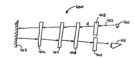
Refernng initially to Figure 4a, the present invention will be described with
reference to
a first embodiment of the invention which takes the form of a reflective type
SLM display
system generally designated by reference numeral 400. As illustrated in Figure
4a, system
400 includes an SLM 402 having a reflective backplane 403, a compensator cell
404,
polarizer 405, and an analyzer 406. Alternatively, in the same manner as
described above,
crossed polarizes 405 and analyzer 406 may be replaced with a polarizing beam
sputter.
System 400 is configured in a manner similar to that described above for
system 300 of
Figure 3a. That is, compensator cell 404 is positioned adjacent SLM 402. Also,
polarizes
405 is positioned to direct only horizontally linearly polarized light into
compensator cell
404. Similarly, analyzer 406 allows only vertically linearly polarized light
to pass through
it and into the viewing area after the light directed in to the system has
passed through
3(l compensator cell 404 and SLM 402 and been reelected back through SLM 402
and
compensator cell 40-I. However. in accordance with the invention. system 400
also
16
SUBSTITUTE SHEET (RULE 26)
CA 02321252 2000-08-14
WO 99/42898 PCT/US99/03347
includes a static quarter wave plate 408 positioned optically between
compensator cell 404 '
and polarizes 405 and analyzer 406.
As would be understood by those skilled in the art, SLM 402 may be made up of
an
array of any number of individually controllable pixels which are individually
switehable
between two states. For purposes of consistency, it will be assumed that each
pixel is
switched to its A state by applying a -+-~ VDC electric field through the
pixel and each
pixel is switched to its B state by applying a -5 VDC electric field through
the pixel. It
should be understood that the present invention is not limited to these
specific voltages
and would equally apply regardless of the voltages used to switch the pixels.
I 0 System 400 further includes a light source 410 for directing light into
the system in a
manner similar to that described above for Figures lb and lc. With this
configuration, light
source 410 directs light into polarizes 405 as indicated by arrow 412.
Polarizes 405 blocks
any vertically linearly polarized portions of the light from passing through
polarizes 405
an allows only horizontally linearly polarized portions of the light to pass
through
I 5 polarizes 405 into static quarter wave plate 408. This light passes
through static quarter
wave plate 408, compensator cell 404, and SLM 402 and is then reflected by
reflective
baekplane 403 back through SLM 402, compensator cell 404, and static wave
plate 408 to
analyzer 406 as illustrated in Figure 4a. Analyzer 406 then blocks any
horizontally
linearly polarized portions of the light and allows only vertically linearly
polarized
20 portions of the light to pass through it to a viewing area indicated by
viewer 416. Since
polarizes 405 blocks vertically linearly polarized light and analyzer 406
blocks
horizontally linearly polarized light. this type of system is referred to as
using crossed
polarizers.
For this embodiment and as described above for system 300, because the light
passes
25 through the SLM and the compensator cell twice in a reflective mode system,
the FLC
material of SLM 402 and compensator cell 404 are configured to act as quarter
wave plates
for a wavelength of S 10 nm. In this configuration, the FLC materials of both
SLM 402 and
compensator cell 404 are 900 nm thick and both have a tilt angle of 22.5
degrees. In this
specific embodiment, the buff axis of the SLM is positioned at a 22.5 degree
angle relative
30 to the horizontally linearly polarized light directed into the system.
Also, for this
embodiment, the buff axis of compensator cell 404 is positioned perpendicular
to the buff
17
SUBSTITUTE SHEET (RULE 26)
CA 02321252 2000-08-14
WO 99/42898 PCTlUS99/03347
axis of SLM 402. -
Although the buff ails Of the SLM is described as being positioned at 22.5
degrees
relative to the horizontally linearly polarized light directed into the
system, this is not a
requirement. In fact. this configuration works equally as well regardless of
the orientation
of the SLM buff axis relative to the horizontally linearly polarized light
directed inta the
system so lone as the buff axis of the compensator cell is oriented
perpendicular to the
buff axis of the SLM. This freedom in orienting the buff axis of the SLM
relative to the
horizontally linearly polarized light directed into the system makes this
overall system
easier to produce than other conventional systems because only the orientation
of the
I 0 SLM relative to the compensator cell must be precisely controlled.
The orientation of the static quarter wave plate relative to the horizontally
linearly
polarized light directed into the system is also important. Generally, static
quarter wave
plate 408 has a primary axis which is oriented at a 45 degree angle to the
horizontally
Linearly polarized light directed into the quarter wave plate.
15 Although the tilt angles of SLM 402 and compensator cell 404 are described
as being
22.5 degrees, this is not a requirement. The configuration described above for
this
embodiment works regardless of the tilt angle of the FLC material of the SLM
and the
compensator cell, but works best when the tilt angles of the two components
are the same.
Therefore, it should be understood that the present invention would equally
apply to
20 systems using SLMs and compensator cells having tilt angles other than 22.5
degrees.
With this configuration, the bright states obtained by the system remain
bright regardless
of the tilt angle used provided the tilt angles match. However, the use of
tilt angles in the
range of 22.5 to 25.5 degrees provides optimum dark state extinction, with the
choice of
tilt angle at the low end of the range providing best extinction over a narrow
range of
25 wavelengths centered on the wavelength for which the SLM and compensator
have
quarter-wave retardance and with the choice of tilt angle towards the upper
end of the
range providing good extinction over a more extended range of wavelength.
Increasing the
tilt angle past 25.5 degrees eventually reduces dark state extinction.
Now that the physical configuration of system 400 has been described, its
effect on
30 Eight directed into system 400 will be described. Figures 4b and 4c
illustrate the net result
that system 400 has on light directed in to the system. Fieure 4b shows the
results for
18
SUBSTITUTE SHEET (RULE 26)
CA 02321252 2000-08-14
WO 99/42898 PCT/US99/03347
Case 1 and 2 during which the compensator cell is in its B state and the SLM
is switched -
between the A state for Case 1 and the B state for Case 2. Case ! is indicated
by solid line
420 and Case 2 is indicated by dashed line 422. Figure 4c shows the results
for Case 3 and
4 during which the compensator cell is in its A state and the SLM is switched
between the
B state for Case 3 and the A state for Case 4. Case 3 is represented by solid
line 424 and
Case 4 is represented by dashed line 426. Cases I-4 correspond to Cases 1-4
for the
systems described above in the background.
As illustrated in Figures 4b and 4c. because of quarter wave plate 408 is
included in the
configuration of system 400, Cases 1 and 3 result in a dark pixel rather than
a bright pixel
1 (> and Cases 2 and 4 result in a bright pixel rather than a dark pixel. This
is the opposite of
the results described in the background. However, this inversion of the bright
and the dark
states may be compensated for in a variety of ways such as reversing the A and
the B
states for the SLM (i.e. using a -5 VDC to switch the pixel to the A state and
using a 5
VDC to switch the pixel to the B state). The important thing is that the
results of Cases 1
and 3 are identical and the results of Cases 2 and 4 are identical.
For system 400, static quarter wave plate 408 is preferably a readily
providable
achromatic quarter wave plate. The use of an achromatic static quarter wave
plate
provides the best results over a broad color spectrum because it flattens out
the curves 422
of Figure 4b and 426 of Figure 4c representing the bright states obtained by
Case 1 and
?4 Case 2. This flattening out of the curve improves the optical throughput of
system 400 by
increasing the amount of light which passes through the system for a given
pixel when the
combination of that pixel and the other elements are switched to produce a
bright state.
In one embodiment of the invention which reverses the bright and dark states
described
above for Figures 4a-c, parallel polarizers are used instead of crossed
pofarizers. Figure 5a-
?5 c illustrate a system 500 which utilizes parallel polarizers. As described
above for system
400, system 500 includes a SLM 502, a reflective backplane 503. a compensator
cell 504, a
polarizer 505, a static quarter wave plate 508, and a light source 510. Light
source 510
directs light into polarizer 505 which blocks any vertically linearly
polarized tight and
allows only horizontally linearly polarized light to pass through. This
horizontally
30 linearly polarized light then passes through and is acted upon by static
quarter wave plate
508, compensator cell 504, SLM 502, and reflective backplane 503 in the same
way as
19
SUBSTITUTE SHEET (RULE 26)
CA 02321252 2000-08-14
WO 99/42898 PCT/US99/03347
described above for Figure 4a. However, in this embodiment, polarizer 505 also
acts as the
analyzer for the system. This use of polarizer X05 for both the polarizer and
the analyzer
is what makes this system a parallel polarizer system.
In the configuration of Figure 5a, polarizer 505 acts as the analyzer by
blocking any
vertically linearly polarized light and allowing any horizontally linearly
polarized light to
pass into the viewing area. This is the opposite of the polarizations of light
blocked and
passed by analyzer 406 in system 400. This has the effect of reversing the
bright and dark
states of the system and results in the net effects illustrated in Figures 5b
and 5c. Figure
Sb shows the results for Case I and 2 during which the compensator cell is in
its B state
I 0 and the SLM is switched between the A state for Case 1 and the B state for
Case 2. Case
1 is indicated by solid line 520 and Case 2 is indicated by dashed line 522.
Figure 5c
shows the results for Case 3 and 4 during which the compensator cell is in its
A state and
the SLM is switched between the B state for Case 3 and the A state for Case 4.
Case 3 is
represented by solid line 524 and Case 4 is represented by dashed line 526.
Cases 1-4
t 5 correspond to Cases 1-4 for the systems described above in the background
and Cases 1-4
described above for Figure 4.
As clearly shown by Figures 5b and 5c, system 500 produces identical results,
that is, a
bright pixel for Case 1 and 3 as indicated by lines 520 and 524, respectively.
It also
produces identical results for Cases 2 and 4 as indicated by lines 522 and
526,
20 respectively. This configuration also produces very good results over the
entire
wavelength range from 400 nm to 700 nm. In fact, as illustrated by lines 522
and 526, this
configuration provides substantially uniform blockage of the entire range of
wavelengths of
the light that is directed into the spatial light modulator. Also, in both
Cases 1 and 3, a
large portion of the horizontally linearly polarized light passes through the
system for the
5 entire range of 400 nm to 700 nm. Since the point to adding the compensator
cell is to
increase the efficiency or brightness of the system, this arrangement
dramatically improves
the efficiency or brightness of system 500 over the complete wavelength range
when
compared to the system of Figure 1 b and 1 c which simply turns OFF the light
source
during the DC field-balancing time. This also substantially improves the
efficiency of the
30 system compared to system 300 of Figure 3 described above which does not
include the
static quarter wave plate. Furthermore, since essentially no light from the
light source
SUBSTITUTE SHEET (RULE 26)
CA 02321252 2000-08-14
WO 99142898 PCT/US99/03347
passes through the system to the viewing area when the elements are switched
to produce
a dark state as indicated by lines 522 and 526, this conf guration also
provides an excellent
contrast ratio.
In another embodiment similar to system 400 of Figure 4a, a birefringent
element may
be added to system 400 in order to provide results very similar to the results
obtained by
system 500 of Figure Sa. Using like reference numerals to represent like
components,
Figure 6 illustrates a system 600 including SLM 402. reflective backplane 403,
compensator cell 404, polarizes 405. analyzer 406, static quarter wave plate
408. and light
source 410. As described above for Figure 4, polarizes 405 and analyzer 406
are crossed
polarizers. However, in accordance with this embodiment of the invention,
system 600
further includes an additional birefringent element 612 which can be
positioned between
SLM 402 and compensator cell 404, as shown here, or alternately, can be
positioned
between compensator cell 404 and static quarter wave plate 408.
In this embodiment. birefringent element 612 is a commercially available
polycarbonate
film having a retardance of approximately one half of the wavelength of the
light for which
the system is optimized, for example a wavelength of 510 nm. Alternatively,
birefringent
element 612 may be any birefringent material capable of providing the desired
retardance
such as poly vinyl alcohol or any other optically clear birefringent material.
In this embodiment, the buff axes of SLM 402 and compensator cell 404 are
parallel to
20 one another and birefringent element 612 has a primary axis which is
oriented
perpendicular to the buff axis of both SLM 402 and compensator cell 404. As
describe
above for system 400, polarizes 405 directs horizontally linearly polarized
light into
quarter wave plate 408 and quarter wave plate 408 is oriented at a 45 degree
angle to the
horizontally linearly polarized light. SLM 402, compensator cell 404, and
birefringent
25 element 612 may be oriented in any way relative to quarter wave plate 408
so long as the
buff axes of SLM 402 and Compensator cell 404 are parallel to one another and
the
primary axis of birefringent element 612 is perpendicular to the buff axes of
SLM 402 and
compensator cell 404.
The addition of the birefringent element causes Case 1 and Case 3 for this
embodiment
3(? to result in a bright state in which the throughput varies only slightly
over the range of the
waveleneths similar to curves 520 and 524 of Figures Sb and Sc. Also. the
addition of the
21
SUBSTITUTE SHEET (RULE 26)
CA 02321252 2000-08-14
WO 99/42898 PCTIUS99/03347
birefringent element causes Case 2 and Case 4 for this embodiment to result in
a -
substantially more uniform dark state similar to lines 522 and 526 of Figures
5b and ~c.
This results in a system that is able to provide a high contrast ratio while
maintaining a
relatively high throughput for the entire wavelength range even though crossed
polarizers
are utilized.
Although the above described embodiments have been described as having the
static
quarter wave plate positioned between the polarizer and the compensator cell,
this is not a
requirement. Instead, the static quarter wave plate may be located between the
compensator cell and SLM and still remain within the scope of the invention.
In another embodiment, an off axis system may be utilized in order to provide
a
continuously viewable DC field-balanced reflective display system. Figures 7a
and 7b
illustrate one embodiment of an off axis display system 700. As illustrated in
Figures 7a
and 7b, system 700 includes a SLM 702, a ret7ective backplane 703, a
compensator cell
704, a polarizer 705, an analyzer 706, and a light source 710. In this
embodiment. the tight
I 5 is directed into the SLM at an angle and reflected back into a viewing
area indicated by
viewer 720 such that the light directed into the system only passes through
the
compensator cell once rather than passing through the compensator cetl twice
as described
above for the previously described embodiments.
Since the light only passes through compensator cell 704 once, the thickness
of
compensator cell 704 is configured to be twice the thickness of the SLM.
Generally, SLM
702 has a thickness which causes SLM 702 to act as a quarter wave plate when
switched
to its A state and compensator cell 704 has a thickness which causes it to act
as a half
wave plate when it is switched to its A state. Therefore. in the case in which
an FLC
material is used for both the SLM and compensator cell that has a
birefringence of 0.142,
5 the thickness FLC material for the SLM would be approximately 900 nm and the
thickness
of the FLC material for the compensator cell would be approximately 1800 nm.
Both
SLM 702 and compensator cell are configured to have substantially no effect on
the
polarization of the light passing through them when they are switched to their
B states.
For the configuration bein<~ described, polarizer 705 is configured to allow
only
horizontally linearly polarized light to be directed into the system. Analyzer
706 is
configured to allow only vertically linearly polarized light to pass into the
viewing area.
22
SUBSTITUTE SHEET (RULE 26)
CA 02321252 2000-08-14
WO 99/42898 PCT/US99/03347
Also, for this embodiment. the buff axis of compensator cell 704 is oriented
perpendicular -
to the buff axis of SLM 702 and the buff axis of SLIvI 702 is advantageously
oriented
parallel to horizontally linearly polarized light directed into the system.
Other orientations
of the buff axes are also effective provided that the SLM and compensator cell
buff axes
remain perpendicular to one another.
As described above for the previous embodiments, the off axis configuration
shown in
Figures 7a _and 7b provide identical results for Cases 1 and 3 and Cases 2 and
4. This
configuration also provides good results over a broad spectrum similar to the
results
illustrated in Figures 5b and 5c. Therefore, system 700 is also able to
provide a
continuously viewable system which more effectively utilizes light from the
light source
when compared to the conventional reflective systems illustrated in Figures Ib-
c and
Figure 3a.
Referring now to Figure 8, an on axis system 800 that utilizes a compensator
cell having
a thickness approximately twice the thickness of the SLM will be described. As
illustrated
in Figure 8, system 800 includes an SLM 802 having a reflective backplane 803,
a
compensator cell 804, a polarizes 805, and an analyzer 806. Alternatively, in
the same
manner as described above, crossed polarizes 805 and analyzer 806 may be
replaced with a
polarizing beam splitter.
System 800 is configured in a manner similar to that described above for
system 400 of
Figure 4a. That is, compensator cell 804 is positioned adjacent SLM 802. Also,
polarizes
805 is positioned to direct only horizontally linearly polarized light into
compensator cell
804. Similarly, analyzer 806 allows only vertically linearly polarized light
to pass through
it and into the viewing area after the light directed in to the system has
passed through
compensator cell 804 and SLM 802 and been reflected back through SLM 802 and
compensator cell 804. However, in accordance with this aspect of the
invention,
compensator cell 804 has a thickness and retardance that is substantially
different than that
of SLM 802. In the embodiment being described. compensator cell 804 has a
thickness and
retardance that is twice that of SLM 802.
System 800 further includes a light source 810 for directing light into the
system in a
manner similar to that described above for Figures 1 b and 1 c. With this
configuration, light
source 810 directs light into polarizes 805 as indicated by arrow 812.
Polarizes 805 blocks
23
SUBSTITUTE SHEET (RULE 26)
CA 02321252 2000-08-14
WO 99142898 PCTIU599/03347
any vertically linearly polarized portions of the light from passing through
polarizer 805
and allows only horizontally linearly polarized portions of the light to pass
through
polarizer 805 into compensator cell 804. This light passes through compensator
cell 804,
and SLM 802 and is then reflected by reflective backplane 803 back through SLM
802 and
compensator cell 804 to analyzer 806 as illustrated in Figure 8. Analyzer 306
then blocks
any horizontally linearly polarized portions of the light and allows only
vertically linearly
polarized portions of the light to pass through it to a viewing area indicated
by viewer 816.
Since polarizer 805 blocks vertically linearly polarized light and analyzer
806 blocks
horizontally linearly polarized light, this type of system is referred to as
using crossed
polarizers.
For this embodiment, the FLC material of SLM 802 is configured to act as a
quarter
wave plate for a wavelength of 510 nm. However, as mentioned above,
compensator cell
804 has a thickness and retardance that is twice that of SLM 802. Therefore.
compensator
cell 804 is configured to act as a half wave plate for a wavelength of 510 nm.
In this
configuration, the FLC material of SLM 802 is 900 nm thick and has a tilt
angle of 22.5
degrees. However, the FLC material of compensator cell 804 is 1800 nm thick
and has a
tilt angle of half that of the FLC material of SLM 802, that is, I I .25
degrees.
In the specific configuration being described, which is illustrated in Figure
9, the buff
axis of SLM 802 (indicated by dashed line 817) is aligned with or parallel
with the
horizontally linearly polarized light directed into the system. Also, for this
configuration,
the buff axis of compensator cell 804 (indicated by dashed line 8I8) is
positioned
perpendicular to the buff axis 817 of SLM 802. Alternatively, the system works
equally
well when configured with the buff axis 817 of the SLM aligned perpendicular
to the
horizontally polarized light and the buff axis 818 of the compensator cell
still
perpendicular to the buff axis of the SLM. This configuration is illustrated
in Figure 10a.
While these configurations may be preferred, other configurations still give
useful
performance characteristics. For example. with the buff axes 8I 7 and 818 of
the SLM and
compensator still perpendicular, the buff axes can be oriented at 45 de~~rees
to the
horizontally polarized incident light as illustrated in Figure lOb. In yet
another example.
~0 the buff axes 817 and 818 of the SLM and the compensator cell can be
parallel to each
other and aligned either both parallel to the horizontally polarized light. as
shown in Figure
24
SUBSTITUTE SHEET (RULE 26)
CA 02321252 2000-08-14
WO 99/42898 PCT/US99103347
IOc, or both perpendicular to the horizontally polarized light as shown in
Figure lOd. The -
same components can even be configured with both buff axis 817 and 818 being
oriented at
45 degrees relative to the horizontally polarized light, as illustrated in
Figure 10e.
Alternately, the buff axis 817 of the SLM can be oriented at 1 12.5 degrees
relative to
the horizontally polarized light with the FLC material of the SLM again having
a tilt angle
of 22.5 degrees). In this configuration, the buff axis 818 of the compensator
cell is oriented
11.25 degrees to the horizontally polarized light with the FLC material of the
compensator
cell again having a tilt angle of 11.25 degrees, or half that of the material
of the SLM. This
configuration is shown in Figure lOf.
I 0 Additionally, the orientations of Figure lOf can be oriented relative to
the vertically
polarized analyzer instead of relative to the horizontal polarizes without
changing the
results of the system. Finally, in still another specific configuration
illustrated in Figure
lOg, the buff axis of the SLM can be oriented 22.5 degrees from the
horizontally polarized
input light while the buff axis of the compensator cell is oriented nearly
parallel to the buff
I 5 axis of the SLM, at 168.75 degrees from the horizontally polarized input
light.
Although the tilt angles of SLM 802 and compensator cell 804 are described as
being
22.5 degrees and 11.25 degrees respectively for the above described
configurations, this is
not a requirement. The configurations described above for this embodiment work
for a
range of tilt angles, but work best when the tilt angle of the compensator
cell is half that of
20 the SLM. For example, in the case of the configuration of Figure lOf in
which the FLC
material of the SLM has a tilt angle different from 22.5 degrees, the SLM buff
axis is
preferably oriented at 90 degrees plus the SLM tilt angle from the
horizontally polarized
input light. Again, the compensator is preferably made from an FLC material
having half
the tilt of the SLM material, and the compensator buff axis of the compensator
cell is
S preferably oriented an angle equal to its tilt angle from the horizontally
polarized input
light. Therefore, it should be understood that the present invention would
equally apply
to systems using SLMs and compensator cells having tilt angles other than 22.5
degrees
and I 1.25 degrees respectively.
Although only a few specific examples of configurations having particular buff
angle
30 orientations have been identified above, the present invention is not
limited to these
specific examples. Instead. the present invention equally applies to a wide
variety of
SUBSTITUTE SHEET (RULE 26)
CA 02321252 2000-08-14
WO 99/42898 PCT/US99/03347
specific buff angle configurations. Generally, the configurations described
above. along
with many other useful configurations that result in a workable configuration,
may be
identified using the following equation.
P=:ESN+2C
S The equation identifies solutions that provide the desired display system
outputs.
That is. the solutions identified by the equation result in a system
configuration that
produces two relatively bright states and two relatively good dark states. The
equation is
used to determine the required buff angle P (measured in degrees from the
primary axis of
the polarized light directed into the system) for the SLM for any given
compensator buff
0 angle C (also measured in degrees from the polarized light directed into the
system) where
N is an integer.
The above identified equation assumes that the retardance of the FLC material
of the
SLM is a quarter wave for visible light and that the retardance of the
compensator cell is a
half wave for visible light. It also assumes that the tilt angle B of the FLC
material of the
I 5 compensator cell is half that of the tilt angle D of the FLC material of
the SLM. Generally,
when N is an odd integer, the bright states will be the most tolerant to
variations of the tilt
angles B and D, especially when B = D/2 is maintained. Alternatively, when N
is even, the
dark states will be most tolerant to the same variations of tilt angles B and
D. Better
arrangements also result when D = 22.5 degrees and B = 11.25 degrees.
20 In the configuration of Figure 9, the buff angle C of the compensator cell
is 90 degrees.
Therefore, when N is even, the buff angle P of the SLM is oriented a multiple
of 90 degrees
from the buff angle C of the compensator as required by the equation thus
making the buff
angles either perpendicular to or parallel to one another. Similarly, when N
is odd, the
equation results in an SLM buff angle that is rotated 45 degrees one way or
the other
2_~ relative to buff angle C of the compensator cell. All of these solutions
provide workable
configurations.
In the configuration of lOf, the compensator buff angle C is I I .25 decrees.
Therefore,
when N is equal to 2, the resulting SLM buff angle P is 1 12.5 degrees as
described above.
In the configuration of Figure 10 g, the compensator buff angle C is 168.7.
Therefore,
3O when N is equal to 1, the resulting SLM buff angle P is 382.5 degrees which
is the same as
22.5 degrees as described above for Figure I Of.
26
SUBSTITUTE SHEET (RULE 26)
CA 02321252 2000-08-14
WO 99142898 PCT/US99l03347
Now that the physical configuration of system 800 has been described. its
effect on
light directed into system 800 will be described. The use of the half wave
compensator cell
causes Case 1 and Case 3 for the embodiment described with reference to Figure
9 to result
in a bright state in which the throughput varies only slightly over the range
of the
wavelengths similar to curves 520 and 524 of Figures ~b and Sc. Also, for this
configuration that aligns the buff axis of the SLM with the horizontally
linearly polarized
light directed into the system, Case 2 and Case 4 result in a substantially
uniform dark
state similar to lines X22 and 526 of Figures Sb and Sc. This results in a
system that is able
to provide a high contrast ratio while maintaining a relatively high
throughput for the entire
wavelength range. The configuration with the buff axes rotated by 90 degrees
(i.e. the one
with the SLM buff axis oriented with the vertically polarized output light,
but the
compensator buff axis still perpendicular to the SLM buff axis) gives the
bright and dark
states of the same characteristics as the configuration of Figure 10(a). The
other
configurations generally give bright states with more throughput variation
over the
wavelength range and a less spectrally uniform dark state, but all provide the
contrast
reversal necessary for continuous viewing of the display system, and all
provide high
bright state throughput and a good dark state over at least a narrow range of
wavelengths.
Although system 800 has been described as using crossed potarizers, this is
not a
requirement of the invention. Instead, parallel polarizes may be utilized.
However, the
use of parallel polarizers reverses the light and dark states and results, for
the configuration
described with reference to Figure 10(a), in curves similar to those of
Figures 4b and 4c.
Although this configuration provides identical results for Cases 1 and 3 and
Cases 2 and 4,
it does not provide as good of a contrast ratio as system 800 using crossed
polarizers.
Now that the effect system 800 has on light directed into system 800 has been
?5 described, a variety of methods and arrangements for controlling the tilt
angle of
compensator cell 804 and SLM 802 will be described. As mentioned above for
system
800, it is important to maintain the tilt angle of the FLC material of
compensator cell 804
at half the tilt angle of the FLC material of SLM 802. This may be
accomplished in any
manner and still remain within the scope of the invention.
As is known in the art, the tilt angle of FLC materials is temperature
sensitive. That is,
for typical FLC materials, the tilt angle of the FLC material decreases as the
temperature of
27
SUBSTITUTE SHEET (RULE 26)
CA 02321252 2000-08-14
WO 99/42898 PCT/US99103347
the FLC material increases. Therefore, one approach to controlling the tilt
angle of the
FLC material of the compensator cell is to control the temperature of the
compensator cell.
With this approach, the temperature of the FLC material of the compensator
cell is
controlled at an elevated temperature so that its tilt angle is half that of
the tilt angle of the
FLC material of the SLM. Figure 11 illustrates a first embodiment of a heater
arrangement
designed in accordance with the invention for heating compensator cell 804 for
this
purpose.
In the embodiment shown in Figure 1 I, compensator cell 804 is made up of
three layers
of glass substrate 820, 822, and 824. Glass layers 820 and 822 have inner
faces 821 and
823 that respectively support electrodes 826 and 828. Electrodes 826 and 828
are
transparent electrodes, such as Indium-Tin-Oxide (ITO), that allow a voltage
to be applied
to control the state of compensator cell 804. The FLC material of the
compensator cell,
indicated by reference numeral 830, is sandwiched between ITO electrodes 826
and 828.
The third layer of glass, layer 824, has an inner surface 825 that supports a
layer 832 of
I 5 ITO material. Two electrical leads (not shown) are connected at opposite
ends of ITO
layer 832. These electrical leads are configured to provided electrical power
to ITO layer
832 which ITO layer 832 dissipates as heat. Preferably the electrical leads
are connected
to opposite edges of ITO layer 832 along the entire length of each edge. This
configuration
causes ITO layer 832 to be uniformly heated so that it heats the entire
compensator cell
including FLC material 830. Compensator cell 804 further includes a
temperature sensor
834 that is used to control the power provided to ITO layer 832. Therefore,
the
temperature of compensator cell 804 and FLC material 830 may be readily
controlled.
Although only one specific embodiment of a heater arrangement is described
above, it
should be understood that a wide variety of heating arrangements may be used
and still fall
5 within the scope of the invention. For example, although ITO layer 832 is
described as
being attached to the inner surface 825 of glass layer 824, it should be
understood that this
is not a requirement. Instead. ITO layer 832 may be attached to the outside
surface of
glass layer 824 or alternatively to any of the glass layers.
In another embodiment, a combined compensator cell and SLM panel
configuration,
where the SLM and compensator cell are maintained at substantially the same
temperature,
can be built by using different FLC materials in the display panel and in the
compensator
28
SUBSTITUTE SHEET (RULE 26)
CA 02321252 2000-08-14
WO 99/42898 PCT/US99/03347
cell. Figure 12 illustrates one embodiment of such a configuration. In this
embodiment. -
compensator cell 804 is attached directly to SLM 802. As described above.
compensator
cell 844 includes a heater arrangement. such as a layer of ITO material. that
is used to
maintain the temperature of the combination of compensator cell 804 and SLM
802 at a
particular temperature. Alternatively, a variety of other heater arrangements
may be used
to maintain compensator cell 804 and SLM 802 at a constant temperature.
Figure 13 illustrates the tilt angle vs. temperature characteristics of two
exemplary FLC
materials that may be used in the immediately above described configuration.
.4 high
temperature FLC material with the tilt angle vs. temperature characteristics
indicated by
l 0 curve 840 is used in SLM 802. A different, lower temperature FLC material
with tilt angle
vs. temperature characteristic indicated by curve 842 is used in the
compensator cell. For
reference, a curve showing half the tilt angle of the SLM FLC material of
curve 840 is
shown as curve 844. Both FLC materials illustrated are of the common type
having a
zero-tilt smectic A phase at temperatures above the ferroelectric smectic C
phase. In the
case of the material used in the SLM, the smectic A to smectic C phase
transition
temperature TAB has a value of about 90 °C (the temperature where the
tilt goes to zero),
while the material used in the compensator cell has a TAB value of about 55
°C.
As can be seen from Figure 13, the compensator tilt angle indicated by curve
842 has a
value equal to half the SLM FLC tilt indicated by curve 844 at a temperature
of about 40
°C (i.e. at the temperature where curve 842 and curve 844 intersect).
By physically
attaching the compensator cell to the display panel cell, as shown in Figure
12, it is
convenient to maintain them both at the same temperature. In a manner similar
to that
described above, the temperature of both cells together can be controlled, for
example, by
attaching a temperature sensor 834 to the combined compensator cell and SLM. A
resistive heater 846 may be attached to the back of the SLM and a temperature
control
servomechanism 848 may be used to supply electrical current to resistive
heater 846 in a
manner to maintain sensor 834 at a desired set-point temperature.
In the case of the exemplary FLC materials illustrated with respect to the
Figure 13,
setting the temperature-control set-point to 40 °C would result in
operation with the
3W compensator cell having half the SLM tilt, as desired for optimal operation
of system 800.
In general. the operation of such a temperature-controlled combined
compensator/ SLM can
29
SUBSTITUTE SHEET (RULE 26)
CA 02321252 2000-08-14
WO 99/42898 PCT/US99/03347
be achieved by fillin~~ the compensator cell with an FLC material having, at
some
temperature, a tilt angle substantially equal to half the tiff angle of the
FLC material used in
the SLM at that temperature. Specifically, this can be accomplished by filling
the
compensator cell with an FLC material having a TAB suitably lower than the TAB
of the
SLM FLC material.
Another method of controlling the tilt angle of an FLC material is to control
the drive
voltage used to switch and maintain the FLC material in its A and B-states. As
described
above in the background. FLC materials are switched to and maintained in their
A and B
states by establishing and maintaining certain drive voltages through the
layers of FLC
I c) materials. Generally, lower drive voltages result in lower tilt angles
and higher voltages
result in larger tilt angles. Figure 14 illustrates how the combination of
drive voltage and
temperature effect the tilt angle of a typical FLC material.
Because the tilt angle of FLC material varies in a predictable way as the
drive voltage
used to maintain the FLC material in their A and B states. the tilt angle of
compensator cell
I 5 804 and SLM 802 may be controlled by applying the appropriate drive
voltages. In a
manner similar to that described above for the temperature controlling
approach, the drive
voltages for the compensator cell and the SLM may be controlled such that the
resulting
tilt angle of the compensator cell is half that of the SLM. However, one
problem with this
approach is that the switching speed of the FLC material is also effected by
the drive
20 voltage used to establish and maintain the FLC material in the desired
state.
In order to overcome this potential switching speed problem, the drive voltage
used to
establish and maintain the FLC material in the desired state may include a
leading edge
spike. Figure 15 illustrates a drive voltage waveform 850 including a leading
edge spike 852
that may be used to overcome the reduction of switching speed which may occur
when a
S low voltage is used for the drive voltage in order to reduce the tilt angle
of the compensator
cell. In Figure 15, Vhoa ~s a low voltage, e.g. 0.5 - 2.0 Volts. which is
adjusted to tune the
FLC tilt angle of compensator cell 804 to exactly half of the tilt angle of
the FLC in
associated SLM 802. f lowever, uhotd is too low a voltage to cause the FLC ot~
compensator cell 804 to switch quickly between its two states. Vpeak Is a high
voltage, e.g.
3e) 6 Volts, which drives the FLC material of compensator cell 804 quickly
between its two
states. If left on the compensator, Vpeak would produce a tilt angle that is
much too high.
SUBSTITUTE SKEET (RULE 26)
CA 02321252 2000-08-14
WO 99/42898 PCT/US99/03347
Thus. the applied voltage is reduced from ~'Pcak to unota after the fast
switching has been -
accomplished.
Any combination of the above described two approaches may be used to
controlling the
tilt angle of the FLC material of the compensator cell or the combination of
the
compensator cell and the SLM. For example. relatively low drive voltages may
be used to
drive the compensator cell while the compensator cell is maintained at an
elevated
temperature compared to the SLM. The combination of these two- approaches may
be
used to cause the FLC material of the compensator cell to have a tilt angle
half that of the
FLC material of the SLM.
1_Q It may be desirable to implement an SLM plus compensator display system
according
to one of the above configurations where it is not necessary to know exactly
at what
voltage or temperature the desired tilt angle of the FLC compensator material
is obtained.
This can be accomplished with a servo system that detects the display system
dark state
intensities and how these intensities vary with compensator drive voltage.
Given the
~ 5 variation of compensator tilt angle with voltage shown in an exemplary way
in Figure 14,
the display system dark state output intensity should vary with compensator
cell drive
voltage as shown in Figure 16 when the pixel state is such that a positive
compensator-cell
drive voltage produces a display system dark state.
As can be seen in Figure 16, there is an optimum compensator drive voltage
which
20 produces a minimum display system output intensity, indicated by point 860.
This is the
drive voltage which results in the compensator cell optic axis orientation
most nearly
approximating that required by the configurations described above. If the
display system
happened not to be at this optimum point. the needed corrective action could
be
determined as follows. Suppose the system output intensity had the non-minimum
level
2~ indicated by dashed line 862. Suppose further that a slight increase in the
compensator
drive voltage caused a further increase to the display system output intensity
Level. Then,
the system must be operating near point 864 indicated in Figure 16. This means
that the
system contrast could be improved if the compensator cell tilt were reduced by
reducing
the compensator drive voltage. Alternately, suppose that a slight increase in
the
30 compensator drive voltage caused a decrca.se to the display system output
intensity.
Then, the system must be operating near point 866 indicated in Figure 16. This
means
31
SUBSTITUTE SHEET (RULE 26)
CA 02321252 2000-08-14
WO 99/42898 PCT/EJS99/03347
that the system contrast could be improved if the compensator cell tilt were
increased by -
increasing the compensator drive voltage.
A servomechanism that can automatically keep the compensator cell tilt at its
optimum
value is shown in Figure 18. In this embodiment. the pixel array. indicated by
region 870
in Figure 17, of SLM 802 has an adjacent or surrounding apron area 872. Apron
area 872
functions in exactly the same way that the pixels function, but is not part of
the desired
image. However, the apron area is driven so that it shouid always produce a
dark output
state, even as the compensator cell is switched to accomplish DC balancing of
both the
pixel area and the apron area. Display system output light from this apron
area is imaged
I 0 onto a photodetector 880 (shown in Figure I S) that provides an input
signal 882 for the
servomechanism. The compensator cell is driven from a signal source 884 that
adds a small
high-frequency dither signal 886 to a lower-frequency alternating polarity
drive signal 888.
For example, if the display system were performing DC balance such that an
image data
frame and an inverse image data frame were displayed on the SLM in a period
having a
total duration of 1/60 of a second, the compensator cell would be cycling at a
rate of 60
Hz. The lower-frequency compensator drive signal 888 would be a 60 Hz square
wave
having an amplitude of, for example, 1.5 V. The dither signal 886 could then
be, for
example, a 2400 Hz square wave with an amplitude of 0.2 V.
When the apron drive voltage is such that the positive portion of the
compensator-cell
square-wave drive waveform should produce a display system output dark state,
the
output of the photodetector is detected by a phase-sensitive detector or lock-
in amplifier
890 whose reference input is driven by the dither signal 886. As is well known
in the art,
this type of detection scheme produces a positive output when the input signal
(the
photodetector output) is in phase with the reference signal (the compensator
dither signal)
and a negative output when the input signal is out of phase with the reference
signal. This
output signal can be low-pass filtered using low pass filter 892 to remove
unwanted noise.
The sign of the lock-in amplifier output signal indicates whether the
compensator tilt
angle is too much or too little, and the magnitude of the signal indicates the
degree of error.
The servomechanism feeds this Lock-in amplifier output signal back to control
the level of
the compensator cell drive voltage in such a way as to reduce the error signal
to zero. If
the error signal is positive (dark-state output intensity increasing with
compensator drive
32
SUBSTITUTE SHEET (RULE 26)
CA 02321252 2000-08-14
WO 99/42898 PCT/US99103347
voltage), then the amplitude of the lower-frequency compensator drive voltage
is reduced. -
If the error signal is negative (dark-state output intensity decreasing with
compensator
drive voltage), then the amplitude of the lower-frequency compensator drive
voltage in
increased.
The description above characterizes the performance of the servo system during
the
phase when the apron (or dark pixels) are driven such that a positive
compensator cell
drive voltage produces a display system output dark state. The servo system
operates
similarly during the other phase when the compensator is driven with a
negative voltage,
but the feedback sense is reversed to accommodate the fact that reversal of
the change in
lO output intensity with variation of compensator drive voltage. The
servomechanism need
not constrain the positive and negative compensator drive voltages to be equal
in
magnitude; different magnitudes can be used to correct for small compensator
buff axis
misorientations that arise, for example, as a result of non-zero manufacturing
assembly
tolerances.
I 5 The servomechanism was described above as operating on the compensator
cell drive
voltage. The servo could equally well operate on the compensator temperature.
In the
case of operating on temperature, if the lock-in detected that the compensator
tilt was
larger than optimum, a feedback signal could be supplied to the compensator
temperature
controller that would cause the compensator temperature to be increased, and
vice versa.
Although only certain specific embodiments of the present invention have been
described in detail, it should be understood that the present invention may be
embodied in
many other specific forms without departing from the spirit or scope of the
invention. For
example, although the systems have been described above as using horizontally
linearly
polarized light as the initial input light polarization, this is not a
requirement. Instead, it
25 should be understood that the initial input light polarization may
alternatively be vertically
linearly polarized light. Also, although only two specific examples of how to
control the
tilt angle of the FLC material of the compensator cell using heating and
reduced drive
voltage have been described, it should be understood that the present
invention is not
limited to these specific examples. Instead, any combination of these two
approaches, or
3W any other method of controlling the tilt angle, may be utilized and still
fail within the scope
of the invention. Therefore, the present examples are to be considered as
illustrative and
33
SUBSTITUTE SHEET (RULE 26)
CA 02321252 2000-08-14
WO 99/42898 PCT/US99/03347
not restrictive. and the invention is not to be limited to the details given
herein. but rnay be -
modified within the scope of the appended claims.
34
SUBSTITUTE SHEET (RULE 26)