Note: Descriptions are shown in the official language in which they were submitted.
CA 02321370 2003-O1-31
GRAPHIC ACCELERATOR WITH INTERPOLATE FUNCTION
The present invention relates to a graphic accelerator for performing a high-
speed image display.
With reference to Fig. 16, image information which has been processed in a
conventional two dimensional graphic accelerator will be described. In Fig.
16,
RGB (x,y) represents R color information, G color information, and B color
information at a pixel location (x,y).
The conventional graphic accelerator thus processes R/GB color information
of a few bits each for each pixel which is the basic unit constituting a
screen to be
displayed. R/GB color information of each pixel is temporarily stored in an
external image memory region, read out therefrom and processed as data.
In a 3D graphic accelerator (3D: three dimension) employing Z buffering
method, information to be processed includes depth information (Z value) and
transparency information (a value) given for each pixel, texture, which is
pattern
data to be pasted on to a polygon, and so on, in addition to R/GB color
information.
Similarly, the information is temporarily stored in an external image memory
region, read out therefrom and processed as data.
The size of a screen (the number of pixels) has been increasing recently and
the required image memory capacity has also increased.
In the conventional graphic accelerator, however, when the amount of data to
be stored in the image memory increases, the amount of data to be transferred
between the graphic accelerator and the image memory increases causing an
undesirable effect on the process speed. Particularly in the graphic
accelerator
capable of processing three dimensional images, as the required image data
memory
capacity increases and data to be processed is considerable, the improvement
in
image-forming process performance is
-1-
CA 02321370 2003-O1-31
hard to achieve.
For the achievement of high-speed processing, the graphic
accelerator and the image memory are required to be incorporated in one
chip formed on the san~:e semiconductor substrate. The increase in image
memory capacity required hampers such a requirement.
SUMMARY OF THE INVENTION
Hence, the present invention provides a graphic accelerator capable
of processing image data at high speed by suppressing the increase in
image memory capacity.
A graphic accelerator according to one aspect of the present invention
generates display data based on data stored in an image memory and
includes; a storage control unit receiving a plurality of pixels each having
three types of color information such as RGB, deleting one of three types of
color information in each pixel, and storing color information of the
plurality of pixels in the image memory such that the color information
includes a pixel having two types of color information except first type color
information among three types of color information and a pixel having two
types of color information except second type color information different
from the first type color information among three types of color information;
and an interpolation process unit interpolating color information deleted by
the storage control unit with a pixel including deleted color information
among the plurality of pixels stored in the image memory, for each of the
plurality of pixels stored in the image memory. The graphic accelerator
supplies display data as an output according to the plurality of pixels stored
in the image memory and interpolation result of the interpolation process
unit.
According to the graphic accelerator described above, one type of
color information among three types of color information is deleted and two
types of color information are stored in the image memory for each pixel.
Then, deleted color information is interpolated with a pixel which is stored
in the image memory and includes deleted color information. Thus, even
with a larger screen, information to be stored in the image memory can be
reduced. As a result, the amount of data to be transferred between the
-2-
CA 02321370 2003-O1-31
image memory and the graphic accelerator can be reduced. Hence, more
rapid image processing can be achieved. In addition, as the image memory
requirement is decreased, the image memory and the graphic accelerator
can be incorporated in a single chip.
Preferably, the storage control unit stores two types of color
information except the first type color information among the three types of
color information in the image memory for each of the plurality of pixels
arranged in a direction of even scan lines, and stores two types of color
information except the second type color information among the three types
of color information in the image memory for each of the plurality of pixels
arranged in a direction of odd scan lines.
According to the above described graphic accelerator, capacity of
image memory can be reduced to two-thirds of the capacity of conventional
device. In addition, as the process is performed in the direction of scan
line, the interpolation process can be readily embodied in a hardware and a
compact circuit structure can be achieved.
Preferably, the storage control unit stores two types of color
information except the first type color information among the three types of
color information in the image memory for each of a first plurality of pixels
arranged as a matrix and included in the plurality of pixels, and stores two
types of color information except the second type color information among
the three types of color information in the image memory for each of a
remaining second plurality of pixels included in the plurality of pixels.
According to the above-described graphic accelerator, image memory
capacity can be reduced to two-thirds of the capacity of conventional device.
Preferably, the storage control unit divides the plurality of pixels into
a plurality of blocks, deletes color information so .that the plurality of
blocks
each include a first type pixel not having the first type color information of
the three types of color information and a second type pixel not having the
second type color information of the three types of color information, and
the interpolation process unit interpolates the deleted color information of a
pixel to be interpolated with a pixel having the deleted color information
and included in the same block as the pixel to be interpolated.
-3-
CA 02321370 2003-O1-31
According to the above-described graphic accelerator, the plurality of
pixels are divided into blocks and one of three types of color information is
deleted for one pixel, and another of three types of color information is
deleted for another pixel in each block, and the resulting color information
is
stored in the image memory. Interpolation is performed block-wise. Thus,
the image memory capacity can be reduced to two-thirds of the capacity of
conventional device.
Preferably, the storage control unit deletes color information such
that the plurality of pixels to be output include a first type pixel not
having
B color information among the three types of color information, a second
type pixel not having R color information among the three types of color
information, and a third type pixel not having G color information among
the three types of color information.
According to the above-described graphic accelerator, R color
information is deleted for one pixel, G color information is deleted for
another pixel, and B color information is deleted for still another pixel.
Thus, image memory capacity can be reduced to two-thirds of the capacity
of the conventional device.
Preferably, each of the plurality of pixels written into the image
memory includes the same color information. Particularly, each of the
plurality of pixels written into the image memory includes G color
information.
According to the above-described graphic accelerator, display results
similar to an original image can be obtained when G color information is
not deleted.
Particularly, the plurality of pixels are arranged in the image
memory such that a first line in which all pixels arranged in the scan
direction of the screen are the first type pixels, a second line which is next
to the first line and in which all pixels arranged in the scan direction of
the
screen are the second type pixels, and a third line which is next to the
second line and in which all pixels arranged in the scan direction of the
screen are the third type pixels are repeatedly arranged.
According to the above-described graphic accelerator; first color
-4-
CA 02321370 2003-04-30
information is deleted from three types of color information with regard to
pixels in
(3N+1)th scan lines, second color information is deleted from three types of
color
information with regard to pixels in (3N+2)th scan lines, and third color
information
is deleted from three types of color information with regard to (3N+3)th scan
lines.
Thus, the image memory capacity can be reduced to two-thirds of the
conventional
device capacity. In addition, as the process is performed in the direction of
scan
line, interpolation process can be readily embodied in a hardware and a
compact
circuit structure can be obtained.
A graphic accelerator according to another aspect of the present invention,
which is claimed in Canadian Divisional Application Serial No. 2,417,468,
generates display data based on data stored in an image memory and includes; a
storage control unit receiving a plurality of pixels each having color
information and
Z value information designating depth, dividing the plurality of pixels into a
plurality of blocks, updating shared Z value information and storing the
resulting
information in the image memory on each block basis, comparing Z value
information of a pixel and shared Z value information stored in the image
memory
on each block basis, and updating color information of the pixel and storing
the
resulting information in the image memory according to a hidden surface
removal
process, and a circuit supplying the display data as an output employing the
plurality of pixels stored in the image memory.
Preferably, each of the plurality of pixels to be supplied as an input further
includes a value information designating transparency. The storage control
unit
updates shared a value information and stores the resulting information in the
image
memory on each block basis, compares Z value information of the pixel and
shared
Z value information stored in the image memory, updates color information of
the
pixel according to the hidden surface removal process and an alpha blending
process based on the shared a value stored in the image memory and stores the
resulting information in the image memory.
-5-
CA 02321370 2003-O1-31
Particularly, the image memory includes a Z buffer storing Z value
information shared on each block basis and a frame buffer storing color
information
of each of the plurality of pixels and a value information
- Sa -
CA 02321370 2003-04-30
shared on each block basis.
According to the above-described graphic accelerator, the plurality of pixels
are
divided into blocks and each depth information Z and transparency information
a are
shared by pixels in each block. Thus, the image memory capacity of the Z
buffer and the
frame buffer can be significantly reduced compared with a conventional
approach where
depth information Z and transparency information a are stored for every pixel.
Hence,
more rapid image processing can be achieved. In addition, as there is a
reduction of image
memory required, the image memory and the graphic accelerator can be
incorporated in a
single chip.
The foregoing and other features, aspects and advantages of the present
invention
will become more apparent from the following detailed description of the
present invention
when taken in conjunction with the accompanying drawings.
BRIEF DESCRIPTION OF THE DRAWINGS
Fig. 1 is a diagram showing an outline of a structure of a graphic accelerator
according to the first embodiment of the present invention;
Fig. 2 is a conceptual diagram shown for describing a storing scheme according
to
the first embodiment of the present invention;
Figs. 3A to 3F are conceptual diagrams shown for describing information to be
stored in a frame buffer 106 according to the first embodiment of the present
invention ;
Fig. 4 is a diagram showing a structure of a specific example of graphic
accelerator
100;
Fig. 5 is a flow chart showing an example of a specific processing procedure
in an
interpolation process unit 114;
Fig. 6 is a conceptual diagram shown for describing data storing scheme
according
to the second embodiment of the present invention;
Figs. 7A to 7F are conceptual diagrams shown for describing information to be
stored in a frame buffer 106 according to the second embodiment of the present
invention;
Fig. 8 is a conceptual diagram shown for describing data storing scheme
according
to the third embodiment of the present invention;
-6-
CA 02321370 2000-09-27
Figs. 9A to 9D are conceptual diagrams shown for describing
information to be stored in frame buffer 106 according to the third
embodiment of the present invention;
Fig. 10 is a flow chart showing an example of a specific processing
procedure in interpolation process unit 114;
Fig. 11 is a conceptual diagram shown for describing information of
pixel information to be stored in frame buffer 106 according to the fourth
embodiment of the present invention;
Fig. 12 is a diagram showing a structure of a graphic accelerator 200
according to the fifth embodiment of the present invention;
Figs. 13A to 13C are conceptual diagrams shown for describing
information to be stored in the frame buffer and the Z buffer;
Fig. 14 is a conceptual diagram shown for describing a storing
scheme according to the fifth embodiment of the present invention;
Fig. 15 is a conceptual diagram shown for describing information to
be stored in frame buffer 106 and Z buffer 206 according to the fifth
embodiment of the present invention;
Fig. 16 is a conceptual diagram showing image information to be
processed in the conventional two-dimensional graphic accelerator.
DESCRIPTION OF THE PREFERRED EMBODIMENTS
The detailed description of the embodiments of the present invention
will be provided hereinbelow with reference to the drawings. In the
drawings, the same or a corresponding element will be denoted by the same
reference character and the description thereof will not be repeated.
First Embodiment
With reference to Fig. 1, a graphic accelerator according to the first
embodiment of the present invention will be described. A graphic
accelerator 100 includes a image-forming data decode unit 101, an image
memory control unit 102, an screen data generation unit 103 and screen
display control unit 104. Graphic accelerator 100 is built in a personal
computer, home game tool, or the like, processes image-forming data
transmitted from an external CPU or the like and supplies display data as
an output to a display device 105.
_7_
CA 02321370 2000-09-27
Image-forming data decode unit 101 receives a command for
performing image-forming process (draw the lineldraw the rectangle, for
example) and decodes image-forming data into an image.
Image memory control unit 102 performs control for writing the
output of image-forming data decode unit 101 into a frame buffer 106 and
reading out information stored in frame buffer 106.
Screen data generation unit 103 restores (interpolates) color
information according to a storing scheme and generates screen data based
on data read from frame buffer 106.
Screen display control unit 104 performs processes such as digital-
analog conversion on the output from screen data generation unit 103 for
display at a corresponding display device 105 and outputs the result to
display device 105.
Next, the data storing scheme and the data decoding (interpolating)
scheme tolfrom frame buffer 106 according to the first embodiment of the
present invention will be described. Here, the description is given on three
types of color information R/GB constituting a pixel.
The storing scheme according to the first embodiment of the present
invention will be described with reference to Fig. 2. In Fig. 2, character P
(x, y) represents a pixel on a coordinate (x, y) in a screen 1. In the first
embodiment of the present invention, screen 1 constituted of a plurality of
pixels P (x, y) arranged as shown in Fig 2 are divided into groups of odd
scan lines (hatched portion) and even scan lines (non-hatched portion)
across the direction of y axis (direction of scan line). Pixels P (0,0), P
(1,0),
..., belong to odd scan line group GR1, whereas pixels P (0,1), P (1,1), ...,
belong to even scan line group GR2.
With reference to Fig. 3, information to be stored into frame buffer
106 for each of these groups is described. In Figs. 3A to 3F, character F (x,
y) represents a storage region in frame buffer 106 associated with pixel P (x,
y). Character R (x, y), character G (x, y) and character B (x, y) represent R
color information, G color information and B color information of pixel P (x,
y), respectively.
In the first embodiment of the present invention, combination of color
_g_
CA 02321370 2000-09-27
information to be stored in frame buffer 106 differs from odd scan lines (Fig.
3A, 3B, 3E and 3F) to even scan lines (Fig. 3C and 3D).
For example, from RIGS color information, G color information and
B color information are stored and R color information is not stored with
regard to a pixel in an odd scan line. Then, with regard to a pixel in an
even scan line, R color information and G color information are stored and
B color information is not stored.
Next, data interpolating scheme in screen data generation unit 103
will be described. For the display of image, three types of color
information R/G/B are required: Hence, in the first embodiment of the
present invention, with regard to a pixel arranged in the odd scan line
(even scan line), when corresponding color information is to be read out
from the frame buffer, color information that has not been stored is
interpolated with color information of a pixel in an adjacent even~scan line
(odd scan line). Here, color information is shared between the pixel in the
odd scan line and the pixel in the even scan line located next to each other.
For example, with regard to pixel P (1, 0) in an odd scan line, G color
information G (1, 0) and B color information B (1, 0) have been stored in
storage region F (1, 0) of frame buffer 106, while R color information has
not been stored. Thus, R color information of an adjacent even scan line,
for example, R (1, 1) of pixel P (l, 1) is treated as R color information of
the
pixel P (1, 0) and used for interpolation. With regard to pixel P (1, 1) in an
even scan line, R color information R (1, 1) and G color information G (1, 1)
have been stored in storage region F (1, 1) of frame buffer 106, while B color
information has not been stored. Thus, B color information of an adjacent
odd scan line, for example, B (1, 2) of pixel P (1, 2) is treated as B color
information of the pixel P (1, 1) and used for interpolation.
A specific example of graphic accelerator 100 achieving such an
operation will be described with reference to Fig. 4. The graphic
accelerator shown in Fig. 4 includes an image-forming command decode
process unit 110 receiving image-forming data to decode a command, a color
information deletion process unit 112 deleting color information not to be
stored in frame buffer 106 from image-forming data according to the storing
_g_
CA 02321370 2000-09-27
scheme described above, image memory control unit 102, an interpolation
process unit 114 and a screen display control unit 104. Image-forming
command decode process unit 110 and color information deletion process
unit 112 are included in image-forming data decode unit 101.
Interpolation process unit 114 is included in screen data generation unit
103.
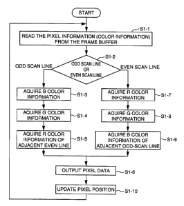
An example of a specific processing procedure in interpolation
process unit 114 is shown in Fig. 5. At step S1-1, pixel information (color
information) is read out from frame buffer 106. Stored information can be
read out along the direction of scan line (raster direction) of display device
105 on which the display is to be shown, or stored information
corresponding to two adjacent pixels in longitudinal direction can be read
out, or stored information can be read out block by block.
At step S1-2, it is determined whether a pixel to be interpolated is
arranged in an odd scan line or in an even scan line. When the pixel is
arranged in an odd scan line, the process proceeds to step S1-3 and
corresponding B color information (step S1-3) and G color information (step
S1-4) are acquired from read-out pixel information. Further, the
interpolation is performed with R color information of a pixel in an adjacent
even scan line (step S1-5). At step S1-6, acquired R, G, and B color
information are output into screen display control unit 104.
When the pixel to be interpolated is determined to be arranged in an
even scan line at step S1-2, the process proceeds to step S1-? and
corresponding R color information (step S1-?) and G color information (step
S1-8) are acquired from read-out pixel information. Further, the
interpolation is performed with B color information of a pixel in an adjacent
odd scan line (step S1-9). At step S1-6, acquired R, G, and B color
information are output into screen display control unit 104. After the
completion of step S1-6, the process proceeds to step S1-10 and the position
of the pixel to be interpolated is updated.
Here, stored information of pixel P (1, 1) is used for pixel P (1, 0). In
other words, in the case described above, data of an adjacent scan line is
employed as it is for the interpolation of color information not stored. The
-10-
r
CA 02321370 2003-O1-31
interpolation process is not limited thereto. For example, for the
interpolation of B color information of pixel P (1, 1), the interpolation data
can be obtained as an average of B color information of adjacent pixels P (0,
0), P (2, 0), P (0, 2), P (2, 2).
The combination of color to be stored in frame buffer lOf is not
limited to those described above. Any color information can be deleted.
In addition, when the reproducibility of the color is considered, G
color information is not shared by pixels and G color information is stored
(in an associated frame buffer) for each pixel.
This is because the quality of the display is greatly affected when G color
information is shared among pixels. G color information has a big effect
on a luminance component (Y component) of displayed color and sight of the
human is more sensitive to the change in luminance component than to the
color difference information (V information and U information).
Expressions (1)-(3) shown below demonstrate the significant effect of G
color information on the luminance component of the color. Expressions
(1)-(3) are for performing color space conversion from RGB to YUV.
Y = 0.2998 - 0.5876 + 0.1148 ... (1)
V = Cb = - 0.16878 - 0.33136 + 0.5008 ... (2)
U = Cr = 0.5008 - 0.41876 - 0.08138 ... (3)
In the above expression representing luminance information Y, the
factor of the term corresponding to the G component (0.587) is larger than
the factor of the R or B component. Thus, it is proved that the G
component has a great effect on luminance information.
Thus, G color component is not shared by pixels and R or B
component is shared. Thus, the display result will become close to the
original image.
According to this process, two kinds of color information are stored in
frame buffer 106 for each of the pixels on the screen. Hence, the required
capacity of the frame buffer can be reduced to two-thirds of that of the
conventional graphic accelerator storing RIGIB color information for each
pixel, without significantly degrading the quality of the display. .Thus, the
amount of data to be transferred to/from frame buffer 106 can be reduced.
-11-
CA 02321370 2000-09-27
Hence, still faster data process can be achieved. When frame buffer 106 is
connected on the substrate, the number of pins and interconnections can be
reduced.
Though in the drawing, frame buffer 106 is arranged in a different
region from that of graphic accelerator 100, these can be formed on the
same semiconductor substrate.
In addition, though in the above description the graphic accelerator
processing the two dimensional image data has been described, a graphic
accelerator capable of processing three dimensional image data and
processing transparency information a and depth information Z in addition
to R/GIB color information can be applied.
Second Embodiment
A data storing scheme in a graphic accelerator according to the
second embodiment of the present invention will be described. In the
second embodiment of the present invention, a matrix-like group division is
performed as shown in Fig. 6 (Here, the term "matrix" include a checker).
To be specific, pixels adjacent to each other belong to different groups. For
example, when pixel (1, 1) belongs to one group GR1 (hatched), pixels P (1,
0), P (0, 1), P (2, 1), and P (1, 2) adjacent to pixel P (1, 1) belong to
another
group GR2 (non-hatched).
Next, with reference to Figs. 7A-7F, information stored to frame
buffer 106 for each of these groups will be described. In the second
embodiment of the present invention, the combination of color information
to be stored in frame buffer 106 is changed for every group as shown in Figs.
7A-?F.
For example, with regard to pixels (P (0, 0), P (1, 1), P (2, 0), ...)
which belong to group GR1, G color information and B color information
among RIG/B color information are stored and R color information is not
stored. With regard to pixels (P (0, 1), P (1, 0), P (2, 1), ...) which belong
to
group GR2, R color information and G color information are stored and B
color information is not stored.
Next, a data interpolating scheme in screen data generation unit 103
of the second embodiment of the present invention will be described. In
-12-
CA 02321370 2000-09-27
the second embodiment of the present invention, with regard to pixels
which belong to group GR1 (GR2), color information that has not been
stored is interpolated by color information of a pixel which belongs to group
GR2 (GRl) when corresponding pixel information is read out from the
frame buffer. Here, interpolation of the color information is performed
using color information of adjacent pixels.
For example, with regard to pixel P (1, 1) that belongs to group GR1,
G color information G (1, 1) and B color information B (1, 1) have been
stored in frame buffer 106, whereas R color information has not been stored.
Hence, R color information of a pixel that belongs to group GR2, for
example, R color information R (1, 0) of pixel P (1, 0) is treated as R color
information of pixel P (1, 1) and is used for interpolation.
By replacing the odd scan line and even scan line in the flow chart of
Fig. 5 with group G1 and G2, respectively, a specific interpolation process
can be shown.
In the example described above, color information of an adjacent
pixel in a lateral direction is employed for interpolation of color
information
not stored. The interpolation process is not limited to this. For example,
an average of the color information of the pixels located right and left to
the
pixel of interest can be used. In this case, the same effect can be obtained.
In addition, an average of B color information (0, 0) of pixel P (0, 0)
and B color information B (0, 2) of pixel P (0, 2) can be used for the
interpolation of B color information of pixel P (0, 1). In other words, an
average of information of adjacent pixels located above and below the pixel
of interest can be used. The same effect can be obtained also in this case.
In addition, for the interpolation of R color information of pixel P (1,
1), average of R color information of pixels P (1, 0), P (0, 1), P (1, 2), P
(2, 1)
can be used. In other words, an average of information of adjacent pixels
located above, below, right and left to the pixel of interest can be used.
The same effect can be obtained again in this way.
The combination of colors to be stored in frame buffer 106 is not
limited to those described above and any color information can be deleted.
Through this process, two kinds of color information are stored in
-13-
CA 02321370 2000-09-27
frame buffer 106 for each of all pixels on the screen. Hence, the required
capacity of the frame buffer can be reduced to two-thirds of that of the
conventional graphic accelerator storing R/G/B color information for each
pixel without significantly degrading the quality of the display.
Thus, the amount of data to be transferred tolfrom frame buffer 106
can be reduced. Thus, still faster data process can be achieved. In
addition, frame buffer 106 can be formed in the same semiconductor
substrate as one-chip.
In the above description, the graphic accelerator processing two
dimensional image data is described. The described process can be applied
to a graphic accelerator capable of three-dimensional data processing and
processing transparency information a and depth information Z in addition
to R/G/B color information.
Third Embodiment
Next, data storing scheme in a graphic accelerator according to the
third embodiment of the present invention will be described. In the third
embodiment of the present invention, screen 1 is divided into rectangular
blocks as shown in Fig. 8 as a unit of the color information sharing.
In Fig. 8, the size of one block is two pixels by two pixels. Pixels P
(0, 0), P (1, 0), P (0, 1), P (1, 1) belong to one block and pixels P (2, 0),
P (3,
0), P (2, 1), P (3, 1) belong to another block.
With reference to Figs. 9A to 9D, information to be stored in frame
buffer 106 for each of these blocks will be described. In the third
embodiment of the present invention, the plurality of pixels in a block are
divided into a plurality of groups as shown in Figs. 9A to 9D and the
combination of color information to be stored in frame buffer 106 is changed
from group to group.
For example, R color information (0, 0) and G color information (0, 0)
are stored for pixel P (0, 0) and R color information R (1, 1) and G color
information (1, 1) are stored for pixel P (1, 1) and B color information is
excluded from information to be stored (group GR1). On the other hand, G
color information G (1, 0) and B color information B (1, 0) are stored for
pixel P (1, 0) and G color information G (0, 1) and B color information B (0,
- 14-
CA 02321370 2000-09-27
1) are stored for pixel P (0, 1) and R color information is excluded from
information to be stored (group GR2).
A data interpolating scheme in screen data generation unit 103
according to the third embodiment of the present invention will be
described. In the third embodiment of the present invention, when
corresponding pixel information is to be read out from the frame buffer,
color information that has not been stored is interpolated by color
information of a pixel that belongs to another group in the same block.
An interpolation process for pixels P (0, 0), P (1, 0), P (0, 1), and P (1,
1) that belong to a first block will be described as an example. With regard
to pixel P (0, 0), an average value of B color information B (1, 0) of pixel P
(1,
0) and B color information B (0, 1) of pixel P (0, 1) is calculated. The
average value is considered to be B color information of pixel P (0, 0). The
average value can be used also as B color information of pixel P (1, 1).
With regard to pixel P (1, 0), an average value of R color information
R (0, 0) of pixel P (0, 0) and R color information R (1, 1) of P (1, 1) is
calculated. The average value is considered to be R color information of
pixel P (1, 0). The average value can be used also as R color information of
pixel P (0, 1).
This is the operation in the block which is the unit of color sharing.
The same block definition (rectangle), storage of pixel information and
interpolation process of color information are performed on all pixels.
An example of a specific process in interpolation process unit 114 is
shown in Fig. 10. With reference to Fig. 10, pixel information (color
information) is read out from frame buffer 106 at step S2-1. At step S2-2,
it is determined whether a pixel to be interpolated belongs to group GR1 or
group GR2. When the pixel belongs to group GR2, the process proceeds to
step S2-3 and corresponding B color information (step S2-3) and G color
information (step S2-4) are acquired from read out pixel information.
Further, the interpolation is performed with R color information of a pixel
in group GR1 in the same block (step S2-5). At step S2-6, acquired R, G, B
color information are output into screen display control unit 104.
When a pixel to be interpolated is determined to belong to group GR1
-15-
CA 02321370 2003-O1-31
at step S2-2, the process proceeds to step S2-7 and corresponding R color
information (step S2-7) and G color information (step S2-8) are acquired
from read out pixel information. Further, the interpolation is performed
with B color information of a pixel in group GR2 in the same block (step S2-
9). At step S2-6, acquired R, G, B color information are output into screen
display control unit 104. After the completion of steps S2-6, the process
proceeds to step S2-10 and the position of the pixel to be interpolated is
updated.
Th~cough this process, as two kinds of color information are stored for
each of the pixels on the screen, the required capacity of frame buffer can be
reduced to two-thirds of the conventional graphic accelerator storing RIGS
color information for each pixel without significantly degrading the quality
of display.
In the above-described example, the unit of color sharing is two
pixels by two pixels. This example is not limiting. The size of the block
sharing the color is variable and changeable. In addition, the combination
of colors is not limited to the above-described example.
Though the description has been given on the graphic accelerator
processing two dimensional image data, the above-described process can be
applied to the three dimensional graphic accelerator capable of processing
transparency information a and depth information Z in addition to RIGS
color information as well.
Fourth Embodiment
A data storing scheme of a graphic accelerator according to the fourth
embodiment of the present invention will be described. In the fourth
embodiment of the present invention, screen 1 is divided across the
direction of y axis (scan line direction) into a first type group consisting
of
(3N+1)th lines, a second type group consisting of (3N+2)th lines, and a third
type group consisting of (3N+3)th lines (N=0, 1, 2, ...).
The same two kinds of color information among three kinds of color
information RIGS constituting the pixel are stored in a corresponding
frame buffer for pixels belong to each group. Here, the combination of
color information to be stored is made different from group to group.
-16-
CA 02321370 2000-09-27
With reference to Fig. 11, a storing scheme of pixel information into
the frame buffer according to the fourth embodiment of the present
invention will be described. In Fig. 11, FGR1 represents a frame buffer
region where pixel information relating to pixels arranged on a first scan
line (group GR1) is stored, FGR2 represents a frame buffer region where
pixel information relating to pixels arranged on a second scan line (group
GR2) is stored, and FGR3 represents a frame buffer region where pixel
information relating to pixels arranged on a third scan line (group GR3) is
stored.
RG (x, y) represents RIG color information of pixel P (x, y), BR (x, y)
represents B/R color information of pixel P (x, y) and GB (x, y) represents
G/B color information of pixel P (x, y).
As shown in Fig. 11, with regard to pixels on the first scan line, RIG
color information is stored in frame buffer region FGRl and B color
information is excluded from information to be stored. With regard to
pixels on the second scan line, BIR color information is stored in frame
buffer region FGR2 and G color information is excluded from information to
be stored. With regard to pixels on the third scan line, GIB color
information is stored in frame buffer region FGR3 and R color information
is excluded from information to be stored.
Similarly, with regard to pixels on (3N+1)th scan line (N=1, 2, ...),
RIG color information is stored and B color information is excluded from the
information to be stored. With regard to pixels on (3N+2)th scan line, B/R
color information is stored and G color information is excluded from the
information to be stored. With regard to pixels on (3N+3)th scan line, G/B
color information is stored and R color information is excluded from the
information to be stored.
Next, interpolation scheme of data that has not been stored for a
pixel at screen data generation unit 103 according to the fourth
embodiment of the present invention will be described. Color information
that has not been stored is interpolated by color information of a pixel that
belongs to another adjacent group and stored in frame buffer 106.
For example, with regard to pixel P (0, 0), interpolation is performed
-17-
CA 02321370 2000-09-27
with B color information of pixel P (0, 1) that belongs to group GR2. With
regard to pixel P (0, 1), the interpolation is performed with G color
information of pixel P (0, 2) belongs to group GR3.
The same process is repeated. Through this process, as two kinds of
color information are stored for each of all pixels on the screen, the
required
capacity of frame buffer can be reduced to two-thirds compared with the
conventional graphic accelerator storing R/G!B color information for each
pixel.
Here in the fourth embodiment of the present invention, color
information is shared and interpolation is performed on scan line basis as
in the first embodiment described above. The same effect can be obtained
when pixels in the second and third embodiments are divided into groups
based on the combination of colors.
In the fourth embodiment of the present invention, though the
description is given on the two dimensional graphic accelerator, a three
dimensional graphic accelerator processing transparency information a and
depth information Z in addition to R/G/B color information can be used.
Fifth Embodiment
The fifth embodiment of the present invention relates to storing
scheme and interpolation scheme of image information in a three
dimensional graphic accelerator employing the hidden surface removal
process and the Z buffering method.
With reference to Fig. 12, a structure of the three dimensional
graphic accelerator based on the Z buffering method according to the
present invention will be described. In Fig. 12, a graphic accelerator 200
includes a coordinate conversion process unit 201 performing an geometric
operation to convert vertex data of a polygon into a screen coordinate
showing a coordinate on the screen and performing light source process, a
polygon image-forming unit 202 determining a boundary of the polygon
based on the vertex data of the polygon and forming an image of pixels
included in the polygon, a storage information deletion process unit 203
deleting a value information representing transparency of the pixel
(hereinafter referred to as a transparency information a) and Z value
-18-
CA 02321370 2000-09-27
information representing depth information of an object (hereinafter
referred to as depth information Z), frame buffer 106 storing R/G/B color
information and transparency information a of each pixel, a Z buffer 206 for
storing depth information Z of each pixel constituting a screen, an image
memory control unit 204 performing a writing operation and a reading
operation of frame buffer 106 and Z buffer 206, a screen data generation
unit 205 forming screen data based on read out information from frame
buffer 106 and Z buffer 206, and screen display control unit 104 performing
a control for displaying screen data on display device 105.
Depth information Z is used for the hidden surface removal process
and transparency information a is used for alpha blending process.
To show the operation of storage information deletion process unit
203 in the fifth embodiment of the present invention, Figs. 13A to 13C are
shown to describe a way to store a pixel 2 constituting screen 1 in the frame
buffer and the Z buffer in the conventional three dimensional graphic
accelerator.
Fig. 13A is a view of a spherical object 16 and a corn object 17
existing in a three dimensional space and seen from the top (x-z
coordinates) showing the relation thereof. The character 16A corresponds
to the spherical object and 17A corresponds to the corn object. In Fig. 13A,
spherical object 16 is shown to be located behind corn object 17.
Fig. 13B is a view of spherical object 16 and corn object 17 existing in
the three dimensional space and seen from the front (x-y coordinates)
showing the relation thereof. The character 16B corresponds to spherical
object 16 and 17B corresponds to corn object 17. In Fig. 13B, as spherical
object 16 is located behind corn object 17, a part of object 16B can not be
seen being concealed by object 17B.
In addition, as a vertex of corn object 17, which is a hidden surface,
cannot be seen from the front (x-y coordinates), the vertex is not shown as
an image.
Screen 1 for the display of these object is arranged as a matrix of
pixel 2. In addition, pixel 2 is constituted of R/G/B color information,
transparency information a, and depth information Z each represented by a
-19-
CA 02321370 2000-09-27
plurality of bits.
Fig. 13C is a diagram showing storage content of the frame buffer
and the Z buffer in the conventional graphic accelerator. In Fig. 13C,
RIG/B color information and transparency information a constituting pixel
2 are stored in a specific region F1 in the frame buffer associated with a
position of coordinate on the screen and depth information Z is stored in a
specific region F2 in the Z buffer associated with the position of coordinate
on the screen.
In the conventional scheme, as these data are written to and read out
from the frame buffer and the Z buffer for each pixel constituting the screen,
a large amount of image memory is required and the limitation of data
transfer capability between the frame buffer, the Z buffer, and the three
dimensional graphic accelerator becomes a bottleneck for the performance
improvement.
Hence, the fifth embodiment of the present invention is made to solve
this problem, and transparency information a and depth information Z of
the object are shared by a group constituted of a plurality of pixels. Thus,
the image memory capacity required for frame buffer 106 and Z buffer 206
is reduced and the amount of data to be transferred between graphic
accelerator 200 and frame buffer 106 and Z buffer 206 is reduced,
eliminating the bottleneck for performance improvement.
As shown in Fig. 14, the arrangement of pixels constituting screen 1
is divided into rectangular groups GR1, GR2, GR3 and GR4 each including
the same number of plurality of pixels.
The size of each of groups GR1, GR2, GR3 and GR4 including the
plurality of pixels is two pixels by two pixels in Fig. 14, but the size of
the
group (the number of pixels) is not limited thereto.
For example, pixels P (0, 0), P (1, 0), P (0, 1), and P (l, 1) belong to
one group GR1 and pixels P (2, 0), P (3, 0), P (2, 1) and P (3, 1) belong to
another group GR2.
For the description of the operation of the fifth embodiment of the
present invention, the storage content of frame buffer 106 and Z buffer 206
for pixels P (0, 0), P (1, 0), P (0, 1), and P (1, 1) constituting group GR1
is
-20-
CA 02321370 2003-04-30
shown in Fig. 15.
In Fig. 15, FGR1 represents a specific region in frame buffer 106
constituted of a region F (0, 0) for storing RIGB color information of pixel P
(0, 0), a region F (1, 0) for storing R/GB color information of pixel P (1,
0}, a
region F (0, 1) for storing R/GB color information of pixel P (0, 1), a region
F (1, 1) for storing R/G/B color information of pixel P (1, 1), and a region
AGRl for storing common transparency information a (GR1) for pixels that
belong to group GRl.
ZGR1 represents a specific region in Z buffer 206 for storing common
depth information Z (GR1) for pixels P (0, 0), P (1, 0), P (0, 1}, P (1, 1}
constituting group GR1.
A process of writing to frame buffer 106 and Z buffer 206 by storage
information deletion process unit 203 according to the fifth embodiment of
the present invention will be described hereinbelow.
As an example, a process will be described where transparency
information a (0, 0) of pixel P (0, 0) is employed as common transparency
information a (GR1) of group GRl and depth information Z (0, 0) of pixel P
(0, 0) is employed as common depth information Z (GR1) of group GRl.
With regard to pixel P (0, 0), common depth information Z (GRI) of
group GR1 stored in region ZGR1 in Z buffer 206 is compared with depth
information Z (0, 0) of a new pixel P (0, 0). When new pixel P (0, 0) is
determined to be located in front of or at the same depth with the common
depth as a result~of comparison, RIGB color information and transparency
information are calculated based on R/GB color information stored in
storage region F (0, 0), common transparency information a (GR1) stored in
storage region AGRI, R/G/B color information of new pixel P (0, 0) and
transparency information a (0, 0) of new pixel P (0, 0), and information are
written into region F (0, 0) and region AGR1 of frame buffer 106,
respectively. Then, depth information Z (0, 0) of pixel P (0, 0) is written
into region ZGR1 of Z buffer 206 as common depth information Z (GR1) of
group GR1.
When new pixel P (0, 0) is determined to be located behind the
common depth as a result of a comparison between common depth
-21-
CA 02321370 2003-O1-31
information Z (GR1) stored in region ZGR1 of Z buffer 206 and depth
information Z (0, 0) of new pixel P (0, 0), the process described above will
not be performed, and the values stored in region F (0, 0) of frame buffer 106
and AGR1, and the value stored in region ZGR1 of Z buffer 206 are
maintained as they are.
With regard to pixel P (1, 0), comparison of common depth
information Z (GR1) of group GR1 stored in Z buffer 206 and depth
information Z (1, 0) of new pixel P (1, 0) will be performed. When new
pixel P (1, 0) is determined to be located in front of or at the same depth
with the common depth as a result of comparison, R/GB color information
is calculated based on R/GlB color information stored in storage region F (1,
0), common transparency information a (GR1) stored in storage region
AGR1, R/G/B color information of new pixel P (1, 0) and transparency
information a (l, 0) of new pixel P (1, 0), and the R/G/B color information is
written into region F (1, 0) of frame buffer 106.
Here, common depth information Z (GR1) and common transparency
information a (GR1) of group GR1 are not updated and the values in frame
buffer 106 and Z buffer 206 are used as they are.
With regard to pixel P (0, 1), comparison of common depth
information Z (GR1) of group GR1 stored in Z buffer 206 and depth
information Z (0, 1) of new pixel P (0, 1) will be performed. When new
pixel P (0, 1) is determined to be located in front of or at the same depth
with the common depth as a result of comparison, R/G/B color information
is calculated based on R/G/B color information stored in storage region F (0,
1), common transparency information a (GR1) stored in storage region
AGR1, R/GIB color information of new pixel P (0, 1) and transparency
information a (0, 1) of new pixel P (0, 1), and the R/G/B color information is
written into region F (0, 1) of frame buffer 106.
Here, common depth information Z (GR1) and common transparency
information a (GR1) of group GR1 are not updated and the values in frame
buffer 106 and Z buffer 206 are used as they are.
With regard to pixel P (1, 1), comparison of common depth
information Z (GR1) of group GR1 stored in Z buffer 206 and depth
-22-
CA 02321370 2000-09-27
information Z (1, 1) of new pixel P (1, 1) will be performed. When new
pixel P (1, 1) is determined to be located in front of or at the same depth
with the common depth as a result of comparison, R/G/B color information
is calculated based on R/G/B color information stored in storage region F (1,
1), common transparency information a (GR1) stored in storage region
AGR1, RIG/B color information of new pixel P (1, 1) and transparency
information a (1, 1) of new pixel P (1, 1), and the RIGS color information is
written into region F (1, 1) of frame buffer 106.
Here, common depth information Z (GR1) and common transparency
information a (GR1) of group GR1 are not updated and the values in frame
buffer 106 and Z buffer 206 are used as they are.
Thereafter the same process is performed on each of groups GR2,
GR3, ... and the hidden surface removal process employing the Z buffering
method is performed for all pixels on the screen.
The described writing process for achieving the hidden line removal
process with the Z buffering method is only an example and the other
writing process can be employed as well.
For example, instead of depth information Z (0, 0) of pixel P (0, 0),
depth information Z (1, 0) of pixel P (1, 0), depth information Z (0, 1) of
pixel
P (0, 1) or depth information Z (1; 1) of pixel P (1, 1) can be used as common
depth information Z (GR1) of group GR1.
In addition, along with the hidden surface removal process, update
process not shown in the above-described embodiments of depth
information Z and transparency information a may be performed.
For example, as common transparency information a (GR1) for pixels
in group GR1, transparency information a (0, 0) of pixel P (0, 0),
transparency information a (0, 1) of pixel P (0, 1), transparency information
a (l, 0) of pixel P (1, 0) and transparency information a (1, 1) of pixel P
(1,
1) can be used. In addition, as common depth information Z (GR1) for
pixels in group GR1, depth information Z (0, 0) of pixel P (0, 0), depth
information Z (0, 1) of pixel P (0, 1), depth information Z (1, 0) of pixel P
(1,
0), depth information Z (1, 1) of pixel P (1, 1) can be used. Next the process
will be described.
-23-
CA 02321370 2000-09-27
With regard to pixel P (0, 0), common depth information Z (GR1)
stored in Z buffer 206 is compared with depth inforniation Z (0, 0) of pixel P
(0, 0). When new pixel P (0, 0) is determined to be located in front of or at
the same depth with the common depth as a result of comparison, R/GB
color information and transparency information are calculated based on
R/G/B color information stored in storage region F (0, 0), common
transparency information a (GR1) stored in storage region AGRl, R/GB
color information of new pixel P (0, 0) and transparency information a (0, 0)
of new pixel P (0, 0), and these information are written into region F (0, 0)
and region AGR1 in frame buffer 106. Then depth information Z (0, 0) of
pixel P (0, 0) is written into region ZGR1 of Z buffer 206 as common depth
information Z (GR1) of group GR1.
When new pixel P (0, 0) is determined to be located behind the
common depth as a result of comparison between common depth
information Z (GR1) stored in Z buffer 206 and depth information Z (0, 0) of
new pixel P (0, 0), these processes are not performed and the values stored
in region F (0, 0) and AGR1 in frame buffer 106, and the value stored in
region ZGR1 in Z buffer 206 are maintained as they are.
With regard to pixel P (1, 0), common depth information Z (GR1)
stored in Z buffer 206 is compared with depth information Z (1, 0) of pixel P
(1, 0). When new pixel P (1, 0) is determined to be located in front of or at
the same depth with the common depth as a result of comparison, R/G/B
color information and transparency information are calculated based on
R/G/B color information stored in storage region F (1, 0), common
transparency information a (GR1) stored in storage region AGR1, RIGIB
color information of new pixel P (1, 0) and transparency information a (1, 0)
of new pixel P (1, 0), and these information are written into region F (1, 0)
and region AGR1 in frame buffer 106. Then depth information Z (1, 0) of
pixel P (1, 0) is written into region ZGR1 of Z buffer 206 as common depth
information Z (GR1) of group GR1.
When new pixel P (1, 0) is determined to be located behind the
common depth as a result of comparison between common depth
information Z (GRl) stored in Z buffer 206 and depth information Z (1, 0) of
-24-
CA 02321370 2000-09-27
new pixel P (1, 0), these processes are not performed and the values stored
in region F (1, 0) and AGR1 iri frame buffer 106, and the value stored in
region ZGR1 in Z buffer 206 are maintained as they are.
With regard to pixel P (0, 1), common depth information Z (GRl)
stored in Z buffer 206 is compared with depth information Z (0, 1) of pixel P
(0, 1). When new pixel P (0, 1) is determined to be located in front of or at
the same depth with the common depth as a result of comparison, R/G/B
color information and transparency information are calculated based on
R/G/B color information stored in storage region F (0, 1), common
transparency information a (GR1) stored in storage region AGR1, RIGS
color information of new pixel P (0, 1) and transparency information a (0, 1)
of new pixel P (0, 1), and these information are written into region F (0, 1)
and region AGR1 in frame buffer 106. Then depth information Z (0, 1) of
pixel P (0, 1) is written into region ZGR1 of Z buffer 206 as common depth
information Z (GR1) of group GR1.
When new pixel P (0, 1) is determined to be located behind the
common depth as a result of comparison between common depth
information Z (GR1) stored in Z buffer 206 and depth information Z (0, 1) of
new pixel P (0, 1), these processes are not performed and the values stored
in region F (0, 1) and AGR1 in frame buffer 106, and the value stored in
region ZGR1 in Z buffer 206 are maintained as they are.
With regard to pixel P (1, 1), common depth information Z (GR1)
stored in Z buffer 206 is compared with depth information Z (1, 1) of pixel P
(1, 1). When new pixel P (1, 1) is determined to be located in front of or at
the same depth with the common depth as a result of comparison, RIGS
color information and transparency information are calculated based on
R/G/B color information stored in storage region F (1, 1), common
transparency information a (GR1) stored in storage region AGR1, R/GB
color information of new pixel P (1, 1) and transparency information a (1, 1)
of new pixel P (1, 1), and these information are written into region F (1, 1)
and region AGR1 in frame buffer 106. Then depth information Z (1, 1) of
pixel P (1, 1) is written into region ZGR1 of Z buffer 206 as common depth
information Z (GR1) of group GR1.
-25-
CA 02321370 2003-O1-31
When new pixel P (1, 1) is determined to be located behind the
common depth as a result of comparison between common depth
information Z (GR1) stored in Z buffer 206 and depth information Z (1, 1) of
new pixel P (1, 1), these processes are not performed and the values stored
in region F (1, 1) and AGR1 in frame buffer 106, and the value stored in
region ZGR1 in Z buffer 206 are maintained as they are.
Thereafter the same process is applied to each of groups GR2, GR3,
..., and the hidden surface removal process employing the Z buffering
method is performed for all pixels on the screen.
Here, it is not preferable to use an average value of depth
information Z of a plurality of pixels as common depth information Z (GR1)
of group GR1.
This is because each group which is a unit of pixel division are not
always included in the polygon. For example, assume that an average
value of depth information Z (0, 0) and Z (1, 1) is used for the calculation
of
common depth information Z (GR1). If the coordinate of a vertex of the
polygon falls on pixel P (1, 1), the latest depth information on pixel P (0,
0)
is required to find an average of depth information Z, which procedure is
necessary basically when position of the vertex of the polygon is not known.
Next, a way to read data from frame buffer 106 and Z buffer 206 and
a process in screen data generation unit 205 according to the fifth
embodiment will be described.
Screen data generation unit 205 reads pixel data corresponding to
one scan line from frame buffer 106 through screen memory control unit
204.
Assume that the number of pixels in the direction of x in the screen is
n. When the pixel data constituting the first scan line in the screen is to
be read, RIG/B color information of pixels P (0, 0), P (1, 0), P (2, 0), ...,
P
(n-1, 0) stored in frame buffer 106 are read out, and common transparency
information a (GR1) stored in region FGR1, ..., and common depth
information Z (GR1) stored in region ZGR1, ... are not read out.
These values include intermediate data used for generating screen image
shown in two dimensions.
-26-
CA 02321370 2000-09-27
Through the process described above, the amount of data to be
transferred between frame buffer 106 and Z buffer 206 and image memory
control unit 204, or graphic accelerator 200 can be reduced. Hence, still
faster data processing can be achieved.
In this example, RIG/B color information is stored for all pixels. Yet
further reduction of pixel memory capacity is allowed through the sharing
of R/G/B color information in the rectangular group as shown in first to
fourth embodiments.
Although the present invention has been described and illustrated in
detail, it is clearly understood that the same is by way of illustration and
example only and is not to be taken by way of limitation, the spirit and
scope of the present invention being limited only by the terms of the
appended claims.
-27-