Note: Descriptions are shown in the official language in which they were submitted.
"f...':.~.v... ....y,a...s ..r. .
k:';N.J. ..,. . . . ..
CA 02321623 2000-10-02
INTERCONNECT CONTACT
TECHNICAL FIELD
The present invention deals broadly with the field of
electrical interconnect systems, and relates generally to
technology, for example, for interconnecting a lead of an
integrated circuit device with a corresponding terminal on a
printed circuit board interfacing with a test apparatus
intended to effect test analysis of the integrated circuit
device.
BACKGROUND OF INVENTION
A plethora of applications exist for effecting electrical
contact between two conductors. One significant application is
effecting interconnection between leads of an integrated
circuit device and conductive pads or terminals on a printed
circuit (PC) board which serves to effect an interface between
the integrated circuit (IC) device and a test apparatus. Such
apparatus are used to evaluate performance of integrated
circuit devices.
Numerous considerations bear upon the structure employed
to interconnect the IC arid the PC board. These factors include
both electrical and mechanical considerations. For typical
-1-
. ~ ;,:.w....:..w..._.-_._ar....... ..._... , ~..__._. .._ . . . . ~. .~ . ..
.i ra..y~ro.~.yi~W ~c'ht:~~ ....;.. yr:: ra.w-.~:~_'t~r'~~: ~.~i
' . . ,~',Y.w, "~, .. . ..- r . ~ ,.,.. . _
CA 02321623~2000-10-02
interconnection systems, special attention must be given to
electrical performance, including self inductance and
capacitance, the life span requirements, issues of
repairability or replacability, the operation temperature
environment, coplanarity of the device terminals, mechanical
manufacturing limitations, and device alignment, including
terminal orientation relative to the interconnection system.
In a typical semi-conductor production facility, each IC
is tested using a test apparatus. The test apparatus may be
connected to an i:~tercor~.ection system wherein the leads of an
IC are connected to a .C board within the interconnection
system. The PC board may then be controlled by the test
apparatus for testing t::e IC.
The test apparatus may test the functionality and
IS performance of an IC through the interconnection system. Due
to manufacturing process variations, some of the IC's may
perform at a higher level than other IC's. Therefore, the test
apparatus may be used to sort the devices according to their
performance characteris~ics. This is termed "speed grading".
Typically, the higher performance IC's will receive a premium
price in the market place. It can readily be seen that it is
important that the interconnection system not distort the
performance characteristics ef the IC under test. If it does, r
-2-
...... .. .. .. ._....~::,.~,y.:i,.a~lJ:.a .':CC.~:'_.~.:.,. . t:..e.~~.:. , .
. . ~.,.p~',~r"a~:',' .
CA 02321623 2000-10-02
'1
n
a substantial amount of revenue may be lost by the IC
manufacturer.
a'
One objective of an interconnection system is to maintain
a "non-distorting electrical interconnection" between the test
apparatus and the IC as discussed above. To accomplish this,
it is a goal of an interconnection system to have low lead
inductance/resistance, low lead-to-lead capacitance, low lead-
to-ground capacitance, and a high electrical decoup.ling
factor. These characteristics all reduce the "distorting"
nature of the electrical interconnection system.
Another objective of the interconnection system is to
maintain a consistent and reliable electrical interconnection
over many test cycles. In conventional interconnection
systems, the contact resistance of the interconnection system
may change after contir_ued use. A cause of this resistance
change may be solder buildup on the contacts within the
interconnection system. Increased contact resistance can
distort the performance of the IC and thus reduce the test
yield realized.
Beca:se of tolerances in the manufacturing process, all
of the leads of a semiconductor package may not be coplanar.
For similar reasons, contacts of the interconnection system
itself may not be fully coplanar. Therefore, when the IC and
-3-
. . . . ._, . . .._,.~. ; _.....,_w....... . .. "::. . _. -_ai...,'~,.,.-
.yYawu.J.~,~:~i~ V..... y~"~"°::.
CA 02321623 2000-10-02
the interconnection system are brought into engagement, some
of the leads of the IC package may not be adequately contacted
r
to corresponding contacts within the interconnection system.
It is a goal of the interconnection system to compensate for
these non-coplanarities.
To accomplish this, the interconnection system may
comprise interconnection contact elements wherein the IC
package leads contact ~-d depress a corresponding contact in
the interconnection system until the remaining package leads
come into engagement with corresponding contacts. An advantage
of this arrangement is teat the movable contact elements allow
each semiconductor lead to have a force applied thereon which
falls within an acceptable range to establish a gas-tight
connection, despite any non-coplanarity of the semiconductor
package and interconnection system.
One prior art structure which seeks to accomplish the
purpose of the present invention is a pogo-pin configuration.
A pogo-pin configuration t~-pically consists of a contact tip,
a shaft, a barrel, and a spring. The shaft is enclosed within
?0 the barrel and biased by the spring to an upward position.
Located at the upper tip of the shaft is the contact tip for
contacting the lead of a semiconductor package. The shaft
generally makes electrical contact with the barrel, and the
...,....~_.:1r7"2rw ..,.~.._,..~..~ - . ..r.-~~"<::.~.reiy...<_':.Wi~.r.re.bn.-
~'..flY.'....~. ~-,..~. 5~~,. .._.~, y.h r~ ~ ~"~". ... J. ~ ~:',~.. . . . .~
CA 02321623 2000-10-02
lower portion of the barrel is connected to a PC board. As a
semiconductor package lead comes into contact with the contact
tip, the spring allows the shaft to depress downward into the
barrel while still maintaining electrical contact with the
barrel. The semiconductor package is forced down on the pogo-
pins until all of the semiconductor package leads have an
appropriate force thereon.
Although the pogo-pin configuration solves some of. the
problems discussed above, the leads are generally long and
therefore inject a substGntial amount of inductance into the
interconnection system. Because of this relatively high level
of inductance, the pogo-pin configuration may generally be
limited to medium to low speed applications. Additionally, the
piercing action utilized by the pogo-pin to crake contact with
a device (i.e., the action produced by the spring action
applied to a small area) can be detrimental to the
solderability later in the production process.
Another prior art structure which seeks to accomplish the
purpose of the present invention is known as the Yamaichi
contact. This type of contact includes an inverted L-shGped
support having a cantilevered contacting portion mounted at
the distal end of a generally hcrizontal leg ef the inverted,
L-shaped support and extending generally parallel to that 1 eg.
-5-
... ..~v.:~.v...'wa., .-.,t:.i...w:>:. ,
...:.~..ieA'::.va~.a.:n'.:'.:..~,:~,:.::_~si~ . ..~»..y.,,Li.:~.: ; .. ~~~'':'
~ ».~'~9.~.: m . ~n,~ .. , ._ .~ ;~,',~~~,,il~9GYd~
CA 02321623 2000-10-02
The distal end of the contacting portion is upwardly turned so
that a point thereof is engageable by a lead of an IC device
to be contacted. The s».:pport, in turn, is engaged in some
manner with or through a pad or terminal portion of a printed
circuit board. Problems that have been observed with the
Yamaichi contact include solder buildup, difficulty of
construction, and high inductance. In addition, the Yamaichi
contact relies on the flexure of the contact material which
creates an offset between the input/output feature on the IC
under test and the circuit board.
Another type of structure which seeks to accomplish the
purpose of the present invention is a fuzz button contact. A
fuzz button contact typically consists of a specially designed
array of resilient knitted wire mesh which is retained within
IS a housing mounted to a PC board. The lead of a semiconductor
package may be received by the housing, wherein the wire mesh
forms a connection therewith. The fuzz button contact allows
for some degree of compression which helps compensate for the
non-coplanarity cf the semiconductor package and the
interconnection system. Due to the close contact of the wire
mesh, a low resistance/ir~ductarce connection can be realized
between the PC board and a lead of the semiconductor device.
Typical problems with the fuzz button contact include the loss
-6-
. r., _.
~:~.~:. . . . . _. ... _ _ . _...~. .._..._ ~. . . ~' . _. ~, 4 . ... __ . _.
_ .. _ . ...
CA 02321623 2000-10-02
of compliance of the wire mesh after continued use.
Furthermore, the wires within the wire mesh may become
fatigued and eventually break. Finally, the wire mesh may
become undesirably deformed, particularly if the fuzz button
is over compressed. All of these problems limit the
reliability and life expectancy of the fuzz button contact
configuration.
Another prior art s~ructure which seeks to accomplish the
purpose of the present invention is a wire contact. A wire
contact consists of a wire which is held in place by a
housing. A first end of the wire is in contact with a PC
board, and a second end of the wire is in contact with a lead
of a semiconductor package. As the lead of the semiccnductor
package is forced down Leon the second end of the wire, the
center portion of the wire is bent in a lateral direction. The
properties of the wire may be selected to provide the desired
stiffness and deflection force.
Yet another prior art structure is a solid post contact
(i.e., a conductive block or cyli_-:der) . Alt?:cuah electrical
performance afforded is superior, such structures typically do
not provide z-axis compliance or scrub. This puts the IC at
risk for damage cr signal degradation.
It thus remains highly desirable to provide a device that
_...,_. _ __ , . _ :.a,.:,. _ ... . .. .. a. __ .:.; x.i::..,.. ..<.. , . . _
. . . ~'_,~y, '..:"::W .rei~.'.".,..'S
CA 02321623 2000-10-02
improves upon known methods, techniques and devices by
providing: compliance in the z-axis, horizontal translation,
r
large contact surface, and compact size. It is to these
dictates and shortcomings of the prior art that the present
invention is directed.
SUN~SARY OF THE INVENTION
An interconnect contact device having cooperatively
interfacing first and seccnd contact elements and a resilient
member disposed relative to the elements such that the
resilient member biases the first contact element into
engagement against the second contact element for responsive
displacement of the first contact relative to the second
contact element so as to accomplish a wiping action at the
cooperative interface therebetween. The device thereby
provides for an integrated circuit connected thereto:
compliance in the z-axis, horizontal translation, a large
contact surface, and a compact size.
More specific features and advantages will become
apparent with reference to the DETAILED DESCRIPTION CF T~-:E
INVENTION, appended claims, and the accompanying drawing
figures.
BRIEF DESCRIPTION OF THE DRAWINGS
-8-
.. . ... , , li~;~?..w : . ,.. . , _ ...~,u.;::.~ v.. c ~, . ~;:rr:~t'_wo:d
.. . ... ... .... ..,~ _::~~:'. .. ._ =.,._~. .... . . ~~ ..,
CA 02321623 2000-10-02
FIG. 1 is a front perspective view of the interconnect
contact of the subject invention;
FIG. 2 is sectional view of a device test apparatus
outfitted with an interconnect contact of the subject
invention as used in a ground application, particularly
illustrating a device under test in initial, partial
engagement with the cor_~act;
FIG. 3 is a sectional view of the interconnect ground
contact of the apparatus cf FIG. 2, particularly illustrating
the relationships between the contact elements while in a
"passive" condition; an3,
FIG. 4 is a sectional view of the interconnect ground
contact of the apparatus of FIG. 2, particularly illustrating
the relationships between the contact elements while in an
"active" conditicn.
DETAILED DESCRIPTION OF THE DRAWINGS
The structure of tl:e present interconnect contact device
is generally presented Gnd best seen in FIG.1, with its
relaticr_ship to a test apparatus best seen in FIG. 2. The
general cperation and function of the contact device is best
understood from a comparison of FIG. 3, wherein the device is
shown in a "passive" state (i.e., no IC load/test), and FIG. I
_g_
,. . _.~..;sW . .._~.v~Fra.:.'~. . . _ .~ . . . ....,.,:sc:ii~.~..t:a:e'.
.~.~s..~.. .... . :i~e.;~;. . . . .. .
CA 02321623 2000-10-02
4, wherein the device is shown in an "active" state (i.e.,
under an IC load/test) . Presented hereafter is a discussion of
the structure of the contact device as employed for a
grounding function, alone and in relation to its environment,
followed by a discussion of the general principles of
operation, and function ef the device.
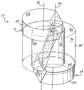
Referring to FIG. _, the interconnect contact device 10,
which is shown as being used in grounding application,
includes, in its most general sense, cooperatively interfacing
first 12 and second 14 contact elements, and an elastomeric
member 16 resiliently retaining the first contact element 12
in engagement against the second contact element 14 and
biasing the first element 12 relative to the second element 14
to a desired relative disposition so as to accomplish a wiping
action at a cooperative interface therebetween. It may be
fairly said that the cooperating first 12 and second 14
contact elements of the device 10, as shown in the "passive"
condition or state of F=G. 1, somewhat resemble an obliquely
bisected (i.e., from the bottom left to top right as shown in
FIG. 1) aligned spool or cum~bell whose halves laterally shift
(i.e., the ends thereof move out of axial alignment).
Preferably, but not necessarily, the contact elements 12 and
14 are structured equivalently, with the device 10 being '
-10-
' ; .~C',~~1 l:L'..:i~~LY~.a... .v pouw "t'. ~ Mr... . , v' a. ...~:
.. . _ . .. . .. _. . .. .. ....., . ...J : , .'... . . ~ . . ..r , . -.
.CA 02321623'2000-10-02~
configured such that one contact element is "inverted"
relative to the other, one substantially but not necessarily
directly atop and in substantial alignment with the other
contact element. This configuration, generally the engagement
of the contact elements for responsive displacement of one
with respect to the oter, is resiliently maintained by the
elastomeric member positioned about the interfacing contact
elements.
Each of the contact elements 12 and 14 generally has a
negative of surface nor:;:al axis (i.e., first axis 18 for the
first contact element ;2 and second axis 20 for the second
contact element 14) and includes joined body 22 and base ~4
components that can be cylindrical in shape, as shown, the
base 24 being of larger diameter than the body 22 and aligned
IS therewith. The bodies 22 of the contact elements 12 and 14
engage each other to thereby generally form a cooperative
interface therebetween, while the bases 24 thereof engage and
indirectly conductively join, via the cooperative interface,
the contacts to a device for test and a test board. In all
cases, the base 24, 25 of each contact element 12 and 14
preferably extends farther from its axis 18 or 20 than the
body compcnent 22 , and is preferably integral with the body
ccmponent 22.
-11-
_ . . ...~.3~;.~~. . .. ..w;....i;,.,~.. ..._.. . ,...._...... . ... . .. .-
tv!.w ., w. Jvl. . , ;.
. . _ . . .. _ _ ._. . _., .._ _ .. _ ..,. . ,.......... ........ >..-,~~:
..._
CA 02321623 2000-10-02
In addition to body 22 and base 24 components, each
contact element 12 and 14 has a face (typically planar) or
surface 26 obliquely extending, relative to the element's axis
18 or 20, across its body 22. Extension of surface 26
preferably continues across the base component 24 of the
contact element 12 or .4. In as much as the bodies 22 of the
contact elements 12 and 14 are in engagement, it is the
engagement of the partial ly aligning planar faces 26 that form
or define the cooperat_Ve interface between the first 12 and
second 14 contact eleme_-.ts .
The elastomeric member 16 can be generally band like (as
illustrated) , and can be tubular in character, having an inner
surface 28, engaging the contact elements 12 and 14, and an
outer surface 30 adjacent the test apparatus. The objective of
IS the resilient member is to maintain the orientation of the
cooperatively interfacing first and second contact elements
and bias elements 12 and 14 to their "passive" condition. The
member 16, which is gene=ally an elastomeric material such as
silicon rubber cr polyethylene, is positioned about the
contact element bodies 22 for compression thereof. Responsive
displacement of one relative to the other can thereby be
permitted, and the many benefits accruing therefrom (Gs
discussed with respect to FIGS. 3 & 4) can be achieved.
-12-
.. .... . .. _.. ' . .3~'.u.~.l::ujl'.. ...L.~.~AiF..'...,...:.,~
..:r5stl~~.~.' "~LW'<a:~;E4:3w'.~,:.,'rw'.:~'. ~ ..~ ,.w.. . .,~..
.'t.~...wy7.', ,.
..-._. .. ~ ... ,.~_ r... ~ - ..4... . -.... ., ...r .-. , ... " :, w.m. '
CA 02321623 2000-10-02
Preferably, the elastomeric member 16 is dimensioned such that
its outer surface 30 is substantially flush with the base
"facing" 25 (i.e., the maximum dimension of the elastomeric
member 16 is about equal to the maximum dimension of the base
S components 24 of each ef the contact elements 12 and 14).
The dimensions of ~he contact device, particularly the
base diameters of the contact element engagement areas, are
predicated upon the package and its pad size. However, each
of the base components of the contact elements provides an
appreciable contact area for the IC and PC board, particularly
when compared to pogo-pins, etc.
The contact elements are preferably fabricated from a
beryllium/copper (Be/Cu) composite, although other known
conducting materials are likewise contemplated and embraced.
IS The elastomeric member is illustrated as being generally
cylindrical or tube-shaped. Such a shape is not, however,
required.
Referring to FIG. 2, the contact device 10 is shown as
part of a test assembly 40, which orients the invention with
respect to the surface to which the test assembly is mounted.
The assembly 40 also orients the contacts 12 and 14 relative
to the IC device which is to be inserted into the assembly for
testing purposes. Generally, the test assembly 40 includes an f
-13-
..::. . .~ . - ; -'k~,ieu... ' . . . . ,
.-- - . - . CA 02321623 2000-.10-Oi~... . ._, . . . .. . .__., , . . .. . . ..
.. .. ..
alignment plate 42 having a socket 44 for receiving an IC
intended for testing, an underlaying housing or layer 46
overlying a PC board (not shown) , and the contact device 10
positioned for conductively joining a device under test 48
within the socket 44 to the PC board. As shown, the device
under test 48 initially engages the first contact element 12
of the device 10.
Referring to FIGS . 3 & 4 , the interconnect contact device
is shown in cross section. Upon insertion, the I/0
10 components of the IC i~:pinge on the first (i.e., "upper")
contact element 12 of the device 10, and specifically the base
component 24 thereof. As the IC is pressed into the assembly,
denoted in FIG. 4 by the downward pointing upper arrowhead,
the first contact element 12 is forced to slide down and
IS across the planar face or surface 26 of the underlying
"stationary" second (i.e., "lower") contact element 14, which
is in conductive communication with the PC board (not shown).
Although the face 26 for each contact element 12 and 14
generally extends acrcss the body 22 thereof, it preferably
extends across both the body 22 and the base 24 components,
depending upon specific application objectives and
constraints. With such a configuration, there exists, during
back and forth sliding of the first contact element 12 upon
-14-
v..w. ~: ;, .~ y. ~.;_.. . _. .. ~ ~. ., ... ~ -,..y~ ,~ ._ . ~''~"'.u:.." -w.
.-.... y -:. ~_., o-.,.-_ :,. ' , .:..:.i ,..o.:.. n.., ~-. ~...
CA 02321623 2000-10-02
~,;~,
the second contact element 14, clearance for the first body
component 22 relative to the second contact element structure
14 to permit a maximum sliding travel distance for the first
contact element 12. As the first contact element 12 slides
across the second 14, z-axis compliance is provided, as well
as lateral translation in the plane of the lower surface of
the IC. The two dimensic::al sliding or "wiping" motion affords
two benefits: z-axis compliance protects the IC from damage
that might otherwise occur if the contact element or elements
were rigid, and the hcrizontal translation scrubs the I/O
component of the IC to clean them of debris and oxides that
might degrade electrical signal quality.
As is noted by comparison of FIGS. 3 & 4, during
engagement of the IC with the contact device (i.e., the
"active" state ef FIG. 4), the resilient member 16 is forced
to deform outwardly as the contact element "constrained"
within the elastomeric member radially expands. That is, in
going from a passive to an active condition, the negative ef
surface normal axes 18 and 20 of the contact elements 12 and
14 are driven Gpart to radially compress the elastomeric
member 16. Upon conclusion of testing and removal of the IC
from the socket 44 ( i . a . , a return to the passive state of
FIG. 3) , the elastomeric member 16 returns to its original
-15-
. ._ ~...:. _ .,. . ..y~,., . . .. .,. -w..~ , . . . . .. ,_.. .. . . . . . .'
.. _. . .. . ... ., :. . . .: .......:.... .~ _. . i.'..~ ~ .. ._. ...- .-- .
..
CA 02321623 2000-10-02
state and thereby permits return of the f first 12 and second 14
contact elements to their passive, at-rest positions.
It will be understood that, in addition to the previously
noted functions of maintaining the positioning of the contact
elements and providing upward and compressive radial forces to
the elements, the elastomeric member further shields the
sliding surfaces of the contact elements from debris . This
enables a high degree c. isolation of the device to thereby
minimize cross talk.
It will be understood that this disclosure, in many
respects, is only ills=trative. Changes may be made in
details, particularly fir. r.-~atters of shape, size, material, and
arrangement of parts without exceeding the scope of the
invention. Accordingly, the scope of the invention is as
defined in the language of the Gppended claims.
-16-