Note: Descriptions are shown in the official language in which they were submitted.
. CA 02321624 2000-08-29
- ' WO 99/56339 PCT/US99109337
1 MICROWAVE CHANNELIZED BANDPASS FILTER HAVING TWO CHANNELS
2
3 BACKGROUND OF THE INVENTION
4
1. Field of the Invention
6 The invention relates to microwave filters that are
7 compatible with micrav~iave monolithic integrated circuit (MMIC)
8 technology, and more particular to a microwave channelized
9 bandpass filter having two channels.
11 2. Description of Background Art
12 There is an urgent need for small, light-weight, low-cost
13 microwave filters that are compatible with microwave monolithic
34 integrated circuit (MMIC? technology, yet offer low insertion
Loss and high selectivity. Such filters are needed particularly
16 for next-generation ultra-compact multi-function systems for
17 defense applications. There is also a need for such filters in
18 frequency synthesizers and in commercial mobile communication
19 systems.
The concept of the microwave channelized filter, as
21 described in the present inventor's U.S. Patent 5,339,057 and in
22 C. Rauscher, "Microwave Channelized Active Filters ...," IEEE
23 Transactions on Microwave Theory and Techniques, pp. 122-123,
24 Jan. 1996, both expressly incorporated by reference, marked a
WO 99/56339 CA 0 2 3 216 2 4 2 0 0 0 - 0 s - 2 9 PCT/US99/09337
~ Y
1 major breakthrough with regard to the realization of miniature,
2 highly selective microwave filters. The breakthrough is based on
3 an active-filter concept that uses parallel-connected, frequency-
4 selective network branches to accomplish filter selectivity
through constructive and destructive interference among branch
6 signal components, thereby circumventing limitations related to
7 circuit stability and noise that have rendered earlier microwave
8 active-filter approaches impractical. The feed-forward
9 architectures of these filters resemble those of analog
l0 transversal filters, and exhibit performance and operational
11 advantages similar to those of transversal filters. However, the
12 channelized filters use frequency-selective feed-forward signal
13 paths (instead of the frequency-independent ones used in
14 transversal solutions) which, in turn, reduces the required
number of signal paths or branches to two or three, down from the
16 fifty to one hundred branches needed in the case of analog
17 transversal filters. The space savings are dramatic, without
18 compromise of performance.
19 Channelized filters with low-pass, high-pass, and band-
reject responses all require a minimum of two feed-forward
21 branches. On the other hand, channelized filters with bandpass
22 responses, which encompass the majority of applications, have to
23 date required a minimum of three branches. Adding the third
24 branch causes the actual filter size to increase by far more than
2
t
W099/56339 CA 02321624 2000-os-29
y
PCT/US99/09337
1 the simple three-to-two ratio which is suggested by the
2 respective numbers of branches in the two types of circuits.
3 This is due to the relatively large circuit area needed to
4 realize three-way signal splitters and combiners, when compared
to the much smaller and simpler two-way splitters and combiners
6 used in low-pass, high-pass, and band-reject situations.
7
8 SUNff~IARY OF THE INVENTION
9 Accordingly, there is a need for a reduction in the circuit
area occupied by a channelized filter with a bandpass response.
11 To address this need, the invention provides a channelized
12 bandpass filter with only two branches which provide respective
13 frequency-selective signal paths that may contain substantially
14 unilateral circuits in either or both branches to help estsblish
feed-forward signal flow.
16 In this connection, the invention represents a significant
17 improvement over the known channelized filters. Limiting the
18 number of frequency-selective feed-forward branches to two has
19 not previously been thought possible in a bandpass filter. It
allows a channelized bandpass filter to be realized in a fraction
21 of the space formerly needed to implement a bandpass filter in
22 accordance with the original channelized filter concept.
23 According to another aspect of the invention, the two
24 branches may be provided with bandpass transfer characteristics
3
. . WO 99/56339 CA 0 2 3 216 2 4 2 0 0 0 - 0 s - 2 9 PCT/US99/09337
t
1 of different orders and shapes. One branch may be provided with
2 a second-order response and the other branch may be provided with
3 a fourth-order response, for example. In contrast, the known
4 channelized bandpass filters had three branches with simpler
S transfer characteristics of the same order.
6 According to a further aspect of the invention, two-way
7 signal splitting and combining to define the two channels may be
8 performed with in-phase splitters and combiners, for example.
9 Alternatively, two-way splitting and combining can be performed
with diplexer circuits, each composed of two bandpass filters.
11 Combinations of the two types of splitting and combining are also
12 possible. In both of these splitting and combining arrangements,
13 the two respective passband responses intentionally occupy, at
14 least in part, a common frequency range within the composite
filter passband. That is, despite the generally different
16 respective shapes, bandwidths and/or orders that the two branch
17 filter responses may exhibit, their passband center frequencies
18 at least approximately coincide. Separate branch filters having
19 responses with overlapping passbands have not previously been
used in a channelized bandpass filter. This is particularly
21 remarkable in the case of the diplexer-coupled arrangement.
22 Conventionally, diplexers have been constructed to have a pair of
23 distinct, separated frequency response bands, not overlapping
24 response passbands as in this aspect of the present invention. '
4
' . WO 99/56339 ca o 2 3 216 2 4 2 0 0 0 - o s - 2 9 p~~S99/09337
.-
The sharing of passband frequencies and the approximately
2 common center frequencies of the respective branches represent an
3 important improvement according to the invention. In en~,ra~r
4 the three branch filter responses in the prior-art three-channel
filter configuration must inevitably have different center
6 frequencies in order for the three-channel filter to function as
7 intended.
8 Thus, the disclosed microwave channelized bandpass filter
9 results in a dramatic reduction in the size of previous bandpass
ZO ffilters. When compared to earlier three-branch configurations,
11 the reduction in size originates from the ability to make do with
12 only two branches, albeit branches of a somewhat higher level of
13 circuit sophistication.
14 If one or more of the substantially unilateral circuits used
1~ to help establish feed-forward branch signal flow are
16 amplifiers, the two-branch approach can be rendered very tolerant
17 of passive-circuit losses, allowing overall circuit size to be
18 kept to a minimum through reliance on lumped passive circuit
19 elements, which tend to be rather lossy. This, in turn, makes it
20 possible to realize high-selectivity, low-noise, stable filters
21 in MMIC form.
22 The disclosed circuit can be implemented either in hybrid-
5
WO 99/56339 CA 0 2 3 216 2 4 2 0 0 0 - 0 s - 2 9 PCT/US99109337
r
1 circuit format, or in MMIC form, for example. In addition, any
2 other combination or selection of substantially unilateral two-
3 port components and/or and passive, frequency-selective branch
4 circuits can be used to implement the invention. Aside from
amplifiers which are typically used, optional unilateral
6 components may include, for example, nonrecipocal ferrite
7 devices, such as circulators and isolators. The implementation
8 may also involve, for instance, the use of high-Q dielectric
9 resonators to provide ultra-sharp filter characteristics in
situations where performance is important. In such a situation
11 it may be less important to realize the circuit as a planar
12 structure. Even though channelized filters can be rendered very
13 tolerant of passive circuit losses, the lower these losses are,
14 the better. Planar structures are thought to be generally
preferable from a fabrication and size point of view, other
16 factors being equal.
17 Other features and advantages of the invention will be
18 understood from the following detailed description of embodiments
19 thereof, with reference to the drawings.
21 BRIEF DESCRIPTION OF THE DRAWINGS
22 fiig. 1 is a circuit diagram showing a first embodiment of
23 the invention, having feed-forward branches defined between a
24 pair of signal splatters;
6
t
WO 99/56339 CA 0 2 3 216 2 4 2 0 0 0 - 0 s - 2 9 pCT~S99/09337
Fig. 2 is a circuit diagram showing a second embodiment of
2 the invention, having feed-forward branches defined between a
pair of diplexers;
Fig. 3 is a graph showing the respective transfer
characteristics of the feed-forward branches in the circuit shown
6 in Fig. 1;
7 Fig. 4 is a graph showing the composite transfer
8 characteristics of the circuit shown in Fig. 1;
Fig. 5 is a circuit diagram showing a third embodiment of
the invention which is similar to the first embodiment, having in
11 addition delay lines in the respective feed-forward branches; and
12 Fig. 6 is a circuit diagram showing a fourth embodiment of
13 the invention which is similar to the second embodiment, having
14 in addition delay lines in the respective feed-forward branches.
16 DETAILED DESCRIPTION OF EMBODIMENTS OF THE INVENTION
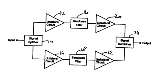
1~ A first embodiment of the invention is shown in Fig. 1. An
18 input signal is split by a signal splitter 10 to produce two
19 signals of same or different strengths which are then passed on
to respective unilateral circuits 12 and 14, either or both of
21 which.are optional: The two signals are applied to first and
22 second'~bandpass filters 16 and 18 having different
23 characteristics. In this example, the_first bandpass filter has
24 a second-order response and the second bandpass filter has a
7
WO 99/56339 CA 0 2 3 216 2 4 2 0 0 0 - 0 8 - 2 9 PC'TIUS99/09337
F
1 fourth-order response. The respective outputs of the bandpass
2 filters 16 and 18 are passed through corresponding optional
3 unilateral circuits 20 and 22, and then combined by a combiner 24
4 to produce an output signal.
S In a second embodiment of the invention, shown in Fig. 2, a
6 first diplexer 30 comprises first and second bandpass filters 32
7 and 34 having different characteristics. The respective diplexer
8 outputs of the first and second bandpass filters 32 and 34 are
9 passed on to corresponding unilateral branch circuits 36 and 38,
one of which may be optional. The outputs of the unilateral
11 circuits 36 and 38 are then applied as respective inputs to a
12 second diplexer 40, which comprises third and fourth bandpass
13 filters 42 and 44 having different characteristics which
14 correspond to the characteristics of the bandpass filters 32 and
34. In this example, as in the first embodiment of the
16 invention, the combination of the first and third bandpass
17 filters 32,42 provides a lower-order response than the
18 combination of the second and fourth bandpass filters 34,44. To
19 accomplish this, it is often preferable but not mandatory for the
first and third bandpass filters 32, 42 to have similar lower-
21 order responses, and for the second and fourth bandpass filters
22 34, 44. to have similar higher-order responses.
23 At the desired transmission-null frequency below the
24 passband, the two branch amplitude responses should substantially
8
WO 99/56339 CA 0 2 3 216 2 4 2 0 0 0 - 0 s - 2 9 pCT~S99/09337
1 coincide and their respective phases should be at least
2 approximately 180 degrees apart, thus permitting complete or
3 partial cancellation between the two branch signals at the output
4 of the composite channelized filter.
In the desired passband region, the respective amplitude and
6 phase responses of the two branches should permit the respective
7 branch responses to form a flat overall passband response. Thus,
8 the two branch signals should constructively interact across the
9 passband frequencies, and the branch amplitude characteristics
should be chosen so as to complement each other when added at the
11 composite filter output.
12 At the desired transmission null frequency above the
13 passband, the two branch signals should again substantially
14 coincide in amplitude, and should again be at least approximately
180 degrees out of phase to permit complete or partial
16 cancellation.
The first and second embodiments achieve these results most
18 compactly, with filters of different respective orders and
19 response shapes in the two branches. The lower-order branch will
exhibit more gradually sloping filter skirts than its higher-
21 order counterpart, thus permitting an amplitude response
22 crossover between the respective branch signal responses. At the
23 same time, the different filter orders associated with the two
24 branches provide the necessary phase differential between the
9
WO 99/56339 CA 0 2 3 216 2 4 2 0 0 0 - 0 s - 2 9 PCT/US99/09337
1 branch signals, going from approximately 180 degrees out of phase .
2 at the low-end null frequency, to in-phase in the vicinity of the
3 passband center, to again approximately 180 degrees out of phase
4 at the desired high-end null frequency.
Thus, the first and second embodiments are believed to be
6 the most advantageous way of implementing the invention, because
7 resonant structures forming branch filters provide the most
8 compact structure for realizing fast-changing phase responses, as
9 are needed to spin the branch phase differential through a total
of 360 degrees over the preferably narrow frequency band between
I1 desired transmission nulls.
12 Summarizing, in the foregoing embodiments, both the orders
13 and the shapes of the respective branch amplitude responses will
14 differ. In particular, the bandwidths of the two branch
responses may differ. However, they preferably have
16 approximately the same center frequency, with some offset
17 allowed, as long as the composite filter exhibits acceptably
18 sharp amplitude roll-off above and below the passband, as
19 determined by the positions of the transmission nulls. As
previously discussed, the cancellation of the two branch signals
21 at the designated transmission null frequencies need not be
22 complete according to the invention, as it can be advantagous,
23 depending on the application, to trade null signal rejection
24 against other response attributes.
WO 99/56339 CA 0 2 3 216 2 4 2 0 0 0 - O s - 2 9 p~NS99/09337
1 An experimental bandpass filter was constructed as shown in
2 Fig. 1, employing N~iIC amplifiers as unilateral branch circuits.
3 The filter's two-channel transfer characteristics are depicted in
4 Fig. 3, in which the dotted lines 52, 56 indicate calculated
results, and the solid lines 50, 54 depict measured responses.
6 The marked differences between the respective responses of the
? two channels should be-noted. The response 50 of the first
8 bandpass filter 16 is a second-order response and the response 54
9 of the second bandpass filter 18 is a fourth-order response. The
respective responses add up in the passband to provide a well
11 behaved passband response, and are 180 degrees out of phase at
12 their two outward cross-over points 58 and 60 to introduce zeros
13 of transmission through cancellation. The resulting measured
14 response ?0 and predicted response ?2 of the composite
channelized active filter are shown in Fig. 4.
16 In some situations it may be difficult for the branch
1? filters of the first and second embodiments to achieve the
18 desired fast phase rotations between the upper and lower null
19 frequencies. To address this problem, according to third and
fourth embodiments of the invention, the composite filter may be
21 constructed as shown in Figs. 5 and 6, which correspond
22 respectively to Figs. 1 and 2, Like elements and parts being
23 indicated by identical reference numerals.
24 In the circuit of Fig. 5, in addition to the elements in the
11
_ . WO 99/56339 CA 0 2 3 216 2 4 2 0 0 0 - 0 s - 2 9 PCT/US99/09337
1 circuit of Fig. 1, a delay line 17 is connected between the
2 bandpass filter 16 and the unilateral branch circuit 20, and
3 likewise, a delay line 19 is connected between the bandpass
4 filter 18 and the unilateral branch circuit 22. As in the first
embodiment, the incorporation of unilateral circuits into
6 respective branches is optional as long as feed-forward branch
7 signal flow is established through alternate means, such as the
8 design of the signal splitter 10 and/or signal combiner 24 shown
9 in Fig. 5.
In the circuit of Fig. 6, in addition to the elements in the
11 circuit of Fig. 2, a delay line 37 is connected between the
12 optional unilateral circuit 36 and the bandpass filter 42, and
13 likewise, a delay line 39 is connected between the optional
14 unilateral circuit 38 and the bandpass filter 44. In this
configuration, at least one branch will contain at least one
16 unilateral circuit to establish substantially feed-forward branch
17 signal flow.
18 Either of the delay lines may be omitted, or placed at a
19 different location in the circuit, as long as the desired
composite response is obtained. The delay lines may be provided
21 by transmission line segments, for example.
22 In the third and fourth embodiments, bandpass filters having
23 similar behavior and the same filter order may be used, in which
24 case the needed fast phase rotations between the branch signals
12
t
W099/56339 CA 02321624 2000-os-29
- - PCT/US99/09337
1 may be achieved by the delay lines. The drawback of this scheme,
2 however, is that in a filter with a narrow passband, where the
3 phase differential between the branches may have to swing through
4 360 degrees over a narrow frequency range (from one null or
approximation thereof to the other), a very long time delay
6 differential between the branches may be required to achieve
7 sufficiently fast phase rotations. The resultant large combined
8 delay Line length in turn increases the physical dimensions of
9 the filter, which is not desirable.
Thus, to obtain faster phase rotations without increasing
11 the physical dimensions of the filter, a combination of the
12 mentioned approaches can be used. In other words, the necessary
13 phase rotation and the shaping of the amplitude response are
14 accomplished predominantly through the use of branch filters with
IS different orders and shapes, as described above in connectica
16 with the first and second embodiments, and delay lines such as
17 short transmission line segments are used to obtain fine phase
18 adjustment in one or both of the two branches.
19 Although embodiments of the invention have been descrired
herein, the invention is not limited to such embodiments, bLt
21 rather includes any modifications, variations and equivalent
22 which may occur to those having the ordinary level of skill in
23 the art. This pertains, in particular, to the ways in which
24 branch feed-forward signal flow is substantially achieved ar_3
13
WO 99/56339 CA 0 2 3 216 2 4 2 0 0 0 - 0 s - 2 9 PCT/US99/09337
' a
1 branch frequency selectivity is implemented.
2
14
1