Note: Descriptions are shown in the official language in which they were submitted.
CA 02321744 2000-08-29
METHOD OF FABRICATING OPTICAL NONLINEAR THIN FILM WAVEGUIDE AND
OPTICAL NONLINEAR THIN FILM WAVEGUIDE
TECHNICAL FIELD
The present invention relates to a method of fabricating
an optically nonlinear thin film waveguide using a glass substrate,
and to an optically nonlinear thin film waveguide. More
particularly, the present invention relates to controlling the
shape of a waveguide having optical nonlinearity.
Optical functional elements utilizing second-order optical
nonlinearity are known. While such elements are usually formed
of a crystalline material, optical fibers are formed of a glass
material. Considering cost and compatibility with an optical
fiber, a need exists for fabricating the optical functional
element of a glass material. In addition, as a planar element
is suitable for achieving various optical control (signal
control) functions, an optical functional element formed of a
glass substrate is desired.
A method of fabricating a planar optical waveguide of a
glass material is disclosed in Japanese Patent Laid-Open
Publication No. Hei 8-146475. According to the method disclosed
in that document, a glass film dispersed with fine particles is
deposited on a glass substrate, and a resist mask is formed of
photoresist over a portion to serve as a core. Next, the portion
of the particle dispersed glass film that is not covered by the
resist mask is removed by reactive ion etching to form an optical
1
CA 02321744 2000-08-29
waveguide (core) portion. After removing the resist mask, a glass
film is deposited to surround the core, and this portion serves
as cladding. High power laser light is irradiated to a part of
the core portion of the thus formed optical waveguide, thereby
imparting high optical nonlinearity to the irradiated part.
Although the above-described method of fabricating a planar
optical wave guide requires an etching step for leaving the portion
of the resist film corresponding to the core portion, etching the
film to leave only the core is difficult because this portion is
thin. Also, optical nonlinearity obtained by this method is
third-order nonlinearity, not second-order nonlinearity.
Consequently, only a small nonlinearity is obtained, and
therefore it is difficult to implement an element which
sufficiently operates as an optical element.
RELATED ART
The applicant proposed a method of manufacturing a planar
optical waveguide by UV-excited poling in Japanese Patent
Application No. Hei 8-244965. According to this method, a pair
of electrodes are formed on the surface of a glass substrate.
Using the electrodes as a mask, a gap portion between the
electrodes on the surface of the glass substrate is doped with
germanium ( Ge ) , so that the portion serves as a core . By applying
a high voltage across the gap between the electrodes while
irradiating ultraviolet rays, the core is subjected to
ultraviolet poling and given second-order optical nonlinearity.
The optical nonlinearity induced by UV poling is substantially
2
CA 02321744 2000-08-29
as high as that of a crystalline material, such as LiNbO,, and
therefore the planar waveguide thus obtained can be used for
forming a wide variety of functional optical waveguides.
It should be noted that single optical mode propagation and
operation are essential to functional optical waveguides, such
as optical switches and optical modulators used for optical
communication, optical measurement, optical information
processing, or the like. When a plurality of optical modes are
present, propagation constants of the respective modes
(refractive indices for the respective modes) are different, and
therefore operation voltages for switching or the like utilizing
optical interference effect will be different. Thus, in order
for an optical waveguide to achieve operation such as switching,
the waveguide is required to have a shape that allows single mode
optical propagation.
The shape of an optical waveguide is determined by a
combination of its refractive index and three dimensional size .
According to the applicant's method outlined above, the thickness
of an optical waveguide ( depth from the surface of the substrate )
formed by W-excited poling is controlled using optical
absorption of the substrate to change the intensity of ultraviolet
radiation.
In order to achieve a single mode, the optical waveguide
must have the smallest possible size, and the light intensity of
ultraviolet radiation must be decreased for this purpose.
However, the shape of the waveguide and the induced optical
nonlinearity cannot be controlled independently from each other
3
CA 02321744 2000-08-29
because the induced optical nonlinearity is also dependent on the
light intensity of ultraviolet radiation. Further, higher
optical nonlinearity is obtained as the intensity of ultraviolet
radiation increases. Consequently, the size of the waveguide is
increased for the sake of imparting a high optical nonlinearity,
making it impossible to achieve single mode propagation.
DISCLOSURE OF THE INVENTION
The present invention aims to provide an optically
nonlinear waveguide and a method of fabricating the optically
nonlinear thin film waveguide wherein the optically nonlinear
waveguide formed of a glass material has a sufficiently high
second-order optical nonlinearity, and allows a proper three-
dimensional shape to be obtained.
The fabricating method according to the present invention
comprises the steps of forming a thin SiOz film containing Ge on
a glass substrate, forming thin metal electrode films on the thin
Si02 film with a gap between the electrode films having a shape
corresponding to a waveguide pattern, and irradiating the Ge-
containing thin Si02 film with ultraviolet radiation through the
gap while applying a voltage across the gap between the thin metal
electrode films.
Thus, the thin Si02 film containing Ge is formed on the glass
substrate, and, therefore, it is limited to the Ge-containing thin
Si0= film where second-order optical nonlinearity is induced by
UV-excited poling . As a result , the width can be defined by the
shape of the electrodes, and the depth can be controlled by the
4
CA 02321744 2000-08-29
thickness of the Ge-containing thin Si02 film, so that the shape
of the optically nonlinear waveguide can be controlled in three
dimensions. A single mode propagation can be achieved in the
optically nonlinear waveguide, to thereby ensure operation, such
as switching, in the optically nonlinear waveguide. While the
glass substrate is preferably formed of SiOz glass, other
materials, such as sodium glass, can also be employed.
The method of fabricating an optically nonlinear thin film
waveguide according to the present invention may further comprise
the steps of providing a thin transparent insulating film on the
thin metal electrode films to cover at least said gap portion,
and irradiating the Ge-containing thin Si02 film with ultraviolet
radiation through the gap between thin metal electrode films while
applying a voltage across said gap. Such provision of the
insulating film can prevent electric discharge which would
otherwise be caused by dielectric breakdown during application
of a voltage across the gap between the metal electrodes for
UV-excited poling. The thin insulating film must be formed of
a material having a high breakdown voltage and transmitting
ultraviolet radiation, preferably Si02.
Preferably, the optically nonlinear thin film waveguide is
formed in a vacuum chamber. Because dielectric breakdown does
not occur in a vacuum as it does in air, a sufficiently high voltage
can be applied across the electrodes for W-poling.
An optically nonlinear thin film waveguide according to the
present invention includes a thin SiOz film containing Ge and
formed on a glass substrate, and thin metal electrode films formed
5
CA 02321744 2000-08-29
on the Ge-containing thin Si02 film with a gap between the
electrode films having a shape corresponding to a waveguide
pattern, wherein the portion of the Ge-containing thin silica film
corresponding to the gap between the thin metal electrode films
exhibits second-order optical nonlinearity.
The optically nonlinear thin film waveguide according to
the present invention may further include a thin transparent
insulating film formed on the thin metal electrode films to cover
the gap.
BRIEF DESCRIPTION OF THE DRAWINGS
Fig. 1 illustrates a configuration of an optically
nonlinear thin film wave guide according to one embodiment of the
present invention.
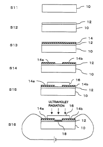
Fig. 2 illustrates steps of fabricating the optically
nonlinear thin film waveguide.
Fig. 3 illustrates another exemplary configuration of the
optically nonlinear thin film waveguide.
Fig. 4 illustrates fabrication of the optically nonlinear
thin film waveguide in a vacuum chamber.
BEST MODE FOR CARRYING OUT THE INVENTION
A preferred embodiment of the present invention will next
be described with reference to the drawings.
[Configuration of Optically Nonlinear Thin Film Waveguide]
Fig. 1 schematically shows a configuration of an optically
nonlinear thin film waveguide ( planar waveguide ) according to the
6
CA 02321744 2000-08-29
present invention. A glass substrate 10 is formed of silica glass
(Si02 glass) as a flat sheet. On a surface of this substrate,
a Ge-doped thin SiOz film 12 is formed, i.e. a thin Si02 film
containing Ge, having a thickness of approximately 1-5 ,~ m and
a Ge concentration of approximately 1-30 mold . The specific
values are determined in accordance with the specification of the
planar waveguide, such as the wavelength to be used. Electrodes
14a and 14b are formed on the Ge-doped SiOz film 12, patterned
to a prescribed shape and facing each other with a prescribed gap
therebetween. The electrodes 14a and 14b are formed of thin films
of, for example, aluminum (Al). A thin transparent insulating
film 16 is formed covering the electrodes 14a and 14b and the gap
therebetween.~ In this particular example, the thin insulating
film 16 is formed of SiOz .
A channel portion 18 is formed at a portion of the Ge-doped
SiOz film 12 corresponding to the gap between the electrodes 14a
and 14b, and to this channel portion 18 optical nonlinearity is
imparted by UV-excited poling. As a result, optical
characteristics of the channel portion 18 can be controlled by
a voltage applied across the electrodes 14a and 14b. Light
propagating through the channel portion 18 is controlled by the
voltage applied across the electrodes 14a and 14b, whereby a
planar waveguide functions as an optical functional element.
While SiOZ glass is used for the glass substrate 10 in the
above-described example, other materials, such as sodium glass,
can also be employed.
[Fabricating Method]
7
CA 02321744 2000-08-29
A method of fabricating the above-described planar
waveguide will be described with reference to Fig. 2. First, the
glass substrate 10 formed of a planar SiOz glass sheet is prepared
(S11), and then introduced into a vacuum chamber to form the
Ge-doped SiOz film 12 on the surface of the substrate 10 (S12).
The Ge-doped SiOz film 12 is formed by, for example, electron beam
evaporation method using a sintered material containing 20% of
Ge02 as an evaporation source. While to obtain a dense film an
assist method using an Ar' beam as an assist beam is preferable,
other film formation methods may also be employed.
A metal film 14 is formed over the Ge-doped SiOZ film 12
( S13 ) . Although A1 is used in this example, other metals may also
be employed, and the metal film 14 may be formed by other methods
than the evaporation method.
Next, a prescribed portion of the metal film 14 is removed
by etching to form the pair of electrodes 14a and 14b ( S14 ) . In
this particular example, a linear gap is formed between these
electrodes 14a and 14b. Etching is performed by photolithography
or the like. More specifically, resist is deposited over the
entire surface of the metal film 14, and light is irradiated
through a mask pattern used for forming the gap, thereby exposing
a prescribed portion of the resist to the light. The portion
corresponding to the gap is removed as a result of the light
irradiation, thereby exposing the corresponding portion of the
metal film 14, and the exposed portion of the metal film 14 is
removed. Finally, the resist is removed to form the electrodes
14a and 14b facing each other with a gap therebetween.
8
CA 02321744 2000-08-29
A thin insulating film 16 is formed on the electrodes 14a
and 14b (S15). This thin film 16 is formed of SiOz by an electron
beam evaporation method or the like using SiOZ as an evaporation
source . The film 16 may be formed over the entire surf ace or over
part of the surface, but is required to cover at least the gap
portion formed by the electrodes 14a and 14b. In addition, the
film 16 may be formed of any material, such as Mg0 or MgFz, as
long as the material can transmit ultraviolet radiation and has
a high breakdown voltage.
Thus, after the gap between the electrodes 14a and 14b is
covered with the insulating film 16, ultraviolet light is
irradiated while applying a prescribed high voltage across the
electrodes 14a and 14b, thereby performing UV-excited poling of
the portion of the Ge-doped SiOz film 12 located between the
electrodes 14a and 14b to form a channel portion 18 (S16).
More specifically, a voltage of approximately 1kV is
applied across the electrodes 14a and 14b, thereby applying an
electric field of approximately 106 V/cm to the channel portion
18. Under such circumstances, the channel portion 18 is
irradiated with ultraviolet radiation using a pulsed ArF excimer
laser (193 nm wavelength). A laser having an energy density of
approximately 36 mJ/cmZ and a pulse repetition rate of
approximately 10 pps (pulse/second) is used to irradiate the
channel portion 18 for a period of approximately 10-30 minutes.
When such a high voltage is applied across the electrodes
14a and 14b, electric discharge may occur at the portion facing
the gap. According to the present embodiment, however, this
9
CA 02321744 2000-08-29
portion is covered with, the insulating film 16 , thereby preventing
electric discharge which would otherwise occur at the gap between
the electrodes 14a and 14b due to air breakdown, and achieving
effective UV-excited poling. It should be noted that as the
electric field causing air breakdown is approximately 10° V/cm,
applying a voltage of 106 V/cm to the channel portion 18 results
in electric discharge. Si02 is a preferable material for the
insulating film 16 because it transmits ultraviolet light ( at a
wavelength of, for example, 193 nm) and has a sufficiently high
breakdown voltage.
Thus , the channel portion 18 is given second-order optical
nonlinearity. In other words, the UV-excited poling process
described above provides the channel portion 18 with the
second-order optical nonlinearity withthe magnitude (d constant)
of 2 pm/V or more.
As described above, the Ge-doped Si02 film 12 is formed on
the glass substrate 10 in this embodiment, and therefore it is
limited to this film 12 where second-order optical nonlinearity
is induced by UV-excited poling. As a result, the width of the
waveguide can be defined by the shape of the electrodes 14a and
14b, and its depth can be controlled by the thickness of the
Ge-doped Si02 film 12 , so that the shape of the optically nonlinear
waveguide can be controlled in three dimensions. Consequently,
a single propagation mode can be achieved in the optically
nonlinear waveguide, ensuring operation, such as switching, at
the optically nonlinear waveguide.
While UV-excited poling is performed only at a single
CA 02321744 2000-08-29
portion in the above example , separate electrodes 14a and 14b may
preferably be formed at desired positions on the glass substrate
to form element regions with optical nonlinearity at the
respective positions on the glass substrate 10. It is also
5 preferable to restrict and define the position of the optical
waveguide by patterning the Ge-doped SiOz film 12 with
photolithography or the like. Further, it is also preferable,
as disclosed in Japanese Patent Application No. Hei 8-244965, to
alternately provide a region with optical nonlinearlity and an
10 ordinary region in a periodic manner to be used as a grating'
portion.
[Other Configurations]
The planar waveguide according to the present invention can
be used as various functional components. For example, as shown
in Fig. 3, the channel portion 18 may be formed as a coupler, in
which branched waveguides are converged once and then branched
again, and the electrodes 14a and 14b are preferably disposed at
the respective branched portions to which a voltage is applied.
The above-described configuration allows an optical phase
or the like to be controlled by adjusting the voltage applied to
the converged portion.
According to the optically nonlinear thin film waveguide
of the present invention, a portion with optical nonlinearity can
be formed at any desired position of the glass substrate 10, and,
therefore, various optical functional components and circuitscan
be formed as desired. For example, an optical switch/coupler,
a signal generator in a bi-directional optical transmission
11
CA 02321744 2000-08-29
system, and the like, can be formed by the optically nonlinear
waveguide of the present invention.
Further, the planar waveguide may be preferably fabricated
in a vacuum by UV-excited poling. Fig. 4 shows a configuration
of the device for such fabrication. A vacuum chamber 20 is formed
of crossing pipe channels with three closed ends and an end
connected to an exhaust system, such as a vacuum pump. A sample
mounting table 22 is provided in the pipe channel downwardly
extending in a vertical direction, and the glass substrate 10
having the electrodes 14a and 14b and the Ge-doped SiOz film 12
formed thereon is placed on the table 22. The electrodes 14a and
14b are connected to a power source outside the vacuum chamber.
The pipe channel upwardly extending in the vertical direction is
sealed by silica glass 24, through which ultraviolet radiation
is applied.
Using the above-described device, a high voltage is applied
to the electrodes 14a and 14b while irradiating the Ge-doped SiOz
film 12 with ultraviolet radiation. In contrast to air,
dielectric breakdown does not occur in a vacuum. Therefore, a
desired high voltage can be applied across the electrodes 14a and
14b to carry out UV-excited poling, to thereby impart desired
optical nonlinearity to the portion of the Ge-doped thin film 12
positioned between the electrodes . It should be noted that the
Ge-doped Si02 film 12, and the electrodes 14a and 14b are
preferably formed in the same vacuum chamber 20.
Using the above-described device, light was irradiated by
ArF excimer laser (193 nm wavelength) having an energy density
12
CA 02321744 2000-08-29
of 100 mJ/cmz for 104 pulses (lOpps). With the pressure in the
vacuum chamber 20 of approximately 10-6 Torr and the poling
electric field of 8 X 10° V/cm, optical nonlinearity of 3. 8~0. 3
pm/V was obtained at the channel region.
INDUSTRIAL APPLICABILITY
The optically nonlinear thin film waveguide of the present
invention can be used for an optical switch/coupler, a signal
generator in a bi-directional optical transmission system, and
the like.
13