Note: Descriptions are shown in the official language in which they were submitted.
CA 02321891 2000-08-23
t
V~rO 99/44042 PCT/GB99/00399
1
Waveguide Structures
This invention relates to waveguide structures, and particularly though not
exclusively to waveguide structures suitable for use as optical sensors.
Sensors which are capable of monitoring biological interactions in real time
and with high sensitivity are of considerable importance in life science
research.
Several sensors exist which monitor changes in the refractive index (or other
parameters) of a biological sample, caused by molecular interactions. In a
typical
sensor an evanescent wave associated with an optical mode existing in a high
refractive index dielectric layer of a waveguide extends into a biological
sample,
which is held in a gel. A change of the refractive index of the sample will
modify an
optical property of the waveguide mode, and detection of this change will
provide
dynamic information relating to interactions occurring within the biological
sample.
Known optical evanescent sensors include those based on surface plasmon
resonance and those based on dielectric waveguiding techniques (see for
example
Welford, K (1991) Surface plasmon-polaritons and their uses - Optical and
Quantum
Electronics, 23, 1-27; Smith, A.M. (1987) Optical waveguide immunosensors,
Proc.
SPIE 798 Fibre Optic Sensors Il, 206-213); R.H. Ritchie, Phys. Rev. 106, 874
(1957).
Sensors which use surface plasmon resonance comprise a thin metal layer
(typically a few tens or hundreds of Angstroms thick) deposited onto a
dielectric
prism or grating, and a sensing layer (or a fluid) whose optical properties
are of
interest provided at an opposite surface of the metal layer. Measurements are
made by
directing light via the prism or grating onto that side of the metal layer
which is not in
contact with the sensing layer, and detecting light which is reflected from
the same
side of the metal layer. A surface plasmon resonance excited by the incident
light will
result in the absorption of that incident light, and a consequent dip in the
reflected
light intensity. The condition for exciting a resonance (i.e. the angle of
incident light
which will excite a resonance) is sensitive to changes in the optical
properties of the
sensing layer. The optical properties of the sensing layer may be monitored by
detecting changes in the angle of incidence which excites a resonance
The resolution, and hence the sensitivity, of sensors which utilise surface
plasmon resonance is limited by the resonance width (i.e. the range of angles
of
CA 02321891 2000-08-23
VSO 99144042
7
PCT/GB99/00399
incident light which will excite resonance). This width is determined
ultimately by
the amount of absorption of incident light into the metal layer. Absorption is
,
considerable at wavelengths commonly used for biological measurements, and the
maximum resolution of surface plasmon sensors is correspondingly restricted.
The angle of incident light which excites a surface plasmon resonance will
alter if the wavelength of the incident light is changed. Variations in the
wavelength
of incident light will thus introduce an error into measurements. This is a
further
limitation of surface plasmon resonance sensors, since wavelength-stabilised
sources
of incident light are needed to allow accurate measurement.
A waveguide structure, based upon the surface plasmon resonance structure
and known as a leaky mode waveguide, is described by R.P. Podgorsek, H. Franke
and .T. Woods (1998) Monitoring of the Diffusion of Vapour Molecules in
Polymer
Films using SP-Leaky-Mode Spectroscopy, Sensors and Actuators B-Chemical,
Vo1.51, No.l-3, pp.l4b-151. The waveguide comprises a substrate, a thin metal
layer
disposed on top of the substrate, and a sensing layer whose optical properties
are of
interest disposed as a further layer on top of the layer of metal. The sensing
layer has
optical properties which change if the medium is exposed to conditions to be
sensed,
and may be for example dextran gel.
The leaky mode excited within the sensing layer is of a type known in the art
as a bulls mode. This contrasts with the mode which is excited by surface
plasmon
resonance sensors, which mode is known in the art as a surface mode. Generally
only
one mode may be excited in surface plasmon sensors (the mode must be a TM
mode),
whereas the leaky mode waveguide allows the excitation of a series of modes
(the
modes may be any combination of TE and TM).
A leaky mode of the waveguide, i.e. a bulk mode which is centred on the
sensing layer, is excited by directing light towards the layer of metal or
metal alloy '
through the substrate over a range of incident angles. The presence of an
excited ,
leaky mode is determined by detecting the intensity of light returned from the
waveguide over a range of angles. When light is coupled to a leaky ,mode of
the
waveguide this is seen as a dip in the intensity of light emitted from the
waveguide. A
change of an optical property of the sensing layer will modify the angle of
incident
CA 02321891 2000-08-23
w0 99/44042 PCT/GB99/00399
3
light required to excite the leaky mode. The angle at which the dip of
intensity is
returned from the waveguide will change accordingly.
The leaky mode waveguide is advantageous compared to surface plasmon
resonance because a bulk mode of the waveguide is excited rather than a
surface
mode. This bulk mode is centred on the sensing layer of the waveguide and is
therefore considerably more sensitive to changes of the optical properties of
the
sensing layer than the surface mode provided by surface plasmon resonance.
A disadvantage of known leaky mode waveguides is that detection optics are
required to detect a dip in the intensity of light returned from the
waveguide, and to
follow angular movement of that dip. The absence of light is inherently more
difficult
to detect than a peak of light intensity.
It is an object of the invention to provide a leaky mode waveguide which will
return a peak of intensity when a leaky waveguide mode is excited.
According to a first aspect of the invention there is provided an optical
sensor
comprising a waveguide having a substrate, a layer of metal or metal alloy
disposed
on top of the substrate, and a medium disposed as a sensing layer on top of
the layer
of metal or metal alloy, the medium having optical properties which change if
the
medium is exposed to conditions to be sensed, the sensor further comprising
means
for directing light towards the layer of metal or metal alloy through the
substrate over
a range of incident angles, and detection means for detecting the intensity of
light
returned from the waveguide over a range of detection angles, the means for
directing
light being configured to direct light such that a leaky waveguide mode is
excited
within the sensing layer, and the means for detecting the intensity of light
being
arranged to detect variations with detection angle in the intensity of
returned light
resulting from the excitation of the leaky waveguide mode; characterised in
that the
waveguide is configured such that the overlap of the optical field with the
layer of
metal or metal alloy is less for light incident at an angle which results in
excitation of
a leaky waveguide mode than for light incident at an angle which does not
result in
excitation of a leaky waveguide mode, whereby the detected intensity peaks~at
a
detection angle related to an incident angle which results in excitation of a
leaky
waveguide mode.
CA 02321891 2000-08-23
w0 99/44042
4
PCT/GB99/00399
The invention is advantageous because it allows for the easy detection of a
waveguide mode.
The term metal alloy is intended to include mixtures of metals and mixtures of
two or more elements which include at least one metal. Metals or metal alloys
are
used because they have a sufficiently high imaginary part of refractive index
that an
optical field extending into the metal or metal alloy suffers significant
loss. The term
metal or metal alloy is therefore intended to include any material having an
imaginary
part of refractive index comparable to that of a metal or metal alloy.
Preferably, the substrate comprises a prism or grating for coupling light into
the waveguide mode.
An optical source comprising a laser, a light emitting diode or a source
capable
of producing a broad spectrum of wavelengths of light may be used to provide
the
incident light. The use of a light emitting diode, or a broad band source, is
made
possible by the relative wavelength insensitivity of the waveguide mode of the
invention.
The detection means is preferably a charge-coupled-device array (CCD)
comprising cells of sufficiently small dimensions to allow resolution of the
intensity
variations resulting from the excitation of the waveguide mode.
The detection means may comprise a single photo-diode which is capable of
being translated across the light returned by the. waveguide. By translating
the photo-
diode through a series of positions, the photo-diode may be made to provide a
measurement of intensity at each position, thereby giving a measurement
similar to
that which will be provided by the CCD array.
The thickness of the layer of medium is preferably greater than 200nm, and
most preferably greater than 300nm. The layer of medium is required to be
thicker
than that typically used for surface plasmon resonance sensors, in order to
support the
waveguide mode which is excited within the medium.
According to a second aspect of the invention there is provided a method of
optical sensing comprising providing a waveguide comprising a substrate, a
layer of
metal or metal alloy disposed on top of the substrate, a medium disposed as a
sensing
layer on top of the layer of metal or metal alloy, the medium having optical
properties
which change if the medium is exposed to conditions to be sensed, directing
light
CA 02321891 2000-08-23
pCT/G 899/00399
WO 99/44042
towards the layer of metal or metal alloy through the substrate over a range
of incident
angles, and detecting the intensity of light returned from the waveguide over
a range
of angles, wherein the incident light is directed such that a waveguide mode
is excited
within the sensing layer, and variations in the intensity of returned light
resulting from
the excitation of the waveguide mode are detected; characterised in that the
waveguide is configured such that the overlap of the optical field with the
layer of
metal or metal alloy is less for light incident at an angle which results in
excitation of
a leaky waveguide mode than for light incident at an angle which does not
result in
excitation of a leaky waveguide mode, whereby the detected intensity peaks at
a
detection angle related to an incident angle which results in excitation of a
leaky
waveguide mode.
A disadvantage of conventional waveguides used for optical sensing is that
they do not provide an optical mode centred on a sensing layer. This problem
is
overcome by the leaky mode waveguide.
A limitation of the leaky mode waveguide is that leaky modes are sensitive to
changes of the dimensions of the layers comprising the waveguide. The
waveguide
must therefore be made with tight fabrication tolerances.
It is an object of the present invention to provide a waveguide structure
which
overcomes or mitigates the above disadvantage.
According to a third aspect of the invention there is provided a waveguide
structure comprising a medium disposed as a sensing layer, a second layer of
material
having a refractive index greater than that of the medium, and a substrate,
wherein the
structure defines a waveguide capable of supporting an optical mode confined
in the
sensing layer, the medium is adapted for performing chemical or biological
reactions
within the meditun which will result in a change of an optical property of the
sensing
layer of the waveguide, and the thickness and refractive indices of the layers
are
chosen such that an optical mode confined in the sensing layer will suffer
substantially anti-resonant reflection as a consequence of the interface
benveen the
sensing layer and the second layer and the interface between the second layer
and the
substrate.
The sensing layer is bounded on one side by a material whose refractive index
is lower than that of the sensing layer.
CA 02321891 2000-08-23
..
PCT/GB99/00399
WO 99144042
G
The reference in the statement of invention to a mode being confined in the
sensing layer of the waveguide structure is intended to mean that the mode is
centred
on that layer of the waveguide, and it will be appreciated that a proportion
of the
mode will extend beyond that layer.
The inventors have realised that anti-resonant reflecting optical waveguides
(ARROW's) may be used to concentrate an optical field in a sensing region
having a
low refractive index. Since biochemical sample separation, antibody-antigen
interactions, etc. are usually carried out in low index layer (dextran gel, a
polymer or
other suitable medium), ARROW waveguides allow concentration of an optical
field
in a region in which a chemical or biological reaction is to take place (i.e.
the sensing
layer of the above waveguide structure).
According to a fourth aspect of the invention there is provided a waveguide
structure comprising a medium disposed as a sensing layer, a second layer of
material
having a refractive index greater than that of the medium, and a substrate,
wherein the
structure defines a waveguide capable of supporting an optical mode confined
in the
sensing layer, the medium is adapted for performing chemical or biological
reactions
within the medium which will result in a change of an optical property of the
sensing
layer of the waveguide, and the thichrtess and refractive indices of the
layers are
chosen such that an optical mode confined in the sensing layer will suffer
substantially resonant reflection as a consequence of the interface between
the sensing
layer and the second layer and the interface between the second layer and the
substrate.
The use of a resonant reflection to confine the optical mode, rather than an
anti-resonant reflection, is advantageous because it renders the optical mode
more
sensitive to a change of an optical property of the sensing layer of the
waveguide.
Waveguides configured to provide an optical mode confined by resonant
reflection are
hereafter referred to as resonant optical waveguides (ROW's).
The medium adapted for performing chemical or biological reactions in the
ARROW or ROW waveguides is preferably dextran gel, but may be any ether
suftable
low-index material.
Preferably, the ARROW or ROW waveguide structure is adapted for use as
part of an optical sensing apparatus.
CA 02321891 2000-08-23
W O 99/44042
7
pCTlGB99/00399
Preferably, the optical sensing apparatus comprises the waveguide structure,
an optical source, means for coupling light from the optical source into an
optical
mode confined in the sensing layer of the structure, and means for detecting
changes
in the properties of the optical mode by monitoring properties of light
coupled from
the waveguide structure.
Preferably, the coupling means comprises a prism which is located against or
adjacent the substrate of the waveguide structure, the prism being configured
to allow
light to be coupled into a resonant optical mode confined in the sensing layer
of the
structure, when the sight is incident upon the prism at a predetermined angle.
A
change of the refractive index of the sensing layer of the structure will
modify the
angle which will excite a resonant mode of the waveguide structure.
Preferably, the optical sensing apparatus is provided with means for scanning
the light from the optical source so that it is incident at the waveguide over
a range of
incident angles. This may be done for example by mounting the optical source
on a
swinging arm. In the alternative, means may be provided to direct light from
the
optical source onto the waveguide from many angles simultaneously.
Preferably, the optical sensing apparatus is provided with means for providing
light capable of exciting both TE and TM modes confined in the sensing layer
of the
waveguide structure, and means for producing interference between light
coupled
from the TE and TM modes, once it has been coupled out of the waveguide
structure.
The optical source used to excite an ARROW waveguide mode may be a light
emitting diode, or may be capable of producing a broad spectrum of wavelengths
of
light. The use of a light emitting diode, or a white light source, is made
possible by
the relative insensitivity of the ARROW mode index to variations of the
wavelength
of incident light. If a narrow wavelength band of incident light is required,
a laser
may be used as the light source. A narrow wavelength band will be required to
excite
a ROW waveguide mode.
The optical apparatus may include means for detecting a dip in the intensity
of
the light coupled from the waveguide. Should the waveguide structure cause
scattezing or absorption of light confined within the sensing layer, a dip in
the
intensity of light coupled from the waveguide will indicate the presence of a
waveguide mode.
CA 02321891 2000-08-23
' WO 99/44042 PCT/GB99/00399
8
The waveguide structure may be provided with a low index spacer layer
located between the second layer and the substrate. The low index spacer layer
is
advantageous because it allows ARROW modes and resonant mirror modes to be
excited in a single waveguide, thereby allowing comparison bet~~een them. The
low
index spacer may similarly allow the simultaneous excitation of ROW modes and
resonant mirror modes.
The waveguide structure may be arranged to cause scattering or absorption by
the introduction of scattering or absorbing elements in the sensing layer or
the second
layer of the waveguide, or by providing either of those layers with roughened
surfaces. Where the waveguide structure includes a low index spacer layer,
scattering
or absorbing elements may be introduced into the spacer layer. The spacer
layer may
be provided with roughened surfaces
The waveguide structure may be provided with a further layer spaced apart
from the second layer by a layer of lower refractive index, the further layer
having a
refractive index greater than that of the sensing layer. The introduction of
this extra
layer will decrease the losses suffered by a mode confined in the first layer
of the
waveguide, and will decrease the range of angles of incident light which may
be used
to excite a resonant mode confined in the sensing layer of the waveguide
structure.
The waveguide structure may be provided with a fourth layer located on an
uppermost surface of the sensing layer, the fourth layer being material with a
similar
refractive index to the second layer, and a fifth layer of substrate located
on top of the
fourth layer. The sensing layer will thus effectively be bounded on both sides
by
ARROW or ROW structures. This structure may be referred to as a symmetric
ARROW structure or symmetric ROW structure, although the corresponding layers
on either side of the sensing layer are not required to be of identical
thiciness or to
have the same refractive index. In this configuration, the sensing layer may
consist of
a fluid that may be allowed to flow through the waveguide structure. This
configuration allows an optical mode to be confined in the fluid, and thereby
allows
the properties of the fluid to be monitored. ,
Optical sensing apparatus for use with a waveguide comprising the above
ss~rnmetric waveguide structure may include means for detecting a dip in the
intensity
of the light coupled from the waveguide. Resonant modes of the waveguide will
be
CA 02321891 2000-08-23
WO 99144042 PCT/GB99/00399
9
manifest as dips in the intensity of light reflected from the waveguide
structure or
peaks in the intensity of light transmitted by the waveguide structure.
The optical apparatus may be configured to detect the presence of gases or
chemicals suspended in the air, water or other fluid. One way in which this
may be
done is by forming the sensing layer of the waveguide structure from a polymer
or
other material whose refractive index, density or other property is sensitive
(i.e.
altered) by the presence of that chemical or biochemical species that is to be
detected.
The optical apparatus may be arranged to monitor changes of the refractive
index of the sensing layer of the waveguide structure, or alternatively the
apparatus
may be arranged to monitor fluorescence or absorption within the sensing
layer.
According to a fifth aspect of the invention there is provided a method of
optical sensing, comprising coupling light into a mode confined in the sensing
layer of
a waveguide structure described in accordance with the third aspect of the
invention or
the fourth aspect of the invention, coupling light out of the waveguide
structure using
a prism, and monitoring the angle at which coupling of light to the mode
passes
through a resonance. -.
The method may include coupling white light into a mode confined in the
sensing layer of the waveguide structure described in accordance with the
third aspect
of the invention, thereby allowing the spectroscopic analysis of biological
samples.
It is an object of the present invention to provide an alternative waveguide
structure which supports an optical mode centre on a sensing layer.
According to a sixth aspect of the invention there is provided a waveguide
comprising a sensing layer of a medium, a second layer forming a lower surface
of the
medium and having a refractive index greater than that of the medium, and a
third
layer forming an upper surface of the medium and having a. refractive index
greater
than that of the medium, wherein the medium is adapted for performing chemical
or
biological reactions within the medium which will result in a change of an
optical
property of the sensing layer of the waveguide, and the waveguide is capable
of
supporting an optical mode centred on the sensing layer.
The waveguide, which will be referred to as a light condenser, is advantageous
because its structure is very simple, and it is robust with respect to
environmental
changes (for example temperature fluctuations).
CA 02321891 2000-08-23
PCT/GB99/00399
WO 99144042
The light condenser mode is centred on the sensing layer, thereby providing
sensitive measurement of changes of the optical properties of the medium
comprising
the sensing layer.
According to a seventh aspect of the invention there is provided a waveguide
comprising a sensing layer of a medium, a second layer forming a lower surface
of the
medium and having a refractive index greater than that of the medium, and a
third
layer forming an upper surface of the medium and having a refractive index
less than
that of the medium, wherein the medium is adapted for performing chemical or
biological reactions within the medium which will result in a change of an
optical
property of the sensing layer of the waveguide, and the waveguide is capable
of
supporting an optical mode centred on the sensing layer
The waveguide according to the seventh aspect of the invention provides a
light condenser reflection at the interface between the layer of medium and
the second
layer, and conventional total internal reflection at the interface between the
layer of
medium and the third layer.
A known construction of optical sensor, referred to as a resonant mirror
biosensor, attempts to combine the sensitivity of waveguiding devices with the
simple
construction and use of surface plasmon resonance devices (see Cush, R. et al
(1993)
The resonant minor, Biosensors & Bioelectronics, 8, 347-353). The resonant
mirror
biosensor is similar in construction to a surface plasmon resonance device. A
sensing
layer, i.e. the material whose optical properties are to be monitored, is
placed in
contact with a high refractive index layer. The refractive index ~ and
thickness
(typically about 100nm) of the high index layer are selected in such a way
that the
sensitivity of the sensor is maximised. This high index layer is separated
from a
prism by a layer of lower refractive index material, called the spacer layer
(e.g. silica).
The refractive index and thickness (typically about 0.5 microns) of the lower
index
layer are selected such that the sensitivity of the sensor is maximised and/or
the
sharpness of the Resonant Mirror resonances are maximised. The sensitivity of
the
sensor and sharpness of the modes can be controlled by altering the refractive
index or
thickness of the high index layer and spacer layer. The refractive index of
the prism
also controls the sensitivity of the sensor and sharpness of the modes. The
refractive
index of the prism must be higher than the mode index of the Resonant Minor
modes.
CA 02321891 2000-08-23
w0 99/44042 PC'T/GB99/00399
The resonant mirror differs from conventional waveguide sensors in that the
mode excited in the waveguide sensor is leaky in nature. This feature, which
may
also be seen in surface plasmon resonance waveguides, allows light to be
coupled into
and out of the resonant mirror via the prism.
Efficient coupling of light to the high index dielectric layer occurs only for
certain angles of incident light where phase matching between an incident beam
and
resonant modes of the high index dielectric layer is achieved. At a resonant
point,
light couples into the high index dielectric layer and propagates some
distance along
the sensing interface before coupling back into the prism. An evanescent wave
associated with the resonant modes of the high index dielectric layer will
extend into
the sensing layer. Changes of optical properties of the sensing layer will
alter the
properties of the resonant modes of the high index dielectric layer.
Generally, the
thickness of the high index dielectric layer is made very low, in order to
maximise the
proportion of the optical mode in the evanescent field interacting with the
sensing
layer, and so maximise the sensitivity of the device. The thin waveguiding
layer
generally provides a single waveguide mode (one TE mode and/or one TM mode).
Leaky resonant mirror modes in the resonant mirror biosensor may exist for
both TE and TM polarisations, and are seen as fine structure in the reflected
light once
it has passed through an output analyser. The angles of incidence which excite
modes
of the high-index layer are sensitive to changes in the sensing layer, and so
changes
caused by assay reactions in the sensing layer may be monitored by measuring
shifts
in the excitation angle.
A limitation of resonant minor waveguides is that a variation in the
wavelength of light incident at a waveguide will alter the angle of incidence
required
to excite resonant modes of that waveguide. The effect of a change of incident
wavelength cannot be separated from the effect of a refractive index chance in
the
sensing region, and the sensitivity of an optical sensor comprising the
resonant mirror
is thus limited by the extent to which variations of the wavelength of
incident light
can be suppressed. Lasers are used to provide the narrow wavelength band of
light
required for resonant mirror optical sensors. Unfortunately, lasers are
susceptible to
an effect known as 'mode hopping' wherein the laser wavelength jumps between
different values which satisfy the resonance criteria of the laser structure.
The
CA 02321891 2000-08-23
' W O 99/44042
12
PCTlGB99/00399
wavelength produced by a laser will also vary with temperature due to
variation of the
dimensions of that laser. Known resonant mirror optical sensors attempts to
minimise
the wavelength variations in the output of a laser by providing a wavelength ,
stabilisation mechanism. However, this mechanism is both complex and
expensive.
Optical sensors comprising other optical waveguides structures may also be
susceptible to wavelength changes.
It is an object of the present invention to provide a waveguide structure
which
overcomes or mitigates the above disadvantage.
According to an eighth aspect of the invention there is provided an optical
sensor comprising a waveguide defined by a plurality of layers including a
sensing
layer comprising a sensing medium adapted for performing chemical or
biological
reactions which will result in a change of an optical property of the sensing
layer, the
layers being capable of supporting at least one optical mode, wherein at least
a first
component of a supported mode extends into the sensing layer to a substantial
extent
such that the first component is affected by changes in optical properties of
the
sensing Layer, and at least a second component of a supported mode does not
extend
into the sensing layer to a substantial extent such that the second component
is not
substantially affected by changes in optical properties of the sensing layer,
the sensor
further comprising means for detecting variations in signals representative of
the first
and second components, and means for comparing the detected signals to
identify
variations which substantially affect only the first component.
The optical sensor is advantageous because the second component will be
substantially unaffected by the optical properties of the layer of sensing
medium, and
may be used as a reference component. The first component will be affected
substantially by the optical properties of the sensing layer, and may be used
to
measure said optical properties. An unwanted experimental variation, for
example a
change of wavelength of light coupled to the waveguide, since it will affect
both
components equally, may be removed from a measurement of the optical
properties of
the medium by comparison of the measurement and reference components.
Suitably, the layers are capable of supporting two modes a first of which is
the
first component and a second of which is the second component.
Preferably, the two modes are centred on different layers of the waveguide.
CA 02321891 2000-08-23
WO 99/44042
13
pCTIG B99I00399
The two modes may be resonant mirror modes. Alternatively, the two modes
may be anti-resonant reflecting optical waveguide (ARROW) modes, resonant
optical
waveguide (ROW) modes or light condenser modes. Other different forms of modes
may be supported.
The optical sensor is advantageous for measurements utilising modes other
than resonant mirror modes for the same reasons given above in relation to
resonant
mirror modes.
An optical sensor, according to the invention, which is designed to support
resonant mirror modes may have a sensing layer of semi-infinite thickness. or
may
have a sensing layer of finite thickness. In contrast to this, an optical
sensor which is
designed to support ARROW modes or ROW modes must have a sensing layer of
finite thickness, and cannot have a semi-infinite sensing layer.
The layers may be capable of supporting a single mode, a first portion of the
single mode defining the first component which extends into the sensing layer,
and a
second portion of the single mode defining the second component which does not
extend into the sensing layer.
According to a ninth aspect of the invention there is provided a method of
optical sensing comprising exciting at least one optical mode in a waveguide
structure
defined by a plurality of layers including a sensing layer comprising a
sensing
medium adapted for performing chemical or biological reactions which will
result in a
change of an optical property of the sensing layer, wherein at least a first
component
of a supported mode is excited so as to extend into the sensing layer to a
substantial
extent such that the first component is affected by changes in optical
properties of the
sensing layer, and at least a second component of a supported mode is excited
so as
not to extend into the sensing layer to a substantial extent such that the
second
component is not substantially affected by changes in optical properties of
the sensing
layer, the method further comprising detecting variations in signals
representative of
the first and second components, and comparing the detected signals to
identify
variations which substantially affect only the first component. ,
Preferably, two modes are be supported by the layers, a first of which is the
first component and a second of which is the second component. The two modes
may
be centred on different layers of the waveguide.
CA 02321891 2000-08-23
WO 99/44042
14
PCT/GB99/00399
The two modes may be resonant mirror modes, or anti-resonant reflecting
optical waveguide modes
A single mode may be supported, a first portion of the single mode defining
the first component which extends into the sensing layer, and a second portion
of the
single mode defining the second component which does not extend into the
sensing
layer.
Specific embodiments of different aspects of the invention will now be
described by way of example only with reference to the accompanying drawings,
in
which:
Figure 1 is a schematic view from one side of a waveguide comprising pan of
an optical sensor;
Figure 2 is a schematic illustration of an optical sensor;
Figure 3 is a graph of reflected intensity against incident angle which has
been
calculated for the waveguide illustrated in Figure 1
Figure 4 is a graph of reflected intensity against incident angle which has
been
calculated for an alternative waveguide;
Figure 5 is two graphs of reflected intensity against incident angle which
have
been calculated for two alternative waveguides;
Figure 6 is a graph of reflected intensity against incident angle which has
been
calculated for an alternative waveguide;
Figures 7 to 11 are graphs of field amplitude which have been calculated for
the waveguide of Figure 6;
Figure 12 is a graph of reflected intensity against incident angle which has
been calculated for an alternative waveguide;
Figures 13 to 17 are graphs of field amplitude which have been calculated for
the waveguide of Figure 6;
Figure 18 is a schematic view from one side of a waveguide comprising part of
an optical sensor; -
Figure 19 is a schematic perspective view of a waveguide structure;
Figure 20 is a graph illustrating the confinement of an optical mode within a
waveguide structure corresponding to that illustrated in Figure 19;
Figure 21 is a schematic view from one side of an optical sensing apparatus;
CA 02321891 2000-08-23
CVO 99/44042 PCT/GB99/00399
i
Figure 22 is a refractive index profile of a waveguide structure;
Figure 23 is a graph illustrating the confinement of an optical mode within a
waveguide structure corresponding to that illustrated in Figure 22;
Figure 24 is a schematic view from one side of a waveguide structure;
Figure 25 is a graph illustrating the confinement of an optical mode within a
waveguide structure corresponding to that illustrated in Figure 24.
Figure 26 is a refractive index profile of an alternative waveguide structure;
Figure 27 is a refractive index profile of an alternative waveguide structure;
Figure 28 is a schematic illustration of a light condenser waveguidc
structure;
Figure 29 is a schematic illustration of an alternative light condenser
waveguide structure;
Figure 30 is a schematic view from one side of a waveguide structure;
Figure 31 is a schematic illustration of an optical sensor incorporating the
waveguide of Figure 30;
Figure 32 is a diagram showing a first mode supported by the waveguide
structure of Figure 30;
Figure 33 is a diagram showing a second mode supported by the waveguide
structure of Figure 30;
Figure 34 is graph representing a series of outputs from the optical sensor
shown in Figure 31;
Figure 35 is graph representing a further series of outputs from the optical
sensor shown in Figure 31;
Figure 36 is a schematic view from one side of a waveguide structure
comprising part of an optical sensor;
Figure 37 is a diagram showing a first mode supported by the waveguide
structure of Figure 36;
Figure 38 is a diagram showing a second mode supported by the waveguide
structure of Figure 36;
Figure 39 is a schematic view from one side of a waveguide strt,~cture
comprising part of an optical sensor;
Figure 40 is a diagram showing a first mode supported by the wayeauide
structure of Figure 39; and
CA 02321891 2000-08-23
PCT/GB99/00399
WO 99/44042
16
Figure 41 is a diagram showing a second mode supported by the waveguide
structure of Figure 39.
A waveguide 1 comprising part of the optical sensor according to the first
aspect of the invention is shown in Figure 1. The waveguide I comprises a
dielectric
prism substrate 2, a Zirconium layer 3 deposited on an upper surface of the
prism
substrate 2 and a sensing layer of dextran gel 4. The Zirconium layer 3 is
20nm thick,
and the layer of dextran gel 4 in the illustrated waveguide is 800nm thick and
has a
refractive index of 1.39. The prism substrate is effectively semi-infinite in
thickness
and has a refractive index of 1.72. An uppermost surface of the layer of
dextran gel 4
is in contact with water 5 (refractive index 1.33) which is effectively semi-
infinite in
thickness.
The waveguide 1 is similar to waveguides which are used for surface plasmon
resonance measurements. However, whereas a medium of interest used for surface
plasmon resonance measurement may be semi-infinite (e.g. water), the optical
sensor
according to the invention requires that the medium of interest be disposed as
a layer,
as for example the layer of dextran gel 4 in Figure 1.
When light is incident on the waveguide 1 at a specific angle a leaky mode
will be excited. The mode is excited by light at a wavelength of 619.9tun,
which is
incident at a particular angle on the prism substrate 2 of the waveguide, such
that it
couples through the Zirconium layer 3 and into a dextran gel layer 4. The mode
is
centred on the dextran gel layer 4, although a significant proportion of the
amplitude
extends beyond that layer and into the semi-infinite layer of water 5. The
mode may
be described as leaky, in the sense that a proportion of the light propagating
in the
mode will couple back into the prism 2. It is this leaky property which allows
excitation of the mode through the prism substrate 2. The mode will hereafter
be
referred to as a leaky waveguide mode.
An optical sensor according to the invention is shown in Figure 2. The sensor
is similar to existing apparatus which is used to perform surface plasmon
resonance
measurements. The apparatus according to the invention comprises a Iiehl
source~6, a
lens 7 which directs a fan-shaped beam of light through a prism substrate 2
which
forms part of a waveguide 1 (the waveguide corresponds to the waveguide shown
in
Figure 1). Because the light is directed towards the waveguide 1 as a fan,
light is
CA 02321891 2000-08-23
PCTlGB99/00399
t
WO 99/44042
17
incident at the waveguide 1 from a range of different angles. The prism
substrate 2 is
chosen to have a refractive index such that modes of the waveguide 1 are
leaky, that is
the modes couple into and out of the waveguide 1 easily. Although the prism
substrate 2 is shown as being triangular, it could be of any suitable shape
(for example
rectangular), and other forms of substrate may be used. The incident light
will either
be coupled to a leaky waveguide mode centred on a layer of dextran gel 4, or
will be
reflected from the waveguide 1 without being coupled to the leaky waveguide
mode,
and then coupled out of the waveguide 1. Light will be coupled from the prism
2 of
the waveguide 1 in the form of a fan, and will be incident upon a detector 8.
The
detector 8 comprises an array of charge coupled devices (CCD's) which detect
the
intensity of light at different sections of the fan.
The waveguide 1 is dimensioned such that the field amplitude of light in the
Zirconium Iayer 3 is less for light incident at an angle which results in
excitation of a
leaky waveguide mode than for light incident at an angle which does not result
in
excitation of a leaky waveguide mode, and the intensity of light incident at
the
detector 8 therefore peaks upon excitation of a leaky waveguide mode.
If a leaky waveguide mode is excited in the waveguide 1 for a particular angle
of incident light, this will be seen as a peak in the intensity of light
incident at the
detector 8 at one position. The position of the peak in intensity is dependent
upon the
refractive index of the prism 2 and on the optical properties of the layer of
dextran gel
4. A chemical or biochemical reaction which modifies the optical properties of
the
dextran gel 4 may be monitored in real time by detecting movement of the peak.
The CCD array of the optical sensor may be replaced by a single photo-diode
(not shown) mounted so as to be capable of translation in a direction
perpendicular to
the direction of the light reflected from the waveguide 1. In use the photo-
diode
would be positioned at the location of a peak in intensity, and would be
translated to
follow the peak of intensity during an experiment, thereby allowing
measurement of
the degree of movement of that peak in intensity.
It will be appreciated that the combination of the light source 6 end lens~7
of
Figure 2 may be replaced by a light source of much smaller area, mounted on a
swinging arm. The arm would be swung through a required range of angles to
CA 02321891 2000-08-23
f.
WO 99/44042
18
PCT/GB99/00399
produce illumination at the waveguide similar to the fan of light shown in
Figure 2.
The lens 7 would not be required by the swinging arm arrangement.
Figure 3 shows a graph of reflected intensity against incident angle, which
has
been calculated for the waveguide illustrated in Figure l to illustrate the
operation of
the optical sensor according to the invention. A sharp peak in intensity is
seen at
approximately 53 degrees, which corresponds to a leaky TE waveguide mode.
Other examples of leaky waveguide structures which provide a peak of
intensity for 619.9nm light at resonance comprise a semi-infinite substrate
(refractive
index 1.72), one of the following metals or metal alloys:
Metal / Metal Thickness
Alloy
Chromium 3nm
Manganese Snm
Molybdenum 4nm
Nickel Snm
Niobium Snm
Platinum 4nm
Ruthenium 3nm
Tantalum 9nm
Tellurium 3 nm
Titanium 7 nm
Tungsten S nm
Vanadium 7nm
Zirconium 20nm
an 800nm thick layer of dextran gel (refractive index 1.39), and a semi-
infinite layer
of water (refractive index 1.33).
Figure 4 shows a graph of reflected intensity against incident angle, which
has
been calculated for a leaky waveguide structure having a Snm thick layer of
Tungsten
i
(with other layers and dimensions as described above). A sharp peak iri
intensity is
seen at approximately 53 degrees, which corresponds to a leaky TE waveguide
mode.
CA 02321891 2000-08-23
1.
WO 99/44042 PCT/GB99/00399
19
Figure S shows a graph of reflected intensity against incident angle, which
has
been calculated for a leaky waveguide structure having a 3nm thick layer of
Chromium (with other layers and dimensions as described above for Figure Sa,
and
with a 2000nm thick layer of dextran gel for in Figure Sb). A sharp peak in
intensity
is seen in Figure Sa at approximately 53 degrees, which corresponds to a leaky
TE
waveguide mode. Three sharp peaks in intensity are seen in Figure Sb between
SO
and 54 degrees, which correspond to three leaky TE waveguide modes.
The invention is advantageous because the precise detection of the location of
a peak of intensity is more easily achieved than the detection of the location
of a dip
in intensity (prior art leaky mode waveguides provide only dips in intensity).
The inventors have realised that the generation of a peak of output rather
than
a dip of output from a leaky mode waveguide is determined by the field
amplitude of
light in the metal layer of the waveguide. Light having a large field
amplitude in the
metal layer of the leaky mode waveguide will suffer significant loss, as
energy is
deposited as heat in the metal. A leafy mode waveguide may be configured to
provide a peak of output by arranging the waveguide such that the amplitude of
the
mode in the metal layer is low when the leaky mode is excited.
Figures 6 to 17 show results from a computer model indicating how a leaky
mode waveguide may be configured to provide a peak of output. A conventional
leaky mode waveguide having the following dimensions:
Region Refractive indexTtlickness Label
Substrate 1.72 Semi-infinite9
Metal (Gold) 0.13 - 3.16i 0.05 microns10
_
Sensing layer1.38 2.0 microns 11
Superstrate 1.333 Semi-infinite12
is excited with incident light at 619.9nm. The angle of incidence of, the
ligl~tt is
measured relative to a normal from the plane of the metal layer 10.
A plot of reflectivity against angle of incidence for the waveguide described
in
the table is shown in Figure 6. The dips in the plot are due to leaky modes
being
CA 02321891 2000-08-23
PCTlGB99/00399
1v0 99!44042
excited in the sensing layer 1 I. In this case, (as in prior art leaky mode
waveguides)
when the modes are excited, the overlap between the mode and the metal layer
10
increases. This leads to optical power loss, and this manifests itself as dips
in the
reflectivity.
Figures 7 to I1 illustrate the optical field amplitude in the waveguide
described in the table, for a variety of angles of incident light. Figure 7
shows the
amplitude of the optical field in the waveguide when the angle of incidence is
51.5
degrees. The amplitude is normalised, with the average amplitude of incident
light
being set at 1. Light in the substrate 9 of the waveguide is simply laser
light at
619.9nm and oscillates between 0 and 2. The normalised amplitude of light in
the
gold layer 10 is approximately 0.3. The normalised amplitude of light in the
sensing
layer 11 is approximately 0.3, and decays gradually into the substrate 12. A
leaky
mode of the waveguide is not excited by the light incident at 51.5, as is
indicated by
the low amplitude of light in the sensing layer 11.
Figure 8 shows the amplitude of the optical field at an angle of resonance of
51.94485 degrees (i.e. an angle of incident light at which a leaky mode is
excited).
The leaky mode is clearly shown by the fact that the optical field in the
sensing layer
11 is approximately 35. The excited mode is a second order leaky mode of the
waveguide. The average amplitude of the field in the metal at this angle of
incidence
is approximately 2. This means that more energy is being deposited as heat in
the
metal layer 10 at this angle of incidence than at 51.5 degrees, and the
reflectivity of
the waveguide is correspondingly reduced. This explains the presence of the
dip of
reflectivity seen at 51.94485 degrees in Figure 6.
Figures 9 and 10 show the amplitude of the optical field in the waveguide for
incident light at 52.5 degrees (no leaky mode excitation) and.53.99036 degrees
(first
order leaky mode excited) respectively. The average amplitude of the field in
the
metal layer 10 in Figure 9 is approximately 0.3. This is a relatively low
value, and so
the reflectivity at this point is relatively high. In Figure 10, the field
amplitude in the
metal layer 10 is approximately 1.5, so that there is a dip in reflectively at
this point.
Figure I 1 shows the amplitude of the optical field in the waveguide
for'incident light
at 53.5 degrees. The amplitude of the field in the metal layer 10 is low
(approximately 0.3), so that the reflectivity of the waveguide is relatively
high.
CA 02321891 2000-08-23
WO 99/44042 PCT/GB99/00399
zl
As a further example of the present invention, a leaky mode waveguide was
prepared having the following dimensions:
Region Refractive indexThickness Labe(
Substrate 1.72 Semi-infinite13
Metal (Chromium)0.48 - 4.36i 0.005 microns14
Sensing layer 1.38 2.0 microns 15
Superstrate 1.333 Semi-infinite16
and excited with incident light at 619.9nm. Again, the angle of incidence of
the light
is measured relative to a normal from the plane of the metal layer 14.
A plot of reflectivity against angle of incidence for the waveguide described
in
the above table is shown in Figure 12. In this case, there are peaks rather
than dips in
the reflectivity plot, which correspond to the presence in the waveguide of
leaky
modes. The reason for this can be seen from the Figures 13 to i 7, which
illustrate the
amplitude of the optical field as a function of angle of incidence.
Figures 14 & 16 show leaky modes excited in the waveguide at S 1.921 S 1
degrees (a second order leaky mode) and 52.9841 degrees (a first order leaky
mode).
At these angles, the amplitude of the optical field in the metal layer 14 is
almost zero.
Therefore a negligible amount of energy is removed from the system and so the
reflectivity of the waveguide is close to 1.0 when the leaky modes are
excited. For
light incident at 51.0, 52.5 and 53.5 degrees (Figures 13, 15 & 17) the
amplitude of
the optical field in the metal layer 14 is relatively high, and so the
reflectivity at these
points is relatively low.
The use of a leaky mode waveguide is advantageous in that a variation of the
wavelength of incident light will not produce a significant variation in the
angle of
incidence required to excite a leaky waveguide mode. This contrasts with
surface
plasmon resonance, wherein a variation of the wavelength of incident light
will
introduce an error into an angular measurement. Sources of incident light
other than
lasers may be used without significant loss of resolution, for example a light
emitting
diode or other broad band source. The use of a light emitting diode, which
produces
light over a wider band of frequencies than would be produced by an equivalent
laser,
is made possible by the relative wavelength insensitivity of the leaky
waveguide
CA 02321891 2000-08-23
WO 99!44042
22
PCT/G B99/00399
mode. Light emitting diodes and other broad band sources are advantageous
because
they do not suffer from 'speckling', which degrades the performance of
instruments
that use diode lasers. The use of a broad band light source will allow the
spectroscopic analysis of biological samples - something that is difficult or
impossible
to do with surface plasmon resonance sensors.
Since leaky waveguide modes of TE or TM polarisation may be excited
according to the invention, control of the polarisation of incident light is
not
necessary. Polarisation control is preferred because it allows the relative
magnitudes
of the TE and TM modes to be fixed. This contrasts with surface plasmon
resonance
waveguides, wherein only one TM mode may be excited and the incident light is
polarised accordingly.
An alternative form of leaky mode waveguide is illustrated in Figure 18. The
waveguide comprises a layer of dextran gel 17 bounded on either side by a
metal layer
18 and a substrate 19. A mode (or modes) may be excited in the waveguide shown
in
Figure 18 in the manner described above. The mode will be more tightly
confined
within the layer of dextran gel 17 than a mode confined in the waveguide
structure
shown in Figure 1.
Waveguides of the form shown in Figure 18 may be described as symmetric,
although it is not necessary to their operation that they be strictly
symmetric. A
feature of symmetric waveguides is that, as well as reflection of incident
light, they
also provide transmission of incident light, since modes of the waveguides may
be
arranged to be leaky on both sides of the gel layer 17. This is not the case
with
waveguides of the form shown in Figure 1, in which transmission of light is
inhibited.
A construction of symmetric waveguide with a central layer consisting of fluid
(rather than the dextran gel 17) may be used to detect refractive index
changes in that
fluid. Changes of the refractive index of the fluid are monitored using the
techniques
described above.
The leaky mode waveguide may be used in the measurement of fluorescence
(by including a fluorescent species in the sensing layer). , "
An alternative waveguide structure which may be used as an optical sensor is
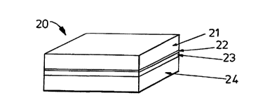
shown in Figure 19. The waveguide is an Anti-Resonant Reflecting Optical
CA 02321891 2000-08-23
WO 99/44042 PCTlGB99100399
23
Waveguide (ARROW). ARROW's are a class of waveguide which exhibit special
propagation characteristics that make them suited to optical sensing
applications.
ARROW waveguides were first developed in 1986 at AT&T Bell labs, and are
described in the paper: Duguay et al, Appl. Phys. Lett., 49 (1986) 13-15. The
waveguide 20 shown in Figure 19 is an ARROW structure, and comprises a sensing
layer 21 (approx. 4 p.m) of low refractive index gel (or other low index
substance of
interest) situated on top of a thin high index layer 22 (approx. 0.1 pm),
which in turn
is located on top of a layer of silica 23 (approx. 0.5 Vim). The entire
structure is
supported on a transmissive substrate 24 (for example glass). Light
propagating in the
sensing layer 21 of the waveguide 20 will undergo total internal reflection at
an
interface between an upper surface of the sensing layer 21 and the surrounding
air or
other low index medium, and undergo very high reflection from high index layer
22.
The high index layer 22 acts as a Fabry-Perot resonator at anti-resonant
wavelengths,
providing a very high degree of confinement of the optical mode within the
sensing
layer 21.
It is within the sensing layer 21 of the waveguide 20 that molecular
interactions (or any other interactions) which are to be studied occur. The
waveguide
20 thus exploits an important advantage of ARROW structures, namely that they
allow concentration of an optical field in a low refractive index region of
interest.
This feature is important since biological sample separation, antibody-antigen
interactions etc. are usually carried out in low index dextran gel. The
waveguide 20
allows an optical field to be concentrated in the dextran gel (i.e. sensing
layer 21),
whereas in most known prior art waveguides the field is localised in a high
refractive
index layer adjacent to the dextran gel. The enhanced overlap in the waveguide
20
between the optical field and the region to be monitored provides
significantly
increased sensitivity.
The waveguide 20 is easy to fabricate, and dispersion characteristics of
ARROW modes are such that even a quite large variation in waveguide
parameters,
i.e. layer thickness or refractive index, does not significantly affect the
operation of
the waveguide. This is a significant advantage of the invention, since
conventional
known waveguides are very sensitive to variation of waveguide parameters.
CA 02321891 2000-08-23
r
~;VO 99/44042
24
PCT/GB99/00399
Figure 20 shows an optical sensing apparatus which utilises the waveguide 20
illustrated in Figure 19. The construction of the apparatus is based upon the
construction of the known resonant mirror biosensor (see Cush, R. et al (1993)
The
resonant mirror, Biosensois & Bioelectronics, 8, 347-353). The apparatus
comprises
a source 25 which produces a beam of light at a known wavelength. The beam is
collimated, and then polarised by a polariser 2G to provide equal proportions
of TE
and TM excitation before being focused into a prism 27. The beam is coupled
from
the prism 27 into the waveguide 20 via leakage of the modes of the waveguide
20.
Efficient coupling into the sensing layer 21 of the waveguide 20 will occur
only for
certain angles of incidence where phase matching between the incident beam and
resonant modes of the sensing layer 21 is achieved. The angle at which the
beam is
incident upon the prism 19 is scanned continuously through a predetermined
range,
which is chosen to include those angles needed to excite resonant modes of the
core
layer. An alternative arrangement of apparatus couples incident light to the
waveguide 19 in a wedge shape, thereby providing light simultaneously at a
range of
incident angles which include all angles of interest.
The incident angle which will provide efficient coupling to the sensing layer
21 of the waveguide 20 (i.e. the angle which will excite a mode of the
waveguide 20)
is dependent upon the refractive index of the sensing layer 21 and on the
refractive
index of the substrate 24 and prism 27. Molecular interactions occurring
within the
sensing layer 21 will modify the refractive index of the core 21 and thereby
change
the incident angle required for efficient coupling. This change in refractive
index may
be monitored by measuring changes in the angle which provides efficient
coupling.
Light which is coupled into the sensing layer 21 propagates a short distance
along it before coupling back into the prism 27. Light emitted from the prism
27 may
be collimated and then caused to pass through an analyser 28 comprising a
polariser
set at 45° to the axes of polarisation of the TE and TM components of
the light and a
quarter-wave plate. A detector 29 measures the position of fi-inges produced
by
interference beriveen the TE and TM components of the light passed by the
analyser
28.
The phase of light reflected by the waveguide 20. undergoes a full 2n change
on passing through a resonance peak (i.e. an angle of incidence which provides
CA 02321891 2000-08-23
C
WO 99/44042 PCT/GB99/00399
efficient coupling to the sensing layer 21 }. It is the position of this phase
step which
is monitored to measure changes in the optical properties of the sensing layer
21. The
resonant optical modes for TE and TM excitation are widely separated. As the
angle
of the incident light approaches the angle needed to excite, for example, a
resonant TE
mode, the phase of light coupled from the core layer will be shifted, and will
pass
through a maximum phase shift of n at the resonance peak. Light which is
coupled to
a TM mode of the sensing layer 21 at the same angle of incidence will not pass
through a resonant mode, and interference at the analyser between light
coupled from
the TE and TM modes of the sensing layer 21 will be modified by the n phase
shift of
the TE mode, thereby indicating the presence of the TE resonance.
The ARROW waveguide is advantageous over known optical sensing
apparatus in that the resonant modes of the waveguide 20 are almost wavelength
insensitive, thereby removing the need for coherent sources of light to be
provided
with wavelength stabilisation mechanisms.
The source 25 used by the ARROW waveguide may be either a laser, a light
emitting diode or a white light source. The use of a light emitting diode (or
a white
light source), which produces light over a wider band of frequencies than
would be
produced by an equivalent laser, is made possible by the wavelength
insensitivity of
the ARROW structure of the waveguide 20. Light emitting diodes and other broad
band sources ate advantageous because they do not suffer from 'speckling',
which
degrades the performance of instruments that use diode lasers. The use of a
white
light source will allow the spectroscopic analysis of biological samples -
something
that is difficult or impossible to do with conventional waveguide sensors.
The ARROW waveguide is advantageous in that the method of excitation of
modes of the ARROW waveguide and the method of detection is the same as is
currently used for RM modes in the known resonant minor biosensor (see Cush,
R. et
a~. ARROW waveguides may therefore be used in place of resonant minor
waveguides in existing apparatus to obtain enhanced measurement sensitivity,
witheut
requiring a substantial change of instrumentation.
Figure 21 shows the real part of the amplitude of an optical field in the
waveguide of Figure 19. For comparison, two modes of the waveguide are shown:
a
resonant mode which occurs when the waveguide is acting as a resonant mirror,
and a
CA 02321891 2000-08-23
PCT/GB99/00399
WO 99/44042
26
mode which occurs when the waveguide is acting as an ARROW waveguide. From
Figure 21 it can be seen that the overlap between the ARROW mode and the
sensing
layer 21 of gel is almost 100% whilst the overlap of the resonant mirror (RM)
mode
and the sensing layer 21 is about 40%. Any change in the refractive index of
the gel
of sensing layer 21 therefore has a greater effect on the ARROW mode than it
does on
the RM mode. The ARROW mode thus provides more sensitive detection than the
RM mode, thereby providing the sensing apparatus with an enhanced performance
when compared to RM sensors.
A further advantageous feature of the ARROW waveguide is that the leakage
rate associated with the ARROW mode is much lower than that associated with
the
RM mode. This means that the ARROW mode resonances are much sharper than RM
resonances (although the leakage rate of RM modes can be reduced by increasing
the
thickness of the silica layer 23).
The shift in the resonance angle of an ARROW resonance in response to a
change in the refractive index of the core 21 was found to be 1.8 times
greater than
that of the corresponding RM resonance. With a tuned ARROW structure however,
this figure may be increased to over 12. This enhanced shift of resonance
angle,
together with the relative sharpness of the ARROW modes, allows the sensing
apparatus comprising an ARROW waveguide to resolve much smaller changes in the
refractive index of a core layer than may be measured using conventional RM
sensors.
A large overlap between the optical field and a core layer is a pre-requisite
for
efficient fluorescence and absorption measurements. The ARROW w~aveguide
provides this large overlap. Since the overlap between the A.R.ROW mode and
the
sensing layer 21 is almost 100%, the ARROW waveguide is particularly suited to
fluorescence and absorption measurements.
The silica layer 23 in the waveguide of Figure 19 is included so that both
resonant minor modes and ARROW modes of the waveguide 20 may be excited,
thereby allowing comparisons of their properties. However, it is possible to
fabricate
~ SOW waveguide which does not include the silica layer 23. A waveguide of
this form will be unable to support resonant mirror modes, but will support
ARROW
modes in the manner described above.
CA 02321891 2000-08-23
dV0 99/44042 PCTlGB99/00399
27
Although in general it is advantageous to produce waveguides which suffer as
little absorption loss as possible, losses suffered by light in an ARROW
waveguidc
mode may be of some use. Specifically, when a mode of an ARROW waveguide is
excited, absorption suffered by the light in the waveguide mode will reduce
the
intensity of light coupled from the waveguide, when compared to light which is
not
coupled to a resonant mode of the waveguide. Thus, the presence of an ARROW
mode will be indicated by a dip in the intensity of light coupled from a
waveguide.
Since a mode may be detected as a change of intensity rather than as a change
of phase, the angle of resonance may be determined without using the polariser
26 or
analyser 28. The size of the dip in the intensity of light coupled from the
waveguide
is a function of the losses suffered by the mode in the waveguide, either by
absorption
or scattering. A disadvantage of absorption losses is that they will broaden
resonances
of an ARROW waveguide, thereby reducing measurement sensitivity.
Optical absorption losses may be induced by introducing absorbing dyes
within the core and/or high index layers. Equivalent losses may be induced by
providing a degree of roughness to one or more of the surfaces of the core or
high
index layers.
For a given set of waveguide parameters there is an optimal value of thickness
of the high index reflector (layer 22 in Figure 19), at which the leakage rate
for a
particular ARROW mode is a minimum. Minimising the leakage rate will reduce
the
width of the ARROW resonance to a minimum (the ARROW resonance is the range
of angles of incidence which excite the ARROW mode). In many cases, it is
advantageous to minimise the width of the ARROW resonance, since this will
maximise measurement sensitivity.
A simple ARROW structure with a refractive index proftle is shown in Figure
22. The reference numerals of Figure 22 correspond with the reference numerals
applied to the structure shown in Figure 19. For a structure of this type, the
value of
the optimum thickness, t, of the high-index reflector layer is given to a good
approximation by: '
_ (2N + 1).?. _n,
4n, 1 ~n,~ + 4nZd2.
_ 2
CA 02321891 2000-08-23
PCT/GB99/00399
WO 99/44042
28
N: zero or a positive integer
free-space wavelength
n I : refractive index of the core (guiding layer)
n2: refractive index of the high-index reflector layer
d: thickness of the core (guiding layer}
For the simple ARROW waveguide shown, this formula gives a good
approximation to the optimum value of t, i.e. the value that results in a
minimum
leakage rate. A fundamental mode of a simple ARROW structure with the
refractive
index profile shown in Figure 22 is illustrated in Figure 23.
However, because the structure of ARROW sensors will not generally be as
simple as that shown in this example, the value of t obtained by this formula
can be
taken as a rough guide only. To determine the optimum value of the reflector
thickness for any general ARROW structure, the ARROW mode index may be
numerically determined, e.g. by the transfer matrix method. The set of
waveguide
parameters that give the lowest leakage rate can then be determined.
In an alternative configuration of waveguide, the thicknesses and refractive
indices of the high index layer 22 and the substrate 24 is selected to act as
a Fabry-
Perot resonator at resonant wavelengths (i.e. the thickness of the high index
layer 22 is
a multiple of the wavelength of light coupled to the waveguide, such that a
maximum
or near-maximum leakage of the optical mode occurs). This is in contrast to
the
design of ARROW waveguides, in which the structure is chosen such as to
minimise
the leakage of the optical mode. The waveguide configuration, referred to
hereafter as
a ROW waveguide provides strong confinement of light in the sensing layer 21.
A feature of suitably tailored ROW waveguides is that the mode index is a
strong function of the refractive index of the sensing layer 21. The mode
index of the
sensing layer 21 is generally referred to as (3, and the refractive index of
the sensing
i
layer 21 is generally referred to as 'n'. In ARROW waveguides, the quantity
d~3/dn is
approximately 1Ø However, in properly tailored ROW waveguides, d(3/dn may be
significantly larger than 1Ø In other words, a change of the refractive
index of the
CA 02321891 2000-08-23
WO 99/44042 PCT/GB99/00399
29
sensing layer 21, for example as the result of a molecular interaction, will
in general
lead to a larger change in the optical properties of the guided mode than
would be
seen in an ARROW waveguide.
A drawback or ROW waveguides is that the mode index of ROW modes is a
strong function of not only the refractive index of the sensing layer 21, but
also of the
refractive index and thickness of all other regions of the waveguide
structure.
Fabrication tolerance is therefore much stricter for ROW waveguides than it is
for
ARROW waveguides. Another drawback of ROW modes is that the mode index is a
function of optical wavelength, and monochromatic optical excitation of ROW
modes
is this usually necessary. The main advantage of ROW waveguides is that the
enhancement in sensitivity to changes of optical properties of a sensing layer
21 can
be very large. In the ROW structure used as an example below, the value of
dp/dn is
modest (approximately 1.09, compared with approximately 1.0 for ARROW
waveguides). With suitable design, this value can be much higher
A ROW waveguide structure is illustrated in Figure 24. The structure
comprises the following layers:
LayerRefemnceNo.Region Refractive indexThickness (microns)
30 Superstrate1.00
31 Sensing 1.347 or 1.3471 4.0
layer
32 Silicon 2.00 0.17
nitride
33 Silica 1.47 1.0
34 Metal 0.13 - i3.16 0.015
35 Substrate 1.72038
The waveguide structure shown in Figure 24 has been computer modelled and
found to operate as a ROW waveguide for light of 660nm. When the refractive
index
of the sensing layer 31 is 1.3470, the real part of the mode index of the TE,
is
1.344562. When the refractive index of the sensing layer 31 is 1.3471, the
real part of
the mode index of the TEZ is 1.344671. This gives a value of d~/dn=1.09.
The metal layer 34 is included in the waveguide structure merely to provide
optical loss and thereby allow the modes to be detected. as dips in the
intensity of
CA 02321891 2000-08-23
WO 99/44042 PCT/GB99/00399
reflected light. The ROW wavegui,de structure in general does not require a
layer of
metal.
A mode profile of the TEZ ROW mode is shown in Figure 25.
The preceding discussion and the following discussion of ARROW waveguide
structures may be applied, with relevant change, to ROW waveguide structures.
A broad resonance may be obtained from an ARROW structure by detuning
the waveguide structure from the optimal ARROW configuration. This can be done
by adjustment of any one or any combination of the following parameters:
thickness
of the high index layer, refractive index of the high index layer, refractive
index of the
substrate, refractive index of the sensing layer, thickness of the sensing
layer,
wavelength of the incident light.
If, on the other hand, it is required that the ARROW resonance be sharper than
that obtained using the optimal structure, further high index reflector layers
may be
included in a waveguide. Any number of high index reflector layers may be
included
in a waveguide structure. The refractive index profile of an ARROW waveguide
which includes two high refractive index layers is shown in Figure 26. The
waveguide comprises a substrate 36 on top of which is provided two high
refractive
index layers 37, 38 separated by a spacer layer 39. A sensing layer of gel 40
is
located on top of the uppermost high index layer 38. An upper surface of the
sensing
layer 40 forms an interface with a superstrate 41 of, for example, air. The
refractive
indices and thicknesses of the various layers of the waveguide shown in Figure
26
may be varied in order to achieve a desired sharpness of ARROW resonance. The
thickness and/or the refractive index of the high index layers 37 and 38 need
not be
the same. The refractive index of the sensing layer 40 must be greater than
that of the
superstrate 41, but less than that of the high index layer 38.
A further alternative form of ARROW waveguide structure is illustrated in
Figure 27. In this structure, a sensing layer 42 is bounded on either side by
a high
index layer 43, and a substrate 44. The structure illustrated in Figure 27
v~ill be
referred to as symmetric, to differentiate it from those structures described
above,
which are grouped together under the description 'asymmetric'. In asymmetric
ARROW waveguides, an uppermost surface of a sensing layer is bounded by a~semi-
infinite medium of lower refractive index (for example, air or water), which
boundary
CA 02321891 2000-08-23
WO 99/44042 PCT/GB99/00399
31
provides total internal reflection. By contrast, a sensing layer 42 of a
symmetric
ARROW waveguide is bounded on two sides by a high refractive index layer 43
and a
substrate 44, which form two ARROW structures, oriented such that modes in the
sensing layer 42 are confined on both sides by ARROW confinement. The word
'symmetric' is intended to mean that the sensing layer 42 is provided on both
sides
with an ARROW structure, and does not require that the refractive indices of
equivalent layers on either side of the sensing layer 42 are identical, or
that the form
of the ARROW structure on either side of the sensing layer 42 be the same.
A feature of symmetric ARROW sensors is that, as well as reflection of
incident light, they also provide transmission of incident light. This is not
the case
with asymmetric ARROW sensors, in which transmission of light is inhibited by
total
internal reflection at an uppermost surface of a sensing layer. In contrast to
this,
ARROW modes in symmetric ARROW waveguides are leaky on both sides of the
sensing layer 42. However, if desired, even a symmetric ARROW structure can be
designed such that the ARROW modes are leaky on only one side. This may be
achieved by reducing the refractive index of a superstrate of the structure to
below the
mode index of the ARROW modes of interest.
Transmission of light by a symmetric ARROW waveguide will occur only
when light is incident on the waveguide at a resonant angle. The fact that a
svmmetnc
ARROW waveguide will transmit as well as reflect light greatly simplifies the
measurement of the angle of incident light required to excite a resonance of
the
ARROW waveguide. An apparatus similar to that shown in Figure 20 may be used
with unpolarised light, thereby removing the need for polarisers at the input
and
output sides of the waveguide. At ARROW resonance angles, there is a dip in
the
reflectivity and a peak in the transmissivity of the waveguide,.either of
which may be
detected easily. The position of the transmissivity peak is measured using a
prism on
the transmission side of the waveguide, and a detector.
A construction of symmetric ARROW waveguide with a sensing layer
consisting of fluid may be used to detect refractive index changes in~ that
fluid.
Changes of the refractive index of the fluid are monitored using the
techniques
described above.
CA 02321891 2000-08-23
PC'T/GB99/00399
CVO 99144042
32
Alternative techniques for coupling light into an ARROW waveguide
according to the invention include end-fire coupling and coupling via a
grating etched
on an interface within the waveguide.
Although the invention has been described by way of example in ternis of
simple ARROW waveguides, it will be clear to those skilled in the art that
alternative
more complicated configurations of ARROW waveguide may be fabricated which
also allow an optical mode to be confined in, for example dextran gel or a
polymer.
Examples of such waveguides which may be used as pan of an optical sensing
apparatus are Directional-Couplers, Mach-Zehnder and other interferometric
devices.
Figure 28 shows a waveguide according to the sixth aspect of the invention,
which waveguide is referred to hereafter as a light condenser. The light
condenser
comprises a high index superstrate 45, a low index sensing layer 46 and a high-
index
substrate 47. One possible configuration of a light condenser comprises a low
index
gel or other medium of interest with a refractive index of n = 1.333,
sandwiched
between two layers of glass. The light condenser is a simple low-index
waveguide
with properties similar to ARROW waveguides.
Light is confined in the low-index guiding region of a light condenser by
reflection from the index steps between the low-index sensing layer 46 and the
high-
index superstrate 45 and substrate 47. Because the refractive index of the
superstrate
45 and substrate 47 is higher than that of the sensing layer 46, modes of the
light
condenser are leaky in nature. In other words the reflection from the core-
cladding
boundary is less than 100%, as indicated by light shown as arrows escaping
through
the superstrate 45 and substrate 47.
The guiding layer may be a polymer, water, gel or any other low-index .
material whose refractive index is to be monitored or in which fluorescence is
to be
excited.
The waveguide will function as a light condenser provided that the real part
of
the mode index of the light condenser mode is less than the refractive index
of the
superstrate 45 and substrate 47. ~ '
Figure 29 shows a waveguide in which the refractive index of a substrate 48 is
greater than the refractive index of a sensing layer 49, and the refractive
index of the
superstrate SO is less than the refractive index of the sensing layer 49.
Light is
CA 02321891 2000-08-23
PCT/G B99/00399
WO 99/44042
33
confined at the interface between the sensing layer 49 and the substrate by an
index
step, as described in relation to Figure 28. Light is confined at the
interface between
the sensing layer 49 and the superstrate 48 by conventional total internal
reflection. A
waveguide of this type will be referred to as an asymmetric light condenser.
In the
asymmetric light condenser the real part of the mode index of a light
condenser mode
of interest is generally greater than the refractive index of the superstrate
48.
The waveguide will function as a light condenser at the interface between the
sensing layer 49 and the substrate 48, provided that the real part of the mode
index of
the light condenser mode is less than the refractive index of the substrate
48.
The method of excitation of light condenser modes is the same as that
described in relation to ARROW modes, and may utilise for example prism
coupling,
grating coupling or end-fire coupling.
The light condenser does not generally require lateral mode confinement, since
light coupled to the light condenser is collimated. Where lateral confinement
is
required, this may be provided by etching into a substrate or superstrate a
channel for
receiving a sensing medium.
The light condenser waveguide may be fabricated from injection moulded
plastic. A coupling prism may be formed together with the light condenser
during
fabrication. Electrodes, if required, may also be formed together with the
light
condenser during fabrication.
The light condenser waveguide may be used in the measurement of
fluorescence (by including a fluorescent species in the sensing layer).
Figure 30 shows a resonant mirror waveguide structure designed to operate at
a wavelength of 0.66 microns, and designed to provide a measurement and a
reference
for that measurement. The waveguide structure comprises a sample 51 provided
as a
sensing layer on top of a thin layer of silicon nitride 52 (80nm), which in
turn is
located on top of a thick layer of silica 53 (SOOnm). The silica layer is
located on a
second thin layer of silicon nitride 54 (100nm), which is located on a second
thick
silica layer 55 (SOOnm). The entire structure is located on a substrate 56'
(the
undersides of which are angled to form a prism). The illustrated waveguide
structure
essentially comprises a first resonant mirror structure located on top of a
second
resonant mirror structure. The sensing layer may be low index dextran gel, or
may be
CA 02321891 2000-08-23
PCTIGB99/00399
WO 99/44042
34
any other medium capable of supporting biological or chemical interactions,
for
example sample separation, antibody-antigen interactions, etc.
An optical sensor according to the invention is shown in Figure 31. The
sensor is similar to existing apparatus which is used to perform resonant
mirror
measurements and surface plasmon resonance measurements but modified to
incorporate the waveguide structure of Figure 30. The apparatus according to
the
invention comprises a light source 57 which produces a beam of light at a
known
wavelength. A polarises 58 is arranged to provide equal proportions of TE and
TM
excitation, and a lens 59 focuses the beam to a fan-shape. The beam is
directed into a
prism 56 which forms part of the waveguide. Although the prism 56 is shown as
being triangular, it could be of any suitable shape (for example rectangular),
and other
forms of substrate may be used. Because the beam is directed towards the
waveguide
as a fan, light is incident at the waveguide from a range of different angles.
The
incident light will either be coupled to two resonant minor modes centred
respectively
on the layers of silicon nitride 52, 54 or will be reflected from the
waveguide structure
without being coupled to a resonant minor mode. Light will be coupled from the
prism 56 of the waveguide in the form of a fan, and, after passing through a
collimating lens 60 and an analyser 61 (comprising a polarises and a quarter-
wave
plate), will be incident upon a detector 62. The detector 62 comprises an
array of
charge coupled devices (CCD's) which detect the intensity of light at
different
sections of the fan, i.e. at different incidence angles.
The phase of light coupled from the waveguide will undergo a full 2n change
on passing through a resonance peak (i.e. an angle of incidence which provides
efficient coupling to the modes centred on the layers of silicon nitride 52,
54). It is
the position of these phase changes which is monitored to measure changes in
the
optical properties of the sample 51. The resonant mirror optical modes for TE
and
TM excitation are widely separated in incidence angle. As the angle of the
incident
light approaches the angle needed to excite, for example, a resonant TE mode
centred
on the first layer of silicon nitride 52, the phase of light coupled from the
waveguide
will be shifted, and will pass through a maximum phase shift of n at the
resonance
peak. Light which is coupled to a TM mode of the same layer at the same angle
of
incidence will not pass through a resonant mode. The polarises 60 is arranged
to mix
CA 02321891 2000-08-23
WO 99/44042 PCT/GB99/00399
light from the TE and TM modes, thereby providing interference which passes
through a peak of intensity as the TE mode passes through resonance. The
position of
the peak of intensity is dependent upon the optical properties of the
waveguide
structure.
The CCD array of the optical sensor may be replaced by a pair of photo-diodes
(not shown) mounted so as to be capable of translation in a direction
perpendicular to
the direction of the light reflected from the waveguide. In use the photo-
diodes would
be positioned where peaks of intensity occurred, and would be translated to
follow the
peaks of intensity during an experiment, thereby allo~~ing measurement of the
degree
of movement of those peaks of intensities.
It will be appreciated that the combination of the light source ~7 and lens 59
of
Figure 3I may be replaced by a collimated light source, mounted on a swinging
arm.
The arm would be swung through a required range of angles to produce
illumination
at the waveguide similar to the fan of light shown in Figure 31. The lens 59
would
not be required by the swinging arm arrangement.
The lens 60 may be removed from the apparatus without significant loss of
performance.
Since the waveguide structure comprises two resonant mirror waveguides, a
first angle of incidence will excite a mode centred on the first layer of
silicon nitride
52 (i.e. a mode of the first resonant mirror), and a second angle of incidence
will
excite a mode centred on the second layer of silicon nitride 54 (i.e. a mode
of the
second resonant mirror).
Figures 32 and 33 illustrate optical fields associated with modes centred
respectively on the first and second silicon nitride layers (52, 54) of the
waveguide
structure of Figure 30 (the reference numerals are as used in Figure 30). A
significant
fraction of the mode illustrated in Figure 32 extends into the sensing layer S
1 of the
structure, and this mode will therefore be affected by changes of the optical
properties
of the sensing layer 51 (this mode will be referred to as the measurement
mode). In
contrast, only a very small proportion of the mode illustrated in Figure 33
extends~into
the sensing layer 51, and this mode will be largely unaffected by changes of
the
optical properties of the sensing layer 51 (this mode will be referred to as
the
reference mode).
CA 02321891 2000-08-23
WO 99/44042 PCT/GB99/00399
36
Using the structure of Figure 30 it is possible to differentiate behveen
changes
in optical properties of the sensing layer 51, and unwanted optical effects
such as any
variation of the wavelength of light incident on the waveguide structure. For
example, if the wavelength of incident light was to change, the angles of
incidence
required to excite both the measurement and reference modes would be altered,
and
the positions of the corresponding measurement and reference peaks detected by
the
CCD camera would be altered. The change in position of the reference peak is
determined, and subtracted from the position of the measurement peak to remove
the
effect of the wavelength change from the measurement. This is illustrated in
the
experimental result shown in Figure 34. The peaks on the graph are the
recorded
positions of outputs from an optical sensor incorporating the waveguide
structure
,:.' . _
shown in Figure 30, for four different wavelengths of incident light. Thepeaks
63 af~
the left-hand end of the graph are measurement peaks, and the peaks 64 to the
right-
hand end of the graph are reference peaks. From Figure 34, it is clear that
both the
measurement and reference modes (and the positions of the corresponding peaks)
are
affected similarly by the changes of wavelength.
In contrast, a change of the refractive index of the sample comprising the
sensing layer 51 will significantly affect only the mode shown in Figure 32.
This is
illustrated in Figure 35, where the positions of the measurement peaks 65 to
the left-
hand end of the graph vary as the refractive index of the sample comprising
the
sensing layer 51 changes, and the reference peaks 66 to the right-hand end of
the
graph are substantially unaffected. '
The invention is advantageous because it removes the need for stabilisation of
the wavelength of the incident light; the effect of wavelength variation being
removed
by comparison of the measurement and reference peaks. A further advantage of
the
invention is that measurements are unaffected by changes in the temperature of
the
waveguide structure. If the temperature of the waveguide structure was to
change,
this would affect the measurement and reference modes equally, and the effect
of the
temperature change would thus be eliminated by comparison of the measurement
'and
reference peaks.
In the above description it has been assumed that effects which act on both
the
measurement and reference modes (for example a change of wavelength) will
affect
CA 02321891 2000-08-23
WO 99/44042 PCT/GB99/00399
37
each mode equally. However, since the modes are not identical, each mode will
in
fact behave slightly differently. By calibrating the effect of wavelength and
temperature variations when the sample comprising the sensing layer 31 is
inactive,
the accuracy of subsequent measurements may be maximised. In the alternative,
doping may be introduced into the structure in such a manner as to ensure that
measurement and reference modes have the same behaviour with respect to
temperature and wavelength variations.
The thickness of the first layer of silica 53 (in the waveguide shown in
Figure
30) is of importance to the operation of the invention. If this layer is too
wide then the
measurement mode will not be excited, and if the layer is too thin then the
reference
mode will extend too far into the sensing layer 51, and will not provide a
reference
substantially independent of the sensing layer 51. The thickness of the first
silicon
nitride layer 52 may be chosen to be slightly less than the thickness of the
second
silicon nitride layer 54. This is so that the first layer is slightly more
'leaky' Lhan the
second, thereby ensuring that a sufficient proportion of the measurement mode
will
penetrate into the sensing layer 51.
Figure 36 illustrates an anti-resonant reflecting optical waveguide (ARROW)
biosensor, which is capable of supporting a reference mode which is unaffected
by
changes in the optical properties of a sample. The ARROW structure is
comprised of
the following layers:
Laver Ref~e Material Refractive Thiclmess (microns)
No. Index
67 Substrate (SF 1.72038 Semi-infinite
10)
68 Silica 1.47 0.55
69 Silicon Nitride2.00 0.08
70 High-Index 1.65 3.00
Layer
71 Silica 1.47 0.55
72 Silicon Nitride2.00 0.08
73 Dextran Gel 1.35 3.00
74 Water 1.333 I Semi-infinite
CA 02321891 2000-08-23
.WO 99/44042
38
PCT/GB99/00399
It will be understood that the above materials and thicknesses are given only
as
examples, and other materials of appropriate thicknesses may be used to
construct a
waveguide capable of supporting ARROW modes. In particular, the dextran gel is
just one of many possible materials which may be used to support a sample of
interest. The layer of substrate may be considered to be semi-infinite, and
the
substrate is shown as being 1 micron thick to allow a zero position to be
defined.
Figures 37 and 38 respectively show first and second ARROW modes centred
on layers 73 and 70 of the structure of Figure 36. The modes are excited by
directing
incident light from an appropriate angle, in a manner analogous to that
described
above. The physics of ARROW waveguides is well known, and is described in the
paper: Duguay et al, Appl. Phys. Lett., 49 (1986) 13-15. The reference mode of
the
ARROW waveguide (i.e. the second mode), as shown in Figure 38, may be used to
eliminate unwanted artefacts from a measurement of the optical properties of a
sample, in the manner described above.
It will be understood by those skilled in the art that the waveguide structure
illustrated in Figure 36 may also be made to support resonant mirror modes.
The
silica layers 68, 71 are included in the waveguide to allow the resonant
mirror modes
to be supported. This particular waveguide is designed to support resonant
mirror
modes at a wavelength of 0.66 microns. A waveguide constructed without these
layers would not support resonant mirror modes, but would still be capable of
supporting ARROW modes.
Figure 39 illustrates a further embodiment of the invention. A waveguide
comprises a prism 75, a layer of silica 76 and a high index silicon nitride
layer 77. A
layer of chemically inert material 78 with a refractive index. lower than that
of the
silicon nitride layer 77 is located at a left hand end of an upper surface of
the silicon
nitride layer 77, and a sample 79 is disposed as a sensing layer so as to
cover the
remaining upper surface of the silicon nitride layer 77 and an upper surface
of the
polymer layer 78.
In use, when a fan of light is coupled into the waveguide of Figure 39, a mode
centred on the silicon nitride layer 77 will be excited. At a left hand end of
the
waveguide the mode will extend into the polymer layer 78, but will not extend
substantially beyond the polymer layer 78. At a right hand end of the
waveguide the
CA 02321891 2000-08-23
CVO 99/44042
39
PCT/GB99100399
mode will extend into the sensing layer 79. Thus, the excited mode comprises
two
components which may be considered to be two modes, the left hand mode being
substantially unaffected by changes of the properties of the sample (i.e. a
reference
mode) and the right hand mode being sensitive to changes of the properties of
the
sample (i.e. a measurement mode). The waveguide shown in Figure 39 may be used
with the apparatus shown in Figure 31, as described above.
It will be understood that the layer of silicon nitride 77 could be replaced
by a
layer of any suitable material having a refractive index greater than that of
the silica
76, the inert material 78 and the sensing layer 79. Similarly, the layer of
silica may be
replaced by any other suitable material. The chemically inert material 78 may
be
silicon, or alternatively a polymer chosen because it does not react to an
analyte to be
monitored may be used.
Figure 40 shows a first resonant mirror mode located at a right hand end of
the
waveguide structure of Figure 39. A substantial proportion of the first mode
extends
into the sensing layer 79, and this mode will therefore be sensitive to
changes of the
optical properties of that layer (i.e. the first mode is a measurement mode).
Figure 41 shows a second resonant minor mode located at a left hand end of
the waveguide structure of Figure 39. Only a very slight proportion of the
second
mode extends into the layer of sensing material 79, and this mode will
therefore be
substantially unaffected by changes of the optical properties of that layer
(i.e. the
second mode is a reference mode).
The waveguide of Figure 39 is advantageous over previously described
embodiments because it has fewer layers and is therefore easier and cheaper to
fabricate.
It is noted that the substrate of the above waveguide structures described in
Figures 30, 36 and 39 (i.e, layers 56, 67 and 75) may be angled to form a
prism, or
may be provided with a planar base which is to be located upon a separate
prism made
from the same material as the substrate.
Each of the waveguide structures described in Figures 30, 36 and ~9 may also
be provided in what is known as a symmetric form. In each case the symmetric
form
comprises a central layer of sensing medium, with identical layers disposed on
either
side of the central layer, the layers on both sides being arranged as shown in
Figures
CA 02321891 2000-08-23
C
.WO 99/44042 PCT/GB99100399
30, 36 and 39. Light coupled to a symmetric waveguide v,~ill undergo
reflection as
described above, but will also be transmitted by that waveguide when a
resonant
mirror mode or A.R.ROW mode is excited. The proportion of light reflected by
the
waveguide when a resonant mirror mode or ARROW mode is excited is reduced as a
consequence of the transmission, and the presence of such a mode will
therefore
indicated by a dip in the intensity of light reflected by the waveguide.
Symmetric
arrangements of waveguides are thus advantageous because they allow the
detection
of resonant mirror modes or ARROW modes without the use of polarisers or wave-
plates.
Detection of resonant mirror modes or ARROW modes may also be achieved
by introducing absorption or scattering loss into the layer of sensing medium
of the
waveguide structures shown in Figures 30, 36 or 39. In a waveguide of this
type
excitation of a resonant minor mode or ARROW mode will lead to a reduction of
the
intensity of light reflected from the waveguide, due to losses occurring in
the sensing
medium. The presence of a resonant mirror mode or an ARROW mode will thus be
indicated by a dip in the intensity of reflected light. The introduction of
loss into the
sensing medium is advantageous because it simplifies detection, as discussed
above in
relation to the symmetric waveguide form. It is noted that the presence of
loss in the
sensing medium will increase the range of incidence angles which are capable
of
exciting a resonant mirror mode or ARROW mode, thereby reducing experimental
sensitivity.
The sensor waveguides described in relation to Figures 30 to 41 are similar in
terms of dimensions and optical properties to sensor waveguides used in
existing
resonant mirror optical biosensing apparatus. A sensor waveguide as descried
may
therefore be introduced into existing biosensing apparatus with a minimal
amount of
modification. The temperature stabilisation and current stabilisation used by
existing
biosensing apparatus is not required when sensors according to the invention
are used,
and may be dispensed with, thereby reducing the complexity and cost of the
apparatus. ~ .
It will be understood that the structures described in relation to Figures 30,
36
and 39 are concerned with providing waveguide structures having reference
modes
which are unaffected by changes of optical properties of a sample. The
invention may
CA 02321891 2000-08-23
WO 99144042 PC'f/GB99/00399
41
be applied to other waveguide structures, and such applications will be
apparent to
those skilled in the art.