Note: Descriptions are shown in the official language in which they were submitted.
CA 02322267 2000-10-04
,,. ,
1
Wt 14 US
Ke/Lo
14.10.99
Signal-Identifying Circuit Arrangement
This invention relates to a circuit arrangement for
identifying classified signals.
By means of industrial measurement devices, measurands,
such as pH value, pressure, temperature, or tank-contents
level, are converted into measured-value-carrying
electric measurement signals. To accomplish this, the
measurand is sensed by means of suitable sensing
elements, such as pH electrodes, pressures cells,
thermistors, or resistance strain gages, and modulated
onto a current component or a voltage component of the
measurement signal by means of suitable measurement
electronics, such as a resistance bridge. Since sensors
can be used only over respective limited measurement
ranges of the measurand, the measured values are also
represented in a limited current or voltage range.
These current and voltage ranges are generally
standardized. Current-modulated measurement signals, for
example, are preferably used in a current range of
4 mA...20 mA. Other types of measurement signals familiar
to those skilled in the art are, for example, voltage-
modulated signals in a voltage range of 0 to 10 V.
To indicate, record, or further process the measured
values from the measurement signal and to determine
CA 02322267 2000-10-04
f ,
2
corresponding measurement results, the measurement
devices are followed by analog and/or digital signal-
processing units, to which the measurement signal is fed
through suitable signal-matching input circuits.
If the measured value is modulated on the current of the
measurement signal, the signal-matching input circuit is
adjusted to operate in a current-sensing mode, and if the
measured value is modulated on the voltage of the
measurement signal, the input circuit is adjusted to
operate in a voltage-sensing mode. Furthermore, it is
usual to use such input circuits to implement a signal
preprocessing dependent on the type of the measurement
signal, e.g., to amplify and/or filter the measurement
signal. To accomplish this, during start-up, the
respective input signal must be adapted to the respective
current or voltage range to be represented.
The setting and adapting of the signal-processing unit
can be very time-consuming, particularly if the signal-
processing unit receives output signals from two or more
measurement devices simultaneously; this may entail very
high downtime and start-up costs. In addition, the
setting of the signal-processing unit requires exact
knowledge of the type of the measurement signals at the
measuring points to be connected.
Accordingly, sufficiently fast start-ups necessitate
complicated presettings, particularly of the input
circuit, i.e., start-ups of such signal-processing units
at short notice are practically impossible. In the case
of transportable signal-processing units, repeated start-
ups are necessary, involving a correspondingly greater
expenditure of time and money.
CA 02322267 2003-11-05
78254-4
3
It is therefore an object of the invention to
provide a signal-identifying circuit arrangement for a
signal-processing unit which reduces the cost and
complication of starting up the signal-processing unit.
In one aspect of the invention, there is provided
a circuit arrangement for identifying an input signal
delivered from an external measurement device, said input
signal belonging to a predetermined signal class, said
circuit arrangement comprising: signal-matching electronics
for the input signal which generate an output signal
representative of a current component of the input signal
and/or a voltage component of the input signal; and signal
recognition electronics which derive from the output signal
a recognition signal representative of the predetermined
signal class of the input signal delivered from the
measurement device.
In a second aspect, there is provided a signal-
processing unit for processing at least one input signal
delivered from an external measurement device, said input
signal belonging to a predetermined signal class, said
signal-processing unit comprising: a circuit arrangement
being coupled to said measurement device at least
temporarily, wherein the circuit arrangement uses the input
signal delivered from the measurement device to generate a
recognition signal representing said predetermined signal
class of said input signal delivered from the measurement
device.
In a third aspect, there is provided a data-
gathering unit, comprising a signal-processing unit for
processing at least one input signal delivered from an
eternal measurement device, said input signal belonging to a
CA 02322267 2003-11-05
78254-4
3a
predetermined signal class, said signal-processing
comprising a circuit arrangement being coupled to said
measurement device at least temporarily, wherein the circuit
arrangement uses the input signal delivered from the
measurement device to generate a recognition signal
representing said predetermined signal class of said input
signal delivered from the measurement device.
In a first embodiment of the invention, the
circuit arrangement comprises setting electronics that
derive from the recognition signal a setting signal serving
to set and/or parameterize the signal-matching electronics.
In a second embodiment of the invention, the
circuit arrangement comprises a current source providing the
current component of the input signal.
In a third embodiment of the invention, the input
signal is an output signal from a measurement device.
In a fourth embodiment of the invention, the
circuit arrangement serves as a component of a data-
gathering signal-processing unit.
CA 02322267 2000-10-04
4
A basic idea of the invention is to use the signal-
processing unit in a signal environment of predetermined
signal classes and apply to it, particularly during
start-up of the circuit arrangement, an input signal
belonging to one of these signal classes and to determine
the signal class of the input signal, and thus identify
the input signal, by means of the signal recognition
electronics.
From the respective detected signal class, inputs for
adjusting the signal-matching electronics to operate in a
current- or voltage-sensing mode and, if necessary, for a
corresponding parameterization of the signal-matching
electronics are derived, which are implemented
automatically or semiautomatically in communication with
the user.
One advantage of the invention is that during start-up,
based on an identification of the input signal, the
circuit arrangement can be adapted to the input signal
automatically and, thus, within a very short time, so
that it can be changed to the measuring mode
correspondingly fast.
Another advantage of the invention is that during start-
up of the signal-processing unit, circuit arrangements
not in use, i.e., not having an input signal applied to
them, can be identified and, thus, deactivated.
Conversely, such circuit arrangements can be activated
later during operation of the signal-processing unit and
set in a corresponding manner.
The invention and further advantages will become more
apparent from the following description of embodiments
~
. CA 02322267 2000-10-04
when taken in conjunction with the accompanying drawing.
Like parts are designated by like reference characters
throughout the figures; if necessary for the sake of
clarity, reference characters that were already used are
5 omitted in subsequent figures. In the drawings:
Fig. 1 is a block diagram of a circuit arrangement
with signal-matching electronics and with
signal recognition electronics for identifying
an input signal;
Fig. 2 shows a development of the signal-matching
electronics;
Fig. 3 shows a subcircuit of the signal-matching
electronics;
Fig. 4 shows a preferred embodiment of the signal
recognition electronics; and
Fig. 5 shows a further development of the signal-
matching electronics.
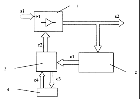
Fig. 1 is a block diagram of a circuit arrangement which,
as one component of a partly shown signal-processing
unit, particularly of a data-gathering unit, such as a
data storage device and/or a data display device, serves
to convert an applied information-carrying input signal
sl to an information-carrying first output signal s2,
particularly a digital signal, that can be further
processed by components following the signal-processing
electronics, particularly by evaluation electronics (not
shown).
The input signal sl is, for example, an electric output
signal, particularly an analog signal, from a measurement
device (not shown), such as a temperature meter, a
CA 02322267 2000-10-04
6
pressure gage, a flowmeter, a pH meter, or a level meter,
that transmits as information a measured value generated
by the measurement device or a parameter value
representative of the current operating state of this
measurement device. The input signal sl can also be an
output signal from another signal-processing unit (not
shown).
According to the invention, the circuit arrangement is
intended for use in a signal environment that provides
signals of different kinds serving as the input signal
sl, these signals being assignable to at least a first
predetermined signal class, such as a class for current
signals, and/or a second predetermined signal class, such
as a class for voltage signals. The term "signal
environment" as used herein means an ensemble of
different, classifiable signals for respective concrete
applications of the circuit arrangement which are
generated by means of suitable signal sources and fed to
the circuit arrangement, said ensemble being predefined,
particularly by the measurement devices used, and
arranged in individual signal classes.
Current signals are commonly generated as output signals
of a signal source, such as an amplifier circuit
configured as a voltage-controlled current source, which
delivers an essentially constant voltage that is
essentially independent of the magnitude of an
information-carrying current component, at least within a
predeterminable current range. By contrast, voltage
signals are commonly generated by means of a signal
source, such as an amplifier circuit configured as a
voltage-controlled voltage source, which delivers an
essentially constant current that is essentially
CA 02322267 2000-10-04
7
independent of the magnitude of an information-carrying
voltage component, at least within a predetermined
voltage range. Furthermore, the voltage-signal source can
be a resistor that is traversed by a predetermined
current and whose value is dependent on a process
quantity to be measured.
In signal environments of industrial measurement and
communications technology, the information carriers are
generally current signals in a current range of, e.g., 0
to 20 mA or 4 mA to 20 mA and voltage signals in a
voltage range of, e.g., 0 to 1 V, 0 to 10 V, 19 mV to 390
mV, or -10 mV to 80 mV. Each of these ranges is definable
as a predetermined signal class of this signal
environment.
Accordingly, prior to start-up of the signal-processing
unit, the circuit arrangement must be set depending on
the signal class of the respective input signal sl to be
transmitted so that the information will be mapped
uniformly onto the output signal s2 independently of the
information carrier, i.e., also independently of the
information-carrying current or voltage range. The output
signal s2 can be a voltage signal that represents the
information in a predetermined voltage range of 0 to 1 V.
As shown in Fig. 1, the circuit arrangement comprises
signal-matching electronics 1, particularly electronics
that are parameterizable in operation, with a first
signal terminal E1 for the input signal sl, particularly
a disable terminal, the signal-matching electronics 1
being settable to a mode in which it responds to a
current component/or a voltage component of the input
signal sl. The signal-matching electronics 1 can be
- . CA 02322267 2000-10-04
g
implemented, for example, with amplifier circuits of
predeterminable, particularly variable, gain and input
impedance that are configured as current-controlled or
voltage-controlled voltage sources. Such variable input
impedances and gains are commonly realized by means of
controlled impedance networks and/or by means of field-
effect transistors.
The circuit arrangement further comprises signal
recognition electronics 2, which deliver a quantized
recognition signal cl that is representative of the
signal class of the input signal sl and thus identifies
this signal. The signal recognition electronics 2 serve,
particularly during start-up of the signal-processing
unit, to classify the input signal sl changed to the
output signal s2, i.e., to assign this input signal sl to
a predetermined signal class, particularly to the first
signal class and/or the second signal class, and thus
identify this signal, particularly its information
carrier.
The recognition signal cl may consist of signal level
sequences of a single signal output of the signal
recognition electronics 2 or of an ordered sequence of
instantaneous signal levels of two or more signal outputs
of the signal recognition electronics 2. Particularly for
the latter case, each signal class can advantageously be
assigned a respective signal output, which can be used
for direct indication. If a number n of signal outputs
with binary levels is used, the recognition signal c1 can
assume 2°-1 different binary states, i.e., up to 2°-1
signal classes, for example, can be encoded with the
signal recognition electronics 2.
. CA 02322267 2000-10-04
9
If multiple-valued signal levels are used, particularly
in a normalized range of values greater than or equal to
logic ZERO and less than or equal to logic ONE, the
recognition signal cl can also serve to establish an
indeterminate, e.g., fuzzy-logic and/or probability-
induced, assignment of the input signal sl to the signal
classes. For this case, the input signal sl is
assignable, e.g. with a membership share of 0 to 100% per
signal class, to two or more signal classes
simultaneously, particularly as a function of
probabilities of occurrence determined a priori for the
signal classes of the respective signal environment.
The adjustment of the signal-matching electronics 1 to
operate, for example, in a current-component-sensing
and/or voltage-component-sensing mode takes place already
during the aforementioned start-up phase of the signal-
processing unit, namely in a timed mode and/or in an
event-driven mode, particularly in a dialog with an
interacting user.
To this end, the circuit arrangement comprises setting
electronics 3, which deliver a likewise quantized setting
signal c2. The setting signal is an ensemble of binary
and/or analog signal levels that are generated at signal
outputs of the setting elecronics 3 connected to
corresponding setting inputs or parameter inputs of the
signal-matching electronics 1.
The setting signal c2 serves, on the one hand, to adjust
the signal-matching electronics 1 temporarily,
particularly during the start-up phase of the signal-
processing unit, to operate in a current-component-
sensing and/or voltage-component-sensing mode as
- . CA 02322267 2000-10-04
described above, and to suitably parameterize them. On
the other hand, the setting signal c2 can also serve to
deactivate the signal-matching electronics 1 when no
input signal sl is applied or identified. Furthermore,
S the setting signal c2 can be used to parameterize signal
filters of the signal-matching electronics, particularly
of its filter arrangement and its upper and/or lower
cutoff frequencies. Such signal filters, particularly
first-order low-pass filters with an upper cutoff
10 frequency not greater than 5 Hz, are used, for example,
if thermocouple or resistance thermometers are connected
directly to the signal-matching electronics 1.
To implement the dialog with the user, the setting
electronics 3 derive from the applied recognition signal
cl an indication signal c3 that is representative of the
signal class of the input signal sl and serves to drive
an input-output unit 4 of the circuit arrangement.
Furthermore, the setting electronics 3 receive a control
signal c4 from the input-output unit 4 which is
representative of the user inputs. The input-output unit
4 can be a monitor with a touch screen/or with a
keyboard, for example. Advantageously, the recognition
signal cl can also serve to generate the setting signal
c2.
According to a development of the invention, shown in
Fig. 2, the signal-matching electronics 1 have a second
signal terminal E2 for the input signal sl, particularly
a disable terminal. The input signal s1 is an output
signal from a signal distributor module connected, at
least temporarily, to the signal-matching electronics 1,
e.g., a terminal strip and/or plug connector strip
following the above-mentioned measurement device. The
CA 02322267 2000-10-04
11
signal distributor module is configured to apply the
input signal sl to the signal terminal E1 only if the
input signal sl is of the first signal class, e.g., a
current signal. Furthermore, the signal distributor
module is configured to apply the input signal s1 to the
signal terminal E2 only if the input signal sl is of the
second signal class, e.g., a voltage signal.
In another preferred embodiment of the invention, shown
in Fig. 3, the signal-matching electronics 1 comprise a
first amplifier circuit V1, to which the input signal s1
is applied through a variable first impedance Z1, e.g., a
resistor, having a smallest resistance value of
practically 0 ~, to an inverting amplifier input. The
amplifier circuit V1 is provided with a variable second
impedance Z2, which connects its output to the inverting
input. The input impedance of the amplifier circuit V1 is
variable by means of the impedance Z1, and the gain is
variable by means of the two impedances Z1, Z2.
In a further preferred embodiment of the invention, the
impedance Z1 is adjusted so that the input signal sl is
applied to the amplifier input over a path of practically
zero resistance, so that the signal-matching electronics
1 are configured to respond to a current component of the
input signal s1, particularly a component carrying the
information, and to map this current component onto the
output signal s2.
In another preferred embodiment of the invention, the
impedance Z1 is adjusted to a high value, e.g., to lk~ or
1M~. Thus, the signal-matching electronics 1 are
configured to respond to a voltage component of the input
signal s1, particularly a component carrying the
- . CA 02322267 2000-10-04
12
information, and to map this voltage component onto the
output signal s2.
In a further preferred embodiment of the invenion, the
impedance Z1 has a greatest resistance value of
practically infinity, whereby a practically open switch
is implemented at the input of the signal-matching
electronics 1.
In another preferred embodiment of the invention, the
signal-matching electronics 1 are so configured that
their output signal s2 represents simultaneously a
current component and a voltage component of the input
signal sl, particularly a ratio of the voltage component
to the current component. To this end, the signal-
matching electronics 1 include a current-component-
sensing second amplifier circuit. For this case, the
amplifier circuit vl is adjusted to operate in a voltage-
component-sensing mode.
To generate the recognition signal cl, in a preferred
embodiment of the invention, shown in Fig. 4, the signal
recognition electronics 2 comprise a feature stage 21,
which serves to transform the output signal s2 into an
ensemble of features representative of this output
signal. To this end, the feature stage 21 generates a
quantized feature signal cll, e.g., a signal quantized
bit by bit, i.e., divided into bits representative of the
features.
The feature signal cll preferably has at least a first
logic state if the input signal sl belongs to the first
signal class, and at least a second logic state if the
input signal sl belongs to the second signal class.
CA 02322267 2000-10-04
13
Furthermore, the feature signal cll preferably assumes at
least a third logic state if the input signal sl is
assignable neither to the first nor to the second signal
class.
To represent features, use can be made, for example, of
comparator circuits and/or fuzzy sets that are
implemented in programmable function memories,
particularly in an EPROM or EEPROM, of the feature stage
21, compare the output signal s2 with predetermined
reference values and/or reference functions, and deliver
binary logic comparison values and/or fuzzy logic
membership values at corresponding bits of the feature
signal c11.
As shown in Fig. 4, the feature stage 21 of the signal
recognition electronics 2 is followed by a classification
stage 22, which serves to interpret the feature signal
cll, i.e., to map predetermined bits of the quantized
feature signal cll onto the recognition signal cl and
thus identify the input signal sl.
In a further preferred embodiment of the invention, the
feature signal c11 is interpreted using an ensemble of
binary logic and/or fuzzy logic decision rules that
combine the features represented by the individual bits
of the feature signal c11. Such binary logic decision
rules can be represented, for example, by means of
combinational logic circuits and/or sequential logic
circuits that are realized in the signal recognition
electronics 2 by means of hard-wired circuits and/or by
means of computing routines implemented in a programmable
function memory, such as an EPROM or EEPROM, and which
deliver the recognition signal cl as a sequence of
. CA 02322267 2000-10-04
14
weighted binary signal levels, e.g., as a binary-coded
sequence. Fuzzy logic decision rules are also commonly
represented using computing routines implemented in a
programmable function memory. Furthermore, the feature
signal cll can be interpreted using so-called distance
classifiers, which determine and interpret its difference
from classified and stored feature-signal prototypes.
In a further preferred embodiment of the invention, a
likwise quantized setting signal c5, particularly a
digital signal, which serves to interpret the feature
signal cll and represents a current setting and/or a
current parameterization of the signal-matching
electronics 1, is applied to the classification stage 22.
This setting signal c5 is preferably generated by means
of the setting electronics 3, but it may also be provided
directly by the signal-matching electronics 1.
In a further preferred embodiment of the invention, the
input signal sl is a current signal and is assigned to
the first signal class. To identify the input signal sl,
a first logic state of the recognition signal cl, which
is representative of the first signal class and, thus, of
the current component serving as an information carrier,
is generated by means of the signal recognition
electronics 2. This is done by means of a first feature
implemented in the feature stage 21, which represents a
difference currently existing between the output signal
s2 and a current reference value, this current reference
value corresponding to a current strength of the input
signal sl of, e.g., 1 mA. The first feature is preferably
represented using a first comparison function, which sets
a first bit of the feature signal c11 to logic 1 if an
instantaneous value of the output signal is greater than
- . CA 02322267 2000-10-04
the current reference value. Furthermore, a first
decision rule implemented in the classification stage 22
sets the recognition signal cl to a predetermined first
level if the first bit of the feature signal c11 is a
5 logic 1 and a first bit of the setting signal c5, which
is representative of the current setting of the signal-
matching electronics 1, namely the mode in which the
latter respond to the current component of the input
signal, is also a logic 1.
10 In another preferred embodiment of the invention, the
input signal sl is a voltage signal and is assigned to
the second signal class. To identify the input signal sl,
a second logic state of the recognition signal cl, which
represents the second signal class and, thus, the voltage
15 component serving as the information carrier, is
generated by means of the signal recognition electronics
2. This is done using a second feature implemented in the
feature stage 21, which represents a difference currently
existing between the output signal s2 and a voltage
reference value, this voltage reference value
corresponding to a voltage level of the input signal sl
of, e.g., 1 V. The second feature is preferably
represented using a second comparison function of the
feature stage 21, which sets a second bit of the feature
signal cll to logic 1 if an instantaneous value of the
output signal is greater than the voltage reference
value. Furthermore, a second decision rule implemented in
the classification stage 22 sets the recognition signal
cl to a predetermined second level if the second bit of
the feature signal c11 is a logic 1 and a second bit of
the setting signal c5, which represents the current
setting of the signal-matching electroncis 1, namely the
mode in which the latter responds to the voltage
. CA 02322267 2000-10-04
16
component of the input signal sl, is also a logic 1.
Depending on the signal environment in which the circuit
arrangement is or is to be used, in addition to or
instead of the above-mentioned signal classes, further
S signal classes can be formed, e.g., for signals in which
a frequency of a voltage component or a current component
of the input signal serves as the information carrier,
and further, corresponding features and decision rules
can be implemented in the signal recognition electronics
2 .
Furthermore, integrating and/or differentiating functions
evaluating time variations of the input signal sl can be
implemented in the feature stage 21, so that the output
signal s2 provided by the signal-matching electronics 1
also represents a voltage component of the input signal
sl differentiated or integrated with respect to time.
To generate the setting signal c2 and/or the indication
signal c3, in a further preferred embodiment of the
invention, adjustment and/or parameter values for the
signal-matching electronics 1 corresponding to the first
and second signal classes are listed with associated
addresses in a table memory of the setting electronics 3,
particularly in a programmable read-only memory. In that
case, the recognition signal cl serves as a memory access
address by means of which sets of parameters and/or
adjustment values serving as the setting signal c2 and/or
the indication signal c3, e.g., for the input impedance
and/or the gain of the signal-matching electronics 1, are
read from the table memory and delivered at the output of
the setting electronics 3 in the manner described above.
~
, CA 02322267 2000-10-04
1~
According to a preferred development of the invention,
the circuit arrangement comprises an amplifier circuit 5
configured as a current source which, as shown in Fig. 5,
serves to feed a constant or variable measurement current
serving as the current component of the input signal sl
into a measuring resistor R, e.g., a thermistor or a
resistance strain gage, of the above-mentioned
measurement device. A resulting voltage drop across the
measuring resistor R serves as the information-carrying
voltage component of the output signal of the measurement
device, i.e., in this case, the input signal sl is a
voltage signal and thus belongs to the second signal
class.
If, as is quite common, two or more measurement devices
are connected to such signal-processing units, a single
signal recognition unit can advantageously be used, to
which the individual signal-matching electronics are
connected sequentially by means of a multiplexes.