Note: Descriptions are shown in the official language in which they were submitted.
CA 02322326 2000-08-30
WO 99/45317 PCT/ITS99/04567
UNITED STATES PATENT APPLICATION FOR:
A LENTICULAR ILLUMINATION SYSTEM
BACKGROUND OF THE INVENTION
1o This invention relates generally to an optical illumination system for
collimating light. More particularly, the invention is directed to an
illumination system having a plurality of lenticular optical microprisms and
microlenses for redirecting light removed from a non-collimated light
source and providing either separately or in combination a non diffuse or a
substantially collimated light source output.
A number of optical and illumination applications require the
production of either a non diffuse or a collimated light source which
provides an efficient output of light. Typical problems encountered with
providing a collimated light source within a compact design or narrow
2 o profile include: 1 ) a non-uniform light distribution; 2) a lack of a
controlled
directional output of light; 3) inefficiencies with regard to the amount of
the
collimated light output versus the amount of the non-collimated light input;
and 4) manufacturing the apparatus for providing a collimated light source.
Accordingly, there exists a need in the optical and illumination arts
to provide an illumination assembly that provides an energy efficient light
source having a uniform light distribution while maintaining a narrow
profile.
CA 02322326 2004-02-26
WO 99I4S3I7 I'CTIUS99104567
- 2 -
Representative illumination systems that address the deficiencies
of the prior art are disclosed in U.S, patent nos. 5,555,329; 5,521,725;
5,x28,468; and 5,398,850 ali which are assigned to the assignee of the
present invention .
SUMMARY CjF THE INVENTION
The present invention is directed to an illumination system which
provides either separately or in combination a non diffuse or a
substantially collimated light source that is energy efficient (hereinafter
2 o referred to as a spatially directed tight source). Additionally, this
invention
is directed to any fighting application that requires a low profile spatially
directed light source.
The invention comprises a means far transmitting light, having a
refractive index n,, in optical cooperation with a light input surface of a
means for removing light from the light transmitting means and reflecting
the light to an output surface and having a refractive index nz, wherein the
continuity of the light input surface is interrupted by regions having a
refractive index ns, where n3 < n, and n2.
Specifically, the inver~tifln is an illumination system that is designed
2o to accept a diffuse input light source for transmission within a waveguide
or other light transmitting means. A reflecting means is optically coupled
to the light transmitting means and removes light from the light
zransmitting means and redirects the light to an output surface. Optionally,
a low index of refraction layer is disposed betw~en the light transmitting
~ 5 means and the light reflecting means. The reflecting means comprises an
array of lenticular microprisms having a light input surface in optical
cooperation with the waveguide or alternatively, the array of lenticular
microprisms is in further optical cooperation with an array of lenticular
CA 02322326 2004-02-26
a ° ' , WO 99IQs3a7 PCTl~JS99/0456~
microlenses whereby the microprisms are operatively disposed between
tile light transmitting means and the microlenses. The light input surface
is defined by a number of breaks which, where present, inhibit light from
escaping from the waveguide to the microprism. The reflecting means of
the present invention provides an energy efficient distribution of spatially
directed light that is provided in a low profile assembly.
Objects, advantages and novel features ofi fihe invention will be set
forth the description which follows, and in part will become
apparent to those skilled in the art upon examination of the following or
~o may be learned by practice of the invention. The objects and advantages
of the invention may be realized and attained by means of the eiemenis
and,combinations particularly pointed out in the appended claims.
BRIEF DESCRIPTION OF THE DRAWINGS
The above and other objects and advantages of this invention wi!!
be apparent on consideration of the following detailed description, taken in
conjunction with the accompanying drawings, in which like reference
characters refer to like parts throughout, and in which.
FIGURE 1 is an elevation view of one embodiment of the present
2 0 invention in conjunction with a single input tight source;
FIGURE 2 is an exploded view of the embodiment of Fig. 1;
FIGURES 3a-b are elevation views Qf aliemate embodiments Of the
invention;
FIGURE 4 is a perspective view of the embodiment of Fig. 1;
FIGURE 5 i;s a different elevation view of the embodiment of Fig. 1;
FIGURE 6 is a perspective view of a further embodiment of the
present invention; and
CA 02322326 2000-08-30
WO 99/45317 PCT/US99/04567
- 4 -
FIGURE 7 is a graphical view of the light output distribution in two
perpendicular directions when light is collimated by the embodiment of
Fig. 6.
DETAILED DESCRIPTION OF THE PREFERRED EMBODIMENTS
The preferred embodiments of the present invention will be better
understood by those skilled in the art by reference to the above figures.
The preferred embodiments of this invention illustrated in the figures are
not intended to be exhaustive or to limit the invention to the precise form
1o disclosed. They are chosen to describe or to best explain the principles of
the invention and its applicable and practical use to thereby enable others
skilled in the art to best utilize the invention.
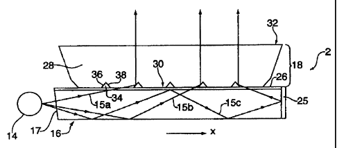
One preferred embodiment of the present invention is shown in Fig.
1. An illumination system 2 comprises a light generating means 14, a
waveguide 16 having a light accepting surface 17 and a transparent
reflecting means 18 in optical cooperation with waveguide 16. Optical
cooperation is meant to mean any relationship between waveguide 16 and
reflecting means 18 which enables light to pass from waveguide 16 to
reflecting means 18. Illustrative of useful light generating means 14 are
2 0 lasers, fluorescent tubes, light emitting diodes, incandescent lights,
sunlight and the like.
The reflecting means 18 comprises an optional low index of
refraction layer 26, which could also function as an adhesion promoting
layer, and an array of lenticular microprisms 28. The length of
microprisms 28 is aligned in the general direction of the travel of the light
through waveguide 16. Light reflects through waveguide 16 via total
internal reflection (TIR) in the general direction of the X axis and enters a
microprism 28 by way of light input surface 30 and exits the microprism 28
CA 02322326 2000-08-30
WO 99/45317 PCT/US99/04567
- 5 -
through the light output surface 32 as a spatially directed light source as
illustrated by exemplary light rays 15a-15c. Light input surface 30 is
further defined by selected surface voids 34 that, where present along the
light input surface, inhibit the transmission of light from the waveguide to
the reflecting means as illustrated by light ray 15c. Voids 34 can be
characterized as channels or grooves, defined by a material having a
refractive index less than the refractive index of waveguide 16 or refraction
layer 26, that interrupt the continuity of light input surface 30.
Referring also to Fig. 2, voids 34 are interstitial regions defined by
1o sidewalls 36 and 38 which further define the interface between the
refractive indices of microprism 28 and voids 34. Voids 34 may be of any
shape as long as the shape is tapered and the width of the "bottom" of the
void near the waveguide is wider than the width of the "tope of the void.
Surfaces 36 and 38 may be flat, curved, or faceted. For illustrative
purposes only, fig. 2 defines voids 34 as "V"-shaped grooves with flat
sidewalls 36 and 38. Voids 34 comprising sidewalls 36 and 38 extend
through microprism 28 in a direction generally perpendicular to the
direction of travel of light rays in the x axis. Preferably, voids 34 extend
the entire width of the microprism 28, but it is not necessary. In the case
2 o where sidewalls 36 and 38 are flat, they form angles 8 and 8',
respectively,
relative to the normal of input surface 30. Voids 34 prevent light from
entering microprism 28 as shown in Fig. 1 due to the differences in
refractive indices between waveguide 16 or the low index layer 26 and
void 34. The interstitial regions of void 34 must have an index of refraction
less than the index of refraction of the waveguide 16 or low index layer 26.
Preferred materials for void 34 include air, with an index of refraction of
1.00 and fluoropolymer materials with an index of refraction ranging from
about 1.16 to about 1.40. The most preferred material is air. In addition,
CA 02322326 2000-08-30
WO 99/45317 PCT/US99/04567
- 6 -
sidewalls 36 and 38 redirect a portion of light rays that enter microprism
28 through input surface 30.
Referring to Fig. 2, angles 8 and 8' do not have to be equal. Angles
8 and 8' control the direction of the light escaping from the microprisms
and are important for determining the degree of collimation of the output
light. These angles can vary over a wide range depending on the desired
output angle of the light and the desired degree of collimation. If a single
light source is used in an application as shown in Fig. 1, only the value of
angle 8 is important to redirect light. For the special case where sidewalls
36 and 38 are flat and where the desired output angle is perpendicular to
the plane of the waveguide , the desired values of angle 8 range from
about 15 degrees to about 50 degrees. More preferred values range from
about 20 degrees to about 40 degrees. The value of angle 8' is important
if light rays travel in both directions along the x axis. This is possible, if
for
example, reflective means 25 is applied to a surface of waveguide 16 (Fig.
1 ), opposite light accepting surface 17 or a second light source 14a is
utilized as shown in Fig. 4. Reflective means 25 may be a mirror,
reflective tape or any other highly reflective material.
Waveguide 16 may be any material that is transparent to light.
2 o Preferably waveguide 16 is transparent to light within the wavelength
range from about 400 to about 700 nm.. The preferred index of refraction
of the waveguide 16 is greater than about 1.30. More preferred indexes of
refraction may range from about 1.40 to about 1.65. Preferred materials
include transparent polymers, glass and fused silica. Desired
characteristics of these materials include mechanical and optical stability
at typical operation temperatures of the device. Most preferred materials
are glass, acrylic, polycarbonate and polyester. Alternatively, the
waveguide may be a cavity having a reflective surface with the exception
CA 02322326 2000-08-30
WO 99/45317 PCT/US99/04567
of the area that defines the light input surface. Cavity reflectance can be
achieved using aluminum coated smooth surfaces.
Microprisms 28 can be constructed from any transparent solid
material. Preferred materials have a refractive index between about 1.40
and about 1.65 and include polymethylmethacrylate, polycarbonate,
polyester, poly(4-methyl pentane), polystryrene, allyl diglycol carbonate,
polystyrene-co-acrylonitrile) polystyrene-co-methyl methacrylate),
silicone, polyurethanes and polymers formed by photopolymerization of
acrylate monomers.
Referring to Fig. 4, microprisms 28 are constructed to form a six-
sided geometrical shape having a light input surface 30, a light output
surface 32, wherein the light output surface 32 is larger in surface area
than the light input surface 30. Microprism 28 further comprises two pairs
of oppositely disposed sidewalls 46, 48 and 50, 52. Sidewalls 50 and 52
are effective in reflecting and redirecting the light which is propagating
through microprism 28. In most cases, sidewalls 46 and 48 have no
optical function. However, it may be necessary.to tilt sidewalls 46 and 48
so that light reflecting from voids 34 will not strike sidewalls 46 and 48.
Referring to Fig. 5, sidewalls 52 and 50 form a tilt angle ~ to the
2 o normal of the surface of waveguide 16. Sidewalls 52 and 50 help control
the output collimation in the direction parallel to input 17 of the light
transmitting means. The desired values of tilt angle ~ range from about 0
degrees to about 30 degrees. More preferred values for tilt angle ~ range
from about 5 degrees to about 20 degrees. Preferably, the tilt angles ~
associated with sidewalls 52 and 50 are equal, but equal angles are not
necessary.
The height 54 may vary widely depending on the dimensions and
resolution of the display or lighting application. That is, smaller displays,
CA 02322326 2000-08-30
WO 99/45317 PC'f/~3599/04567
_ g _
such as laptop computer displays and avionics displays would have
greatly reduced dimensions versus larger displays such as large screen,
flat-panel televisions.
Referring again to Fig. 1, the optional low index of refraction layer
26 is any material that is light transmissive and has an index of refraction
that is lower than the index of refraction of waveguide 16. The low index
of refraction layer may be either an inorganic material such as magnesium
fluoride or an organic material such as silicone. If layer 26 is also an
adhesion promoting Payer, it will cause the microprisms 28, especially
1 o microprisms formed from polymers, to adhere strongly to the waveguide
16. The thickness of the low index of refraction layer 26 is not critical and
can vary widely. In the preferred embodiment of the invention, low index
of refraction layer 26 is less than about 75 micrometers thick.
Referring again to Fig. 4 and as would be obvious to those skilled in
the art, microprisms 28 may have any repeat distance 40 in the y
direction. Further, the repeat distance 42 of voids 34 may vary in the x
direction. Distances 40 and 42 may vary depending on the resolution and
dimensions of an electronic display or the lumens output requirement of a
lighting application. Further, in the single light source application shown in
2 o Fig. 3a, distance 42 may vary widely across the surface of waveguide 16
in order to compensate for a lowering of the light intensity inside
waveguide 16 as the distance from light generating means 14 increases.
In this application, the repeat distance 42 would be smaller closer to the
light accepting surface 17 and gradually increase moving away from light
source 14. In essence, closely-spaced voids 34 decrease the amount of
light input surface area adjacent to light accepting surface 17 and widely-
spaced voids 34 increase the available light input surface area remote
from light accepting surface 17. Alternatively, light input surface may be
CA 02322326 2000-08-30
WO 99/45317 PCT/US99/04567
_ g _
varied across the microprism 28 by varying the depth 41 of interruption 34
as shown in Fig. 3b.
In an alternate embodiment, reflecting means 18 further comprises
a lenticular array of cylindrical microlenses 60 as shown in Fig. 6.
Alternatively, the lenticular microlens curvature may have a shape other
than cylindrical, such as, and for example only, an elliptical or a parabolic
cross section. The microlenses 60 are disposed in close proximity to the
microprisms 28. The microlenses 60 preferably have a index of refraction
equal to the index of refraction of the microprisms 28. However,
1 o microlenses 60 could be fabricated in a separate process from the
microprisms 28 and any transparent material may be used, as for
example, those materials previously discussed. If a separate process is
used to fabricate the microlenses 60, it is preferred that the index of
refraction of the microlenses 60 be equal or substantially equal to the
index of refraction of the microprisms 28. The center-to-center distance
between microlenses directly correlates to the repeat distances 40 of the
microprisms 28. That is, for every microprism 28 there exists a
corresponding microlens 60 that aligns with the output surface 32 of each
microprism 28.
2 o A spacer 62 separates the microlenses 60 and the microprisms 28.
The thickness of spacer 62 is optimized~to cause light from microprisms
28 to be collimated by microlenses fi0. Preferably spacer 62 is molded in
the same process that was used to mold microprisms 28 and microlenses
60 and therefore is the same material as the microprisms 28 and
microlenses 60. However, in general, spacer 62 may be fabricated
separately from any transparent material. Preferred materials include
transparent polymers, glass and fused silica. Preferably spacer 62 has an
index of refraction equal to or substantially equal to the index of refraction
CA 02322326 2000-08-30
WO 99/45317 PCTNS99/04567
- 10 -
of the microprisms 28 and the microlenses 60. Desired characteristics of
these materials include mechanical and optical stability at typical operation
temperatures of the device. Most preferred materials are glass, acrylic,
polycarbonate and polyester.
Arrays of microprisms 28 separately or in combination with
microlenses 60 can be manufactured by any number of well known
techniques such as molding, including injection and compression molding,
casting, including hot roller pressing casting, photopolymerization within a
mold and photopolymerization processes which do not employ a mold.
1 o One advantage of the invention over the prior art is the lenticular
arrangement which facilitates the fabrication process by facilitating the
free flow of resin within a mold. A preferred manufacturing technique
would be one that allows the reflecting means 18 which comprises an
array of microprisms 28, an array of microlenses 60 and a spacer 62 to be
manufactured as a single integrated unit. An advantage of this technique
would be the elimination of alignment errors between the array of
microprisms and microlenses if the arrays were manufactured separately
and then attached in the relationship described above. Preferably
reflecting means 18 is manufactured by injection or compression molding.
2 o Example
A polystyrene part was injection molded having lenticular prisms in
combination with cylindrical lenses as shown in Fig. 6. The lenticular
prisms ware 0.0125 inches wide at the base of the prism and 0.020 inches
wide at the top of the prism. The prisms had a height of 0.019 inches.
The cylindrical lenses were separated from the tops of the prisms by a
polystyrene spacer layer 0.025 inches thick. There was one cylindrical
lens for each lenticular prism. The cylindrical lenses had a radius of
curvature of 0.024 inches and were aligned with the tops of the prisms.
CA 02322326 2000-08-30
WO 99/45317 PCT/US99/04567
- 11 -
The lenticular prisms had "V-shaped" grooves or voids positioned every
0.016 inches along the long direction of the prisms. The depth of the
grooves was 0.0097 inches.
The polystyrene part was attached to a clear acrylic waveguide
using a silicone pressure-sensitive adhesive layer 0.001 inches thick. The
silicone pressure-sensitive adhesive had a refractive index of 1.41, which
was lower than the refractive index of both the acrylic waveguide
(refractive index = 1.49) and the polystyrene molded part (refractive index
= 1.59). Light from two fluorescent lamps was coupled into two opposing
to ends of the acrylic waveguide. The general direction of the light was
parallel to the direction of the lenticular prisms and lenses of the attached
molded part. Light in the waveguide was able to pass through the silicone
layer and enter the molded part in the regions where the molded part
touched the pressure-sensitive adhesive. The surface area on the
waveguide occupied by the voids (refractive index = 1.00) did not allow
light to pass from the waveguide. The walls of the void redirected light
within the lenticular prisms. The light emerged from the molded part
highly collimated and in a direction approXimately perpendicular to the
plane of the waveguide. The light had collimation angles (the full width of
2o the peak at the half maximum points) of ~ 14 ° in one direction and
t 13.7
° in the perpendicular direction. Cross-sectional views of the light
distribution in two perpendicular directions are shown in Figure 7.
It will be understood that the particular embodiments described
above are only illustrative of the principles of the present invention, and
that various modifications could be made by those skilled in the art without
departing from the scope and spirit of the present invention, which is
limited only by the claims that follow.