Note: Descriptions are shown in the official language in which they were submitted.
CA 02322363 2000-10-OS
1
METHOD OF FORMING CHROMIUM COATED COPPER FOR PRINTED
CIRCUIT BOARDS
Field of the Invention
This invention relates to a process for treating copper and, more
particularly, to
a process for applying a metal to at least one side of a copper foil.
Background of the Invention
Copper foil is used in the production of printed circuit boards. In the
production of printed circuit boards, it is generally necessary to bond a
copper foil to a
dielectric substrate to provide the foil with dimensional and structural
stability.
Although an excellent electronic conductor, there are problems inherent with
the use
of copper foil. For example, copper is easily oxidized and corroded, and
copper itself,
whether plated or rolled, does not adhere well to such substrates. Copper is
also
known to accelerate or catalyze the decomposition of the dielectric
substrates. For
these reasons, copper foil is typically sold with one or more protective
layers applied
to its surface.
It is known that a thin, chromium layer deposited onto copper foil has many
applications for printed circuit boards. There are two ways to deposit the
thin
chromium layer onto a copper surface. One is by an electrodeposition process,
and the
other is by a vacuum deposition process.
The electrodeposition process has several disadvantages. Foremost, the
process uses environmentally hazardous material that is difficult and costly
to handle
and dispose of. Further, this type of process is inexact and inefficient.
With respect to the vacuum deposition process, in order to insure a
satisfactory
adhesion between the applied chromium and copper, an extensive and rigorous
pre-
treatment of the copper is required to remove copper oxide from the surface
thereof
prior to the vacuum deposition of the chromium.
The present invention overcomes these and other problems and provides a
method of forming a metal coated copper by a vacuum deposition process that
does
not require an extensive rigorous pre-treatment process.
Summary of the Invention
In accordance with a preferred embodiment of the present invention, there is
provided a method of applying a metal onto a copper layer, comprising the
steps of
stabilizing a surface of a copper layer by applying a stabilization layer
thereto, the
CA 02322363 2000-10-OS
2
stabilization layer comprised of zinc oxide, chromium oxide, nickel oxide or a
combination thereof and having a thickness of between about 5~ and about 70~,
and
vapor depositing a metal selected from the group consisting of aluminum,
nickel,
chromium, copper, iron, indium, zinc, tantalum, tin, vanadium, tungsten,
zirconium,
molybdenum and alloys thereof onto the stabilized surface of the copper layer.
One
specific alloy contemplated herein is nickel-chromium alloy.
In accordance with another aspect of the present invention, there is provided
a
sheet material comprised of a layer of copper and a stabilization layer on a
surface of
the copper. The stabilization layer is comprised of zinc oxide, chromium
oxide, nickel
oxide or a combination thereof and has a thickness between about 51~ and about
70A.
A vapor deposited metal is provided on the stabilized layer.
It is an object of the present invention to provide a chromium coated copper
layer for use in manufacturing printed circuit boards.
Another object of the present invention is to provide a method of forming a
chromium coated copper layer as described above by a vacuum deposition process
that
does not require an extensive, rigorous pre-cleaning of the copper surface
prior to
deposition of the chromium.
Another object of the present invention is to provide a method of vacuum
depositing a metal onto a copper surface.
A still further object of the present invention is to provide a generally
continuous process as described above.
These and other objects will become apparent from the following description
of a preferred embodiment taken together with the accompanying drawings and
the
appended claims.
Brief Description of the Drawings
The invention may take physical form in certain parts and arrangement of
parts, a preferred embodiment of which will be described in detail in the
specification
and illustrated in the accompanying drawings which form a part hereof, and
wherein:
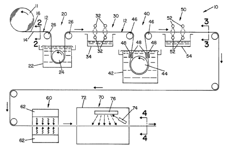
FIG. I is a schematic view of a process for applying a metal onto a surface of
a
copper foil in accordance with the present invention;
FIG. 2 is an enlarged sectional view taken along lines 2-2 of FIG. 1 showing a
sheet of copper foil;
CA 02322363 2000-10-OS
3
FIG. 3 is an enlarged sectional view taken along lines 3-3 of FIG. 1 showing
the sheet of copper foil of FIG. 2 with stabilization layers thereon; and
FIG. 4 is an enlarged sectional view taken along lines 4-4 of FIG. 1 showing a
sheet of copper having a vapor deposited metal on the matte side thereof.
Detailed Description of Preferred Embodiment
The present invention relates to a process for applying a metal onto a copper
surface. As used herein the term "metal" refers to metals and alloys capable
of
vacuum deposition by the methods disclosed herein. The invention is
particularly
applicable to applying chromium onto copper foil and will be described with
particular
reference thereto, it being appreciated however, that the disclosed process
may also be
used in applying a metal such as aluminum, nickel, copper, iron, indium, zinc,
tantalum, tin, vanadium, tungsten, zirconium, molybdenum and alloys thereof
onto
copper foil.
The copper foils used with this invention can be made using one of two
1 S techniques. Wrought or rolled copper foil is produced by mechanically
reducing the
thickness of a copper or copper alloy strip or ingot by a process such as
rolling.
Electrodeposited foil is produced by electrolytically depositing copper ions
on a
rotating cathode drum and then peeling the deposited foil from the cathode.
Electrodeposited copper foils find advantageous application with this
invention.
The copper foils typically have nominal thicknesses ranging from about 0.0002
inch to about 0.02 inch. Copper foil thickness is sometimes expressed in terms
of
weight and typically the foils of the present invention have weights or
thicknesses
ranging from about '/g to about 14 ounces per square foot (oz/ftz). Especially
useful
copper foils are those having weights of '/3, %z, 1 or 2 oz/ft2.
Electrodeposited copper foils have a smooth or shiny (drum) side and a rough
or matte (copper deposit growth front) side. The stabilization layer applied
by the
inventive process can be applied to either side of the foil, and in some
instances it is
applied to both sides. In one embodiment, the layer applied by the inventive
process is
applied to the shiny side of the foil.
The side or sides of the foil, to which the layer applied by the inventive
process
overlies, can be a "standard-profile surface," low-profile surface" or "very-
low-profile
surface." Useful embodiments involve the use of foils with low-profile
surfaces and
very low-profile surfaces. The term "standard-profile surface" is used herein
to refer
CA 02322363 2003-12-04
4
to a foil surface having an Rtm (IPC-MF-150F) of greater than 10.2 microns.
The teen
"low-profile surface" refers to a foil surface having an R"" (IPC-MF-150F} of
less than
10.2p. The term "very-low-profile surface" refers to a foil surface having an
R,",
(IPC-MF-150F) of less than S.lp. R~," (IPC-MF-150F) is the mean of the maximum
peak-to-valley vertical measurements from each of five consecutive sampling
measurements, and can be measured using a SURTR~NIC~ 3 profilometer marketed
by Rank Taylor Hobson, Ltd., Leicester, England.
It will be appreciated by those skilled in the art that the present invention
not
only applies to copper foil having a stabilization layer on a surface thereof,
but also
applies to copper layers that have been deposited or adhered to other
substrates and
that have a stabilization layer applied on a surface thereof, after deposition
or before or
after being adhered to another substrate. Such substrates include, but are not
limited
to, polyimide (see U.S. Patent Nos. 5,685,970 and 5,681,443 , other polymeric
substrates, organic substrates, aluminum (see U. S. Patent No. 5,153,050),
metal
substrates (see U.S. Patent No. 5,674,596) or laminates of copper and INVAR.
Referring now to the drawings wherein the showings are for the purpose of
illustrating the preferred embodiment of the invention only, and not for the
purpose of
limiting same, FIG. 1 is a schematic view of a generally continuous
manufacturing
process 10 for applying a metal onto a copper surface illustrating a preferred
embodiment of the present invention. In the embodiment shown, a roll 11
provides a
generally continuous strip of copper foil 12. FIG. 2 is an enlarged cross-
sectional
view of copper foil 12. The copper foil 12 has a shiny side 14 and a matte
side 16. (In
the drawings, matte side 16 of copper foil 12 is shown exaggerated for the
propose of
illustration).
Copper foil 12 preferably undergoes a first cleaning process, designated 20 in
the drawings, to remove oxide film on the surfaces thereof. In the embodiment
shown,
copper foil 12 is conveyed into a tank 22 around a guide roll 24 by means of
guide
rollers 26. Tank 22 contains a cleaning solution to remove oxide film from the
surfaces of copper foil 12. An acid solution is preferably used to remove the
copper
oxide layer from copper foil 12. A typical acid solution for cleaning copper
foil 12
CA 02322363 2003-12-04
may include 10-80 g/1 HZS04. In one embodiment, 50 g/1 HzS04 is used to remove
the copper oxide layer from copper foil 12.
After cleaning process 20, copper foil 12 undergoes a rinsing process,
designated 30, wherein spray elements 32 disposed above and below copper foil
12
5 spray the surfaces of copper foil 12 with water. A tank 34 disposed beneath
spray
elements 32 collects the water sprayed therefrom.
Following cleaning process 20 and rinsing process 30, copper foil 12
undergoes a stabilization process, designated 40. Copper foil 12 is directed
into a tank
42 and around a guide roll 44. Copper foil 12 is positioned relative to guide
roll 44 by
guide rollers 46. Tank 42 contains an electrolytic solution. In accordance
with one
embodiment of the present invention, the electrolytic solution contains zinc
ions and
chromium ions. The source of zinc ions for the electrolytic solution can be
any zinc
salt, examples include ZnS04, ZnC03, ZnCr04, etc. The source of chromium ions
for
the electrolytic solution can be any hexavalent chromium salt or compound,
examples
include ZnCr04, Cr03, etc.
The concentration of zinc ions in the electrolytic solution is generally in
the
range of about 0.1 to about 2 g/l, preferably about 0.3 to about 0.6 g/1, and
more
preferably about 0.4 to about 0.5 g/1. The concentration of chromium ions in
the
electrolytic solution is generally in the range of about 0.3 to about 5 g/1,
preferably
about 0.5 to about 3 g/1, and more preferably about 0.5 to about 1.0 g/l.
In another embodiment, nickel oxide or nickel metal may also be deposited by
itself or co-deposited with either zinc oxide or chromium oxide or both to
form the
stabilization layer. The source of nickel ions for the electrolytic solution
can be any of
the following individually or in combination: Ni2S04, NiC03 etc.
The concentration of nickel ions in the electrolytic solution is generally in
the
range of about 0.2 g/1 to about 1.2 g/l.
In another embodiment, other stabilization layers such as those containing
phosphorous as is disclosed in U.S. Patent No. 5,908,544, may be used.
The electrolytic solution can include other conventional additives such as
Na2S04 at concentrations in the range of about 1 to about 50 g/l, preferably
about 10
to about 20 g/1 and more preferably about 12 to about 18 g/1. The pH of the
CA 02322363 2000-10-OS
6
electrolytic solution is generally in the range of about 3 to about 6,
preferably about 4
to about 5, and more preferably about 4.8 to 5Ø
The temperature of the electrolytic solution is generally in the range of
about
20°C. to about 100°C., preferably about 25°C. to about
45°C., and more preferably
from about 26°C. to about 44°C.
As seen in FIG. 1, anodes 48 are disposed adjacent to each side of copper foil
12 to apply a current density to copper foil 12. Guide rollers 46 are cathodic
rollers
wherein a stabilization layer 49 comprised of zinc oxide and chromium oxide is
deposited on the exposed shiny side 14 and matte side 16 of copper foil 12
when
anodes 48 are energized by a power source (not shown). FIG. 3 is a cross-
sectional
view showing copper foil 12 with stabilization layers 49 on shiny side 14 and
matte
side 16.
The current density is generally in the range of about 1 to about 100
amps/ft2,
preferably about 25 to about 50 amps/ft2, and more preferably about 30
amps/ftz.
Where multiple anodes are employed, the current density may be varied between
the
anodes.
The plating time that is used is generally in the range of about 1 to about 30
seconds, preferably about 5 to about 20 seconds, and more preferably about 15
seconds. In one embodiment, the total treatment time on the shiny or smooth
side is
from about 3 to 10 seconds, and on the matte side is from about 1 to about 5
seconds.
In one embodiment, the mole ratio of chromium ions to zinc ions in the
electrolytic solution is in the range of about 0.2 to about 10, preferably
about 1 to
about 5, and more preferably about 1.4.
In accordance with the present invention, the thickness of stabilization
layers
49 that are applied to copper foil 12 are between about 5~ to about 70A, and
preferably about 20th to about SOt~.
In the embodiment heretofore described, stabilization layer 49 is comprised of
chromium oxide and zinc oxide. In accordance with another aspect of the
present
invention, stabilization layer 49 is comprised of only chromium oxide. The
bath
chemistries and process conditions for applying a chromium oxide stabilization
layer
are as follows:
1 - 10 g/1 Cr03 solution
Preferred 5 g/1 CT03
CA 02322363 2000-10-OS
7
pH-2
Bath temperature: 25°C
- 30 amps/ft2 for 5 - 10 seconds
or dip treatment: 10 seconds
5 Following stabilization process 40, copper foil 12 with stabilization layers
49
thereon then undergoes a rinse process, designated SO in the drawings. Spray
elements
52, disposed above and below copper foil 12, spray water onto the surfaces of
copper
foil 12 (with stabilization layers 49) to rinse and clean the same and to
remove any
residual electrolytic solution therefrom. A tank 54 disposed below spray
nozzles 52
10 collects the rinsing solution.
Copper foil 12 with stabilization layers 49 thereon undergoes a drying process
60 schematically shown in FIG. 1. In the embodiment shown, forced air dryers
62 are
disposed above and below copper foil 12 to direct air onto copper foil 12 to
dry the
surface thereof.
In accordance with the present invention, following application of
stabilization
layers 49, a metal is vacuum deposited onto one or both stabilized surfaces of
copper
foil 12. In the embodiment shown in FIG. 1, the metal is applied to matte side
16 of
copper foil 12. The metal may be any metal capable of vacuum deposition
including
those selected from the group consisting of aluminum, nickel, chromium,
copper, iron,
indium, zinc, tantalum, tin, vanadium, tungsten, zirconium, molybdenum and
alloys
thereof. In accordance with the present invention, the metal is vacuum
deposited onto
the stabilization layer 49 on copper foil 12 without additional cleaning or
surface
preparation. The metal is applied directly onto stabilization layer 49 by
vacuum
deposition techniques such as sputtering, chemical vapor deposition, electron
beam
deposition, thermal evaporation, ion plating (via substrate) or a combination
of such
processes. In the embodiment shown, a sputtering process 70 is schematically
illustrated. As seen in FIG. l, copper foil 12 with stabilization layers 49
thereon is
conveyed into a deposition chamber designated 72. An electron beam gun 74
directs a
stream of electrons at a target 76 comprised of a metal such that metallic
species are
knocked loose and deposited onto a surface of copper foil 12. In the
embodiment
shown, the deposition process applies a metal onto the matte side of copper
foil 12.
The applied metal preferably has a thickness of between about SOA and S,OOOA.
In
CA 02322363 2000-10-OS
8
the embodiment shown, a single target 76 is illustrated. As will be
appreciated,
multiple targets may be used and, if desired, the metal may be applied to both
matte
side 16 and shiny side 14 of foil 12.
In a preferred embodiment of the present invention, chromium is sputter
deposited onto matte side 16 of copper foil 12 as an adhesion layer to enhance
the
adhesion of the copper foil to a substrate. It has been found that the
foregoing process
provides a chromium coated copper foil having good adhesive properties.
The following examples are provided for purposes of illustrating the
invention.
Unless otherwise indicated, in the following example as well as throughout the
specification and claims, all parts and percentages are by weight, all
temperatures are
in degrees Celsius, and all pressures are atmospheric.
EXAMPLE 1
Both sides of raw electrodeposited copper foil '/s oz/ft2, are pretreated with
1 S stabilization layers as follows:
Stabilization Treatment:
0.53 gll Zinc as ZnS04 ,0.6 g/1 Cr as Cr03, 11 g/1 Na2S04
Bath pH: 5.0
Bath temperature: 42°C.
Current density: 8-15 amps/ftz for matte side
2-2.5 amps/ft2 for shiny side
Plating time: shiny side: 6-8 seconds
matte side: 3-4 seconds
Chromium is then applied to the stabilization layers) as follows:
Chromium Sputtering:
14" sputter machine
Power: 5-8 kilowatts
Linear speed: 1.4 to 2.2 ftlmin
Chromium Thickness: 1,200A for matte side
1,300A for shiny side
CA 02322363 2000-10-OS
9
EXAMPLE 2
Both sides of polyimide film are plated with copper (18~ copper/50u
polyimide film/Sp copper; this product is one of a family of Gould~flex
products
manufactured by Gould Electronics Inc.) and treated as follows:
S Stabilization Treatment:
0.53 g/l Zinc as ZnS04, 0.6 g/1 Cr as Cr03, 11 g/1 NazS04
Bath pH: 5.0
Bath temperature: 42°C.
Current density: 25 amps/ft2 for both sides
Plating time: for either or both sides: 3-8 seconds
Chromium is then applied to the stabilization layers) as follows:
Chromium Sputtering:
14" sputter machine
Power: 5-8 kilowatts
Linear speed: 1.8 to 2.8 ft/min
Chromium Thickness: 1,OOOt~ for 18p copper side
No chromium applied to Sp copper side
EXAMPLE 3
Both sides of polyimide film are plated with copper (18p copper/SOp
polyimide film/5~, copper; this product is one of a family of Gould~flex
products
manufactured by Gould Electronics Inc.) and treated as follows:
Stabilization Treatment:
5 g/1 Cr as Cr03
Bath pH: 2.0
Bath temperature: 25°C.
Dip treatment
Chromium is then applied to the stabilization layers) as follows:
Chromium Sputtering:
14" sputter machine
Power: 5-8 kilowatts
Linear speed: 1.8 to 2.8 ft/min
Chromium Thickness: 1,000 for 18p copper side
CA 02322363 2000-10-OS
EXAMPLE 4
Both sides of electroplated 8p, copper on INVAR (8p Cul 1.5 mil INVAR/8p
Cu), are pretreated with stabilization layers as follows:
Stabilization Treatment:
5 0.53 g/1 Zinc as ZnS04, 0.6 g/1 Cr as Cr03, 11 gll Na2S04
Bath pH: 5.0
Bath temperature: 42°C.
Current density: 25 amps/ft2
Plating time: 3-4 seconds
10 Chromium is then applied to the stabilization layers) as follows:
Chromium Sputtering:
14" sputter machine
Power: 5-$ kilowatts
Linear speed: 1.8 to 2.8 ftlmin
Chromium Thickness: 1,000 for 8p copper side
The foregoing description is a specific embodiment of the present invention.
It
should be appreciated that this embodiment is described for purposes of
illustration
only, and that numerous alterations and modifications may be practiced by
those
skilled in the art without departing from the spirit and scope of the
invention. For
example, cleaning process 20 may not be required if process 10 is an extension
of an
electroforming process wherein virgin copper is being formed and directed into
process line 10. Further, while the foregoing process has been described with
respect
to a copper foil, the process may be used to apply a metal, such as chromium,
onto
copper that is part of a copper coated polymer. It is intended that all such
modifications and alterations be included insofar as they come within the
scope of the
invention as claimed or the equivalents thereof.