Note: Descriptions are shown in the official language in which they were submitted.
CA 02322459 2000-09-07
WO 98/49652 1 PCT/SE98/00798
Smartcard and method for- its manufacture
Introduction
The present invention relates to a smartcard, particularly a smartcard with an
integrated LCD display unit and browse buttons, that fulfils the criteria of
ISO 7816
and a method for the manufacture of such a smartcard. The present invention
also
relates to an apparatus for performing the manufacturing procedure.
Smart cards are small electronic devices comprising a processor and an
electronic
data memory, the contents of which may be modified throu'h the processor by an
external card accessing device. The processor provides processing capabilities
which can include encryption of stored data, identification functions and the
like.
They are increasingly used in place of more traditional transaction cards
(e.g. credit
or identification cards) in which data are recorded on a magnetic strip. Smart
cards
have a larger storage capacity than magnetic srizp cards which do not have a
processor and therefore cannot process stored information.
Recently so-called general purpose smart cards have been disclosed which have
a
display and a user control means such as a keypad. They have the advantage,
compared with the ordinary smart cards, that they do not need specific
terminal
equipment for referencing their contents and inputting data. These smartcards
can
be used in many different everyday situations in areas such as, for example,
payment, service, health care, transport (as a voucher or a ticket),
communication,
identification and multipurpose.
In order to standardise smartcards an ISO standard, ISO 7816. has been drawn
up
for them. The standard ISO 7816 has 3 different parts:
- ISO 7816-1 which defines the physical characteristics of the card.
CONFIRMATION
COPY
CA 02322459 2000-09-07
WO 98/49652 ~ PCT/SE98/00798
- ISO 7816-2 which defines dimension and contact position of the card.
- ISO 7816-3 which defines the electrical signals and ri-ansmission protocols.
While it is relatively easy to arrange the contact positions and the
electrical signals
and protocols, it has previously been impossible to fulfil all the physical
requirements of ISO 7816-1 and -2 for a smart card having a display and user
control means. These requirements include that:
the surface profile of card and contacts should be such that the difference in
level
between all contacts and the adjacent card surface shall be less than 0.1 mm;
the mechanical strength of the card and contacts should be such that the card
shall
resist damage to its surface and any components contained in it and shall
remain
intact during normal use, storage and handling,
the surface, and contact pins, must not be damaged by the pressure caused by a
steel
ball of 1.5 mm diameter on which is applied a force of l.~ N,
the electrical resistance measured between any two points of the contact pins
must
not be over 0.5 Ohm, with a cuiTent of from 50 ~A to 300 mA;
the short ends of the card should be able to be flexed through a deformation
of 2 cm
measured from the centre of the card, at a rate of 30 bend per minute for 1000
bends
without any cracks forming and without the card malfunctioning,
the long sides of the card should be able to be flexed tlu~ough a deformation
of 1 cm
measured from the centre of the card, at a rate of 30 bend per minute for 1000
bends
without any cracks forming and without the card malfunctioning;
the card must be not more than 0.76 mm thick.
Thus the card must be strong, thin and flexible. In this context, flexible is
defined as
being able to fulfil the ISO 7816 requirements for flexibility as well as all
the other
ISO requirements. A card which fulfils all the requirements of ISO 7816 and
which
has a display and user control means will henceforth be called a super smart
card.
Cards containing processors but not fulfilling the requirements of ISO 7816 or
lacking a display will be called general purpose cards, chip cards or smart
cards.
CA 02322459 2000-09-07
WO 98/49652 ~ PCT/SE98/00798
Chipcards with displays and keypads are known from, for example, EP, A , 405
054, FR, A, 2731 X37, JP, A, 7329462, WO, A, 9420929, US X521362 and "Low-
power one-chip microcomputer with 64 Kbit EEPROM for smart card." Yaegawa,
K.; Eby, M.D.; Kobayashi, M.; Takeuchi, W. Sharp Technical Journal (Dec. 1991)
no. 51, p.67-72. These cards also contain an internal power source. These
cards are
too thick and/or stiff to conform with the ISO 7816.
A prior art method for the manufacture of chip cards is disclosed in "New
packaging
technology of super smart card" ,Watahiki, S.; Ohta, S.; Murakami, A.; Inaba,
T.;
Takahashi, H. (Oki Electr. and. Co. Ltd., Japan) Sixth IEEEICHMT International
Electronic Manufacturing Technology, Symposium. Proceedings 1989 Japan IEMT
Symposium (Cat. No.89CH2741-7), New York, NY, USA: IEEE, 1989. p.101-4,
Conference: Nara, Japan, 26-28 April 1989. In this method the processor
("chip"),
which has 92 pins and a surface area of nearly ~0 square mm, is mounted on a
first
printed circuit board, called a terminal board, by an outer lead bonding
method. In
this method each of the 92 pins on the chip is connected to different one of
92 leads
on a circuit board surrounding the chip. This terminal board is then aligned
with a
second painted circuit board and connected to it by anisoti~opic adhesive.
This
second board is then joined together with a back film layer, a back panel, an
adhesive film, a plurality of frame films, a hot melt film, a front panel and
a front
film to form a card. A problem with this method is that the anisotropic
adhesive
used is brittle and therefore can break if the card is flexed. The adhesive is
formed
of 301,un diameter cores of low melting-point solder spaced at 80~m centres.
This
limits its use to connecting components which are spaced at least ~O~m apart
and
hence it is not suitable for the cun-ent generation of microprocessors which
have
only 20~rn between pins. A further limitation with this method is that the
large size
of the chip means that it would be easily damaged if the card was sufficiently
flexible to fulfil the ISO 7816 requirements. To avoid these problems the
cards have
to be made stiff i.e. they have limited flexibility and cannot fully conform
with the
ISO 7816 standard.
CA 02322459 2000-09-07
WO 98/49652 ~ PCT/SE98/00798
Thus no card with a display has been disclosed in the prior art which can
fulfil all
the requirements of ISO 7816 regarding strength and flexibility while also
fulfilling
the dimensional limitations, particularly in thickness, imposed by said
standard.
An object of the present invention is to produce a thin, flexible and sn~ong
super
smartcard (i.e. a card with a processor, display and user control means) which
can
work properly and withstand, without cracking or malfunctioning, the stress of
everyday situations which include, for example, bending of the card and
subjecting
it to pressure.
A further object of the present invention is to provide a method for
manufacturing
such super smart cards.
Another object of the invention is to provide an apparatus suitable for
manufacturing such super smart cards.
Summary of the invention
The present invention solves the problem of how to provide a smancard with a
display and user control means such as browse buttons or a keypad, which is
thin,
strong and flexible. This is achieved by building a smart card of a number of
thin
layers of materials with specially selected physical properties and combining
these
layers with specially adapted, flexible assembly techniques.
The super smartcard manufactured in accordance with the present invention can
conform to the ISO 7816 standard.
The invention will be described in more detail below with reference to
examples of
embodiments as shown in the appended drawings.
Brief description of the drawings
CA 02322459 2000-09-07
WO 98/49652 j PCT/SE98/00798
Figure 1 shows schematically an exploded view of one embodiment of a smart
card
according to the invention;
Figure 2 shows schematically an exploded view of a second embodiment of a
smart
card according to the invention;
Figure 3 shows schematically an apparatus for manufactwing a smart card
according to the first embodiment of the invention;
Figure 4 shows schematically an apparatus for manufacturing a smart card
according to the second embodiment of the invention.
Figures Sa) to ~I) show different embodiments of smart cards according to the
invention.
Detailed description of Embodiments
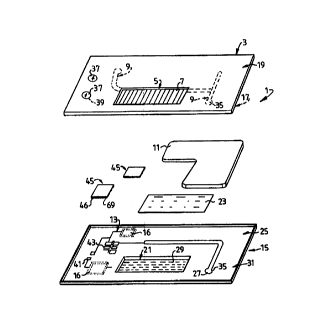
As shown in figure 1 an example of an embodiment for a smart card 1, e.g. of
super
smart card type, is made up of a number of carrier layers of different
materials. An
outer carrier layer 3, which is here called the top layer 3 for the sake of
clarity but
which could be the bottom layer depending on the oaientation of the smartcard
1, is
made of a flexible, resilient, can~ier material. Preferably the can-ier
material is a
polyester such as PET which suitable for flexible designs and as carrier for
ITO
(indium tin oxide-a transparent conductive agent which makes LCD displays
possible) and conductive circuits. While PET is cheap and readily available,
it is not
suitable for soldering as it cannot withstand any temperature higher than
about 100°
C. Top layer 3 has a window for a display ~ foamed in it by leaving a portion
of
PET transparent and the rest of the top layer 3 is preferably made opaque or
coloured or decorated by printing for aesthetic reasons. ITO 7 for the columns
of the
display, and conductive circuit tracks 9, made from copper, silver or anv
other
CA 02322459 2000-09-07
WO 98/49652 ~ PCT/SE98/00798
suitable conductive material, for the additional circuitry connecting a power
supply
11 to a main circuitry 13 on a bottom layer 15, are deposited onto the
underside 17
of the top layer 3. If made of copper then the tracks 9 are preferably 10-30
pm thick.
The upper side 19 of the top layer can be decorated as required.
In this embodiment a bottom layer 1~ is made of flexible, resilient, heat-
resistant
carrier material which is suitable for flexible designs and as Garner for ITO
and
conductive circuits. An example of such a material is the polymer PEN such as
the
type known as GTS 5660 from GTS Flexible Materials Ltd, United Kingdom. PEN
has a melting-point temperature of over 180° C which, as this is above
the melting-
point of about 160° C for low melting point solder, allows the
soldering and
FlipChip bonding of components attached to it. By FlipChip bonding is meant a
process where a chip is aligned with contacts on a surface, then placed with
its
solder coated pins in contact with the surface and bonded directly to the
surface by
soldering. PEN is furthermore suitable for use with other assembly methods
that can
be used with polymers. Other conceivable materials that could be used instead
of
PEN are epoxy or epoxy derivatives and also other polymers with similar
characteristics to PEN and which can attach to conducting tracks. A cavity 21
for
LCD fluid 23 is prepared, for example by embossing, in the upper side 25 of
bottom
layer 15 in a position corresponding to the position of display window 5 in
the top
layer. The cavity 21 is also preferably tt~ansparent in order to allow the
display ~ to
be read from either side of the card 1. Conductive tracks 27, made from
copper,
silver or any other suitable conductive material and preferably 10-30 wm thick
in the
case that they are made from copper, which form the main circuitry 13 of the
smart
card and ITO 29 for the rows of the display ~ are deposited on the upper side
2~ of
bottom layer 15. The cavity 21 is filled with LCD fluid 23 which in the
assembled
smart card 1 is in contact with the ITO columns 7 and rows 29 of the display
~. In
order for the LCD 5 to function it must have polarising display windows and in
the
embodiment of the invention shown the PET and PEN materials are polarising. It
is
also possible to use non-polarising PET and/or PEN in which case a translucent
polarising film would have to be applied to the window in the non-polarising
CA 02322459 2000-09-07
WO 98/49652 ~ PCT/SE98/00798
material. Thus in this embodiment an LCD display 5 is constzucted of 5-7
different
layers:
top plastic carrier (top, at least partly transparent, PET layer 3 );
translucent polarising film e.g. l OSwm thick (not shown and not required if
top layer
3 is polarising);
ITO columns 7 (for example, 5 columns per character);
LCD fluid 23 in cavity 21;
ITO rows 29 (for example, 7 rows per character);
translucent polarising film e.g. 175~m thick (not shown and not required if
bottom
layer 15 is polarising);
Bottom plastic carrier (bottom, at least partly transparent, PEN layer 15).
In order to comply with ISO 7816 the total thickness of this display 5 must be
equal
to 0.76 mm (plus or minus the tolerances given in ISO 7816).
The power source 11, preferably in the foam of a flexible, polymer-based (e.g.
polymer-lithium) laminar battery of any desired shape, is mounted in between
the
top and bottom layers 3 resp. 15 at any desired location. The conductive
circuitry 9,
13 on both top and bottom layers, by means of suitable plating, e.g. silver,
aluminium or tin, fomn contacts 35 for the power source 11 .
User control means, shown in this embodiment as a pair of browse buttons 37
made
of domes formed in the top layer 5, are provided. These domes can be coated
with
carbon 39 and are positioned over corresponding contact pad areas 41 provided
with
a suitable number of poles (not shown) in the copper circuit 13 in the bottom
layer
15. Any other suitable input means can also conceivably be used.
The card 1 is preferably provided with smaucard contacts 43, for erample in
the
form of gold plated areas 43 in the bottom copper circuitry 13, in accordance
with
the ISO 7816 minimum requirements.
CA 02322459 2000-09-07
WO 98/49652 g PCT/SE98/00798
One or more microprocessors, shown here as microchips 45, according to the
application for the card 1 (here two chips are shown), are integrated into the
space
between the top and bottom layers 3, 15. In this embodiment of the invention
the
pins 46 of the two chips 45 are attached to the underlying contacts 16 on the
bottom
layer 15 by flexible, conducting attachment means in the foam low melting-
point
temperature solder 69 which melts at a temperature below the melting point of
PEN.
Figure 2 shows a second embodiment of a super smantcard according to the
invention in which the same reference numbers as used here as in figure 1 to
refer to
similar items. In this embodiment the chips 45 are attached to the underlying
contacts by flexible, conducting attachment means in the form of a flexible
anisoti-opic adhesive 66.
In figure 3 an embodiment of an apparatus 50 for assembling a card according
to the
invention for manufacturing a card 1 is shown. Apparatus 50 comprises a
surface
mount machine 52 which is supplied with the pre-formed components which a.re
comprised in a card l and automatically assembles them into complete cards.
The
apparatus has pairs of feed and take-up reels 54, 56, 58 which supply bands of
material to the base assembly board 60.
The pair of reels 54 contain a band of polarising PET 55 which has been pre-
processed, in ways known in the art and thus not described here, so that, on
the
underside 17 facing the base assembly board 60, ITO patterns 7, copper tracks
9 and
browse buttons 37 have been foiined.
The pair of reels 56 contain a pre-cut band of laminating adhesive 57 which is
used
to adhesive the top and bottom layers 3, 15 together.
The pair of reels 58 contain a band 59 of polarising PEN which has been pre-
processed in ways known in the aut and thus not described here, so that on the
upper
CA 02322459 2000-09-07
WO 98/49652 ~ PCT/SE98/00~98
side 25 facing away from the base assembly board 60, ITO patterns 29, copper
tracks 13 and cavity 21 have been formed.
A first, high-precision, mounting station 62 is arranged to accurately mount
the
active components which have to be mounted with a high positional accuracy, in
the
case of the micro processors with an accuracy of in the order of Spm.
Microchips 45
are "bumped", that is to say their pins 46 been pre-soldered with low melting-
point
solder 69. This low melting-point solder has a melting-point temperature which
is
less than the melting point temperature of the carrier material and is
flexible at the
normal working temperatures envisaged for ISO 7816 smar-tcards. There are
lifting
means, shown schematically by 70, which lift the microchip or microchips 45
from
a feed device 72 and accurately aligns them with, and places them on, the
application areas 68. A heating tool 74 applies heat to the application areas
68,
preferably from below i.e. throu~~h the PEN band ~9, for a sufficiently long
time, for
example 2 seconds, so that the low-melting point solder melts and forms a good
electrical contact with the circuitry 13. It is also conceivable to apply the
heat from
just above or both from above and below. The heat is applied at a temperature
of
around i60°C which is less than the melting point of PEN. In order to
strengthen the
card it is preferable that an under-fill dispenser 76 injects a setting,
insulating fluid or
flowable compound 78 in the space between the microchips) 4~ and the
underlying
surface 25.
At a second mounting station 80 a band of lithium-polymer 82 is moved across
the
direction of movement of the bands », ~7, 59 between bands 57 and ~9. The side
of the band 82 facing towards the PEN band ~9 is at least partly covered with
adhesive 84. A stamp of any desired shape, shown schematically by 86, stamps
out
a battery 11 from the band 82 and presses it against PEN band ~9 in a
predeternrined battery position where there is corresponding circuitry 13.
Adhesive
84 retains the battery 11 in position during subsequent processing.
CA 02322459 2000-09-07
WO 98!49652 1 ~ PCT/SE98/00798
The movement of the pairs of reels are synchronised, in ways well-known in the
art
and hence not described further, so that the pre-foamed components on the
different
bands 55, 57, 59 are aligned when they pass under a third station 88 on the
base
assembly board 60. The card is laminated here. This is achieved by the aligned
bands 55, 57, 59 being pressed together by a laminating tool, shown
schematically
by 90, which applies heat and pressure to the sandwiched top layer 3,
laminating
adhesive 57 and bottom layer 15. In this manner the outer layers 3. 15 are
joined
together and the battery 11, components 45 and cavity 21 for the LCD fluid 23
form
a single unit 1.
At a fourth station 92 the card 1 is stamped out of the laminated band of
plastics by
a stamp, shown schematically by 94.
At a fifth station 96 LCD fluid 23 is injected into the cavity 21 for the LCD
display.
This is achieved, for example, by a vacuum lifter, shown schematically by 98,
placing the stamped-out card 1 in a predetermined position and orientation. A
dispenser means, for example a needle, shown schematically by 100. is inserted
into
cavity 21 and the fluid 23 is injected. The needle 100 is then withdrawn and a
sealant tool, shown schematically by 102, applies sealant (not shown) to the
small
needle hole (not shown). The hardware of the card is now finished. Other
conceivable methods for applying LCD into the card are also to let the LCD
fluid
drip into the cavity, if the cavity is open enough for it. Another method of
applying
LCD is to apply it in form of a thixotz-opic tape into the cavity which tape
is then
liquefied later by the addition of a catalyst.
At a sixth station 104 the card 1 is tested. The card 1 is lifted with a
vacuum tool ,
shown schematically by 106, and inserted in a reader/encoder, shown
schematically
by 108. A test routine is then perfomned. Faulty cards are rejected and the
rest are
accepted for further software processing as required.
3O
CA 02322459 2000-09-07
WO 98/49652 ] [ PCT/SE98/00798
Figure 4 shows a second embodiment of an embodiment of an apparatus 50 for
assembling a card according to the invention is shown. The same reference
numbers
as used here as in figure 3 to refer to similar items. This apparatus is
similar to the
apparatus shown in figure 3 with the addition of a further tool 64 at the
first station
62. This station 62 has a flexible anisotc~opic tape applying means 64 which
moves a
band of anisoti-opic tape 66 across the direction of movement of the bands 55,
57,
59 between bands 57 and 59 and which applies anisoti-opic tape 66 over the
application areas 68 for the microchips) 45. This flexible tape 66 has cores
of
conducting material spaced less than 20 ym apart. There are lifting means,
shown
schematically by 70, which lift the microchip or microchips 45 from a feed
device
72 and aligns them with, and places them on, the application areas 68. A
heating
tool 74 applies heat to the application areas 68, preferably from below i.e.
through
the PEN band 59, for a sufficiently long time, for example 2 seconds, to form
a
good electrical contact with the circuitry 13. It is also to apply the heat
from just
above or both from above and below. The heat can be applied at a temperature
of
around 95°C or Less, depending on the type of adhesive and caiTier
material used.
In order to simplify the manufacturing process it is possible to use the
anisotropic
tape 66 as a replacement for the laminating adhesive 57 in which case the tape
66
would be applied on one or more of the surfaces to be laminated.
Figures 5a) and 5b) show front and rear views of an embodiment of a possible
layout of the display 5, browse buttons 37, and smart card contacts for a
smart card
accordine to the invention.
Figures 5b) to 5I) show other embodiments of conceivable layouts.
Naturally the invention is not intended to be limited to the embodiments show
but
may be varied within the scope of the claims, for example by omitting features
which are not necessary for the pauticular use to which the card is to be put.
Thus it
may be possible to omit, for example, the display ~ or the browse buttons 37.
It is
CA 02322459 2000-09-07
WO 98/49652 1 ~ PCT/SE98/00798
furthermore possible to add more features such as, for example, one or more
additional displays, buttons, batteries, audible signalling means or the Iike.
It is also conceivable that the display ~ could be foamed from a plurality of
small
displays arranged for example in rows or columns to give the appearance of a
large
continuous display.
Although the apparatus and method for manufacturing a smartcard according to
the
invention has been described in terms of a single process chain, it is also
possible to
perform the method on a plurality of suitably an-anged machines which can, if
necessary, even be in different places.
Further'tnore the tools, features and devices mentioned above are by way of
example
only and not as a limitation. They may be replaced by equivalent tools,
features and
devices as required.