Note: Descriptions are shown in the official language in which they were submitted.
CA 02322593 2002-03-04
-1-
TITLE OF THE INVENTION
METHOD AND APPARATUS FOR DETECTION AND CORRECTION
OF ILLUMINATION FLICKER,
BACKGROUND OF THE INVENTION
1. Field of the Invention
This invention relates to an illumination flicker detection
apparatus, an illumination flicker compensation apparatus, and an ac
line frequency detection apparatus, methods of detecting
illumination flicker, compensating flicker, and measuring ac line
frequency.
2. Description of the Prior Art
An illumination flicker detection apparatus for detecting
flicker in a video signal which is generated by a video camera under
illumination by fluorescent lamps are known. Moreover, a video
signal processing apparatus for suppressing the affection by flicker
in the video signal is also known.
When image is taken by a video camera under illumination by
fluorescent lamps, there is a problem of flicker. Illumination level
of the fluorescent lamp periodically changes with ~;roltage variation
of the ac line. Figs. 19A to 19D are illustrations of a prior art
showing a relation between luminance changes of fluorescent lamps
and the image shooting operation. If the cycle of the voltage of ac
CA 02322593 2000-10-06
-2-
line is 50 Hz as shown in Fig. 19A, the luminance of a fluorescent
lamp changes at 100 Hz as shown in Fig. 19B.
Fig. 19C is an illustration showing operation of a prior art
video camera. If a video camera or an electronic camera employing
a MOS type of imager is used under illumination by fluorescent
lamps at a shutter speed of 1/30 sec, charge storing timings and the
luminance level of the video signal are shown in Fig. 19C.
The MOS type of imager outputs a first line from timing A1 to
B1 and a second line from timings A2 to B2 which timings A2 and B2
are slightly shifted in time base from the timings A1 and B1 as shown
in Fig. 19C. As shown in Fig. 19B, the luminance level changes, so
that a luminance level of the image changes at a cycle of 1/100 sec,
which is sensed by a watcher as black stripes on the reproduced
image.
Particularly, in the case of the MOS type of imager, the
reproduced image shows stripes over the to-be-reproduced image
because the image storing timings are different with respect to the
variation in the luminance of the fluorescent lamps every line.
Figs. 20A to 20D are illustrations of a prior art showing a
relation between luminance changes of fluorescent lamps and image
shooting operation at 60 Hz. If the cycle of the voltage of ac line is
60 Hz as shown in Fig. 20A, the luminance of a fluorescent lamp
changes at 120 Hz as shown in Fig. 20B.
Fig. 20C is an illustration showing operation of a prior art
video camera. If a video camera or an electronic camera employing
a MOS type of imager is used under illumination by fluorescent
CA 02322593 2000-10-06
-3-
lamps at a shutter speed of 1/50 sec, charge storing timings and the
luminance level of the video signal are shown in Fig. 20C.
In the MOS type of imager, rays entering respective pixels on
a first line are converted into charges which are accumulated from
timings A11 to B11 and charges on a second line are accumulated
from timings A21 to B21 which timings A21 and B21 are slightly
shifted in time base from the timings A11 and B11. As shown in
Figs. 20B and 20C, the luminance level changes, so that brightness
level of the shot image changes, which is sensed by a watcher as
black stripes on the reproduced image.
In the case of 60 Hz, because the frame interval is an integer
times the illumination level variation period, luminance level
variation does not occur every frame. However, if the ac line
frequency varies around 60Hz, black stripes move every frame, so
that quality of the reproduced image is deteriorated. In the MOS
type of imager, charge accumulating timings are different from each
other as similarly as the case of 50 Hz, so that the flicker occurs
within one frame, which is sensed by watcher as black stripe on the
reproduced image.
A prior art flicker compensating apparatus for compensating
the video signal is also known. Japanese patent application
provisional publication No. 8-15324 discloses such a flicker
compensating apparatus. This flicker compensating apparatus
detects the presence or absence of flicker by an integrating result of a
video signal at the present field and an integrating result of the
video signal at the previous field and comparing the difference
CA 02322593 2000-10-06
-4-
between the present and the previous fields with a threshold level
and switching the shutter speed in accordance with the presence and
the absence of flicker.
SUMMARY OF THE INVENTION
The aim of the present invention is to provide superior
illumination flicker detection apparatus, illumination flicker
compensation apparatus and ac line frequency measuring
apparatuses and superior methods of detecting illumination flicker,
compensating flicker, and measuring ac line frequency.
According to the present invention, a first aspect of the
present invention provides an illumination flicker detection
apparatus comprising: integrating means for integrating levels of a
video signal at pixels at each of unit areas included in a frame or
field of said video signal; averaging means for averaging said
integrated level at each of said unit areas at said frame or field and
said integrated level at the corresponding unit area at an adjacent
previous frame or field; dividing means for effecting division
between results of said averaging and integrating means every unit
area; and flicker judging means for judging whether flicker exists in
said video signal by frequency-analyzing results of said dividing
means at said unit areas and outputting a judging result.
Preferably, said unit area is a horizontal line.
Preferably, said unit area is a plurality of adjacent horizontal
lines where variation in said levels due to said flicker is negligible.
Preferably, each of said unit areas includes a plurality of
horizontal lines with interval at a frame, which horizontal line show
CA 02322593 2000-10-06
-5-
the same phase in flicker component in said video signal.
Preferably, said averaging means comprising a circulation
type of filter.
Preferably, said averaging means comprising a Finite Impulse
Response filter.
Preferably, the illumination flicker detection apparatus
further comprises: first summing means for summing said result of
said integrating means at said frame or field and said result of said
integrating means at another frame or field at every said unit area;
and second summing means for summing said results of said
averaging means at said frame or field and said result of said
averaging means at said another frame or field at every unit area,
wherein said another frame or field is prior to said frame or field by
a predetermined number of frames or fields which is determined by a
frequency of said flicker and a frame frequency of said video signal
and said dividing means effects said division between said results of
first and second summing means.
Preferably, the illumination flicker detection apparatus
further comprises: first summing means for summing said results of
said integrating means of a predetermined number of adjacent
frames or fields at every unit area, said adjacent frames or fields
including said frame or field; and second summing means for
summing said results of said averaging means of said adjacent
frames or fields at every unit area, wherein said dividing means
effects said division between said results of first and second
summing means.
CA 02322593 2000-10-06
,c
-6-
Preferably, the illumination flicker detection apparatus,
further comprises another averaging means for averaging said
results of said dividing means at a plurality of said unit areas at said
frame or field, wherein each of said unit areas includes a plurality of
horizontal lines with interval at a frame, said horizontal lines
showing the same phase in flicker component in said video signal.
Preferably, the illumination flicker detection apparatus,
further comprises threshold level generating means for generating a
threshold level in accordance with a shutter speed control signal
which is used for generating said video signal, wherein said flicker
judging means judges whether said flicker exists in said video signal
using said threshold level.
According to the present invention, a second aspect of the
present invention provides an illumination flicker compensation
signal generation apparatus comprising: integrating means for
integrating levels of a video signal at pixels at each of unit areas
included in a frame or field of said video signal; averaging means for
averaging said integrated level at each of said unit areas at said
frame or field and said integrated level at the corresponding unit
area at an adjacent frame or field; dividing means for effecting
division between results of said averaging and integrating means
every unit area; flicker judging means for judging whether flicker
exists in said video signal by frequency-analyzing results of said
dividing means at said unit areas and outputting a judging result;
and flicker compensation means for generating a shutter speed
control signal and an automatic gain controlling signal for
CA 02322593 2000-10-06
generating said video signal in accordance with said judging result
of said flicker judging means to compensate flicker in said video
signal.
According to the present invention, a third aspect of the
present invention provides a method of detecting flicker in a video
signal comprising the steps of: (a) integrating video levels of a video
signal at pixels at each of unit areas included in a frame or field of
said video signal; (b) averaging said integrated level at each of said
unit areas at said frame or field and said integrated level at the
corresponding unit areas at an adjacent frame or field; (c) effecting
division between results of said steps of (a) and (b) every unit area;
and (d) judging whether flicker exists in said video signal by
frequency-analyzing results of said step (c) at said unit areas and
outputting a judging result.
According to the present invention, a fourth aspect of the
present invention provides a method of compensating flicker in a
video signal comprising the steps of: (a) integrating video levels of a
video signal at pixels at each of unit areas included in a frame or
field of said video signal; (b) averaging said integrated level at each
of said unit areas at said frame or field and said integrated level at
the corresponding unit areas at an adjacent frame or field; (c)
effecting division between results of said steps of (a) and (b) every
unit area; (d) judging whether flicker exists in said video signal by
frequency-analyzing results of said step (c) at unit areas and
outputting a judging result; and (e) generating a shutter speed
control signal and an automatic gain controlling signal in accordance
CA 02322593 2000-10-06
_g_
with said judging result of said step (d) to compensate flicker in said
video signal.
According to the present invention, a fifth aspect of the
present invention provides an illumination flicker detection
apparatus comprising: integrating means for integrating levels of a
video signal at pixels at each of unit areas included in a frame or
field of said video signal; averaging means for averaging said
integrated level at each of said unit areas at said frame or field and
said integrated level at the corresponding unit area at an adjacent
frame or field; still portion judging means for judging whether image
at every block including a portion of said unit areas at a frame is still
in accordance with result of said integrating means; dividing means
for effecting division between results of said averaging and
integrating means every unit area; and flicker judging means for
judging whether flicker exists in said video signal in accordance with
results of said dividing means and said still portion judging means.
Preferably, said unit area is a horizontal line.
Preferably, said unit area is a plurality of adjacent horizontal
lines where variation of said video levels due to said flickering is
negligible.
Preferably, said blocks are arranged in the vertical direction
at a frame or a field, a vertical length of each block is determined in
accordance with an integer times one cycle of illumination variation
due to an ac line voltage, used for generating said video signal and a
frame frequency of said video signal. Moreover, still portion
judging means may comprise: summing means for summing
CA 02322593 2000-10-06
-9-
integration results of unit areas at every said block; variation
detection means for detecting variation in result of said summing
means between each of said blocks of the present frame or field and
the corresponding block of a previous frame or field; and comparing
means for comparing said variation with a threshold value, wherein
said still portion judging means judges that image at each of said
blocks is still when said variation is lower than said threshold value.
In this case, said variation detection means rnay comprise:
difference calculation means for calculating a difference in results of
said summing means between each of said blocks of the present
frame or field and the corresponding block of a previous frame or
field; dividing means for dividing result of said difference
calculating means by said result of said summing means of said
present frame or field; and comparing means far comparing result of
said dividing means with a threshold value, wherein said still
portion judging means judges that image at each of said blocks is
still when said result of said dividing means is lower than said
threshold value. Preferably, said variation detection means
comprises: variation detection averaging means for averaging results
of said summing means between present and previous frames or
fields at each of said blocks; difference calculation means for
calculating a difference in result of said summing means and said
result of said variation detection averaging means; dividing means
for dividing result of said difference calculating means by said result
of said summing means of said present frame or field; and comparing
means for comparing result of said dividing means with a threshold
CA 02322593 2000-10-06
- 10-
value, wherein said still portion judging means judges that image at
every block areas is still when said result of said dividing means is
lower than said threshold value.
According to the present invention, a sixth aspect of the
present invention provides an illumination flicker compensation
signal generation apparatus comprising: integrating means for
integrating levels of a video signal at pixels at each of unit areas
included in a frame or field of said video signal; averaging means for
averaging said integrated level at each of said unit areas at said
frame or field and said integrated level at the corresponding unit
area of at least an adjacent frame or field; still portion judging means
for judging whether image at every block including a portion of said
unit areas at a frame is still in accordance with result of said
integrating means; dividing means for effecting division between
results of said averaging and integrating means every unit area;
flicker judging means for judging whether flicker exists in said video
signal in accordance with results of said dividing means and said
still portion judging means; and flicker compensation means for
generating a shutter speed control signal and an automatic gain
controlling signal for generating said video signal in accordance with
said judging result of said flicker judging means to compensate
flicker in said video signal.
According to the present invention, a seventh aspect of the
present invention provides a method of compensating flicker in a
video signal comprising the steps of: (a) integrating levels of a video
signal at pixels at each of unit areas included in a frame or field of
CA 02322593 2000-10-06
-11-
said video signal; (b) averaging said integrated level at each of said
unit areas at said frame or field and said integrated level at the
corresponding unit area at an adjacent frame or field; (c) judging
whether image at every block including a portion of said unit areas
is still in accordance with result of said step (a); (d) effecting
division between results of said steps of (a) and (b) every unit area;
and (e) judging whether flicker exists in said video signal in
accordance with results of said steps (c) and (d).
According to the present invention, an eighth aspect of the
present invention provides a method of compensating flicker in a
video signal comprising the steps of: (a) integrating levels of a video
signal at pixels at each of unit areas included in a frame or field of
said video signal; (b) averaging said integrated level at each of said
unit areas at said frame or field and said integrated level at the
corresponding unit area at an adjacent frame or field; (c) judging
whether image at every block including a portion of said unit areas
is still in accordance with result of said step (a); (d) effecting
division between results of said steps of (a) and (b) every unit area;
and (e) judging whether flicker exists in said video signal in
accordance with results of said steps (c) and (d); and (f) generating a
shutter speed control signal and an automatic gain controlling signal
for generating said video signal in accordance with said judging
result of said step (e) to compensate flicker in said video signal.
According to the present invention, a ninth aspect of the
present invention provides an ac line frequency detection apparatus
comprising: flicker component detection means for detecting a flicker
CA 02322593 2000-10-06
-12-
component in a video signal generated with illumination of which
luminance varies with ac line voltage; and flicker judging means for
judging whether flicker exists in said video signal in accordance with
said detected flicker component and outputting the judging result.
Preferably, said flicker component detection means comprises:
integrating means for integrating levels of said video signal at pixels
at each of unit areas included in a frame or field of said video signal;
averaging means for averaging said integrated level at each of said
unit areas at said frame or field and said integrated level at the
corresponding unit area at an adjacent frame or field; dividing means
for effecting division between results of said averaging and
integrating means every unit area to output said detected flicker
component.
Preferably, said flicker judging means comprises: variation
analyzing means for analyzing variation of said detected flicker
component with respect to horizontal lines.
Preferably, said flicker judging means comprises: spectrum
analyzing means for analyzing spectrum of said flicker component.
Preferably, said unit area is a horizontal line.
Preferably, the ac line frequency measuring apparatus further
comprises: imaging means for generating a video signal with
illumination of which luminance varies with ac line voltage.
According to the present invention, a tenth aspect of the
present invention provides a method of measuring an ac line
frequency comprising the steps of: (a) detecting a flicker component
in a video signal generated with illumination of which luminance
CA 02322593 2000-10-06
-13-
varies with ac line voltage; and (b) judging whether flicker exists in
said video signal in accordance with said detected flicker component.
BRIEF DESCRIPTION OF THE DRAWINGS
The object and features of the present invention will become
more readily apparent from the following detailed description taken
in connection with the accompanying drawings in which:
Fig. 1 is a block diagram of an illumination flicker detection
apparatus according to this invention;
Figs. 2A and 2B are illustrations of averaging operation,
referred in the first, eleventh, and sixteenth embodiments;
Fig. 3 is a block diagram of the flicker judging circuit referred
in the first and eleventh embodiments;
Fig. 4A is a graphical drawing, showing the output of the
dividing circuit, referred in the first, eleventh, and eighteenth
embodiments;
Fig. 4B is a graphical drawing, showing the output of the DFT
circuit, referred in the first, eleventh, and eighteenth embodiments;
Fig. 5 is an illustration of integration operation according to a
second embodiment;
Figs. 6A and 6B show arrangements of color filters for single
plate imagers and processing in the second embodiment;
Fig. 7 is an illustration according to a third embodiment;
Fig. 8 is a block diagram of an averaging unit according to a
fourth embodiment;
Fig. 9 is a block diagram of the averaging unit according to a
fifth embodiment;
CA 02322593 2000-10-06
-14-
Fig. 10 is a block diagram of the summing units according to a
sixth embodiment;
Fig. 11 is another example of the summing units according to
the sixth embodiment;
Fig. 12 is a block diagram of the summing units according to
a seventh embodiment;
Fig. 13 is a block diagram of the averaging block according to
an eighth embodiment;
Fig. 14 is a block diagram of the flicker judging circuit
according to a ninth embodiment;
Figs. 15A and 15C are graphical drawings showing the
outputs of the dividing circuit when the shutter speed is high and
low, respectively;
Figs. 15B and 15D are graphical drawings showing flicker
components detected by the DFT circuit when the shutter speed is
high and low, respectively;
Fig. 16 is a block diagram of the imaging apparatus according
to a tenth embodiment;
Fig. 17 depicts a flow chart showing operation of the flicker
compensation signal generation circuit according to the tenth
embodiment;
Figs. 18A and 18B are graphical drawings showing the gain
controlling and the shutter controlling referred in tenth and fifteenth
embodiments;
Figs. 19A to 19D are illustrations of a prior art showing a
relation between luminance changes of fluorescent lamps and the
CA 02322593 2000-10-06
-1$-
image shooting operation;
Figs. 20A to 20D are illustrations of a prior art showing a
relation between luminance changes of fluorescent lamps and image
shooting operation at 60 Hz;
Fig. 21 is a block diagram of the illumination flicker detection
apparatus according to an eleventh embodiment;
Fig. 22 shows summing or averaging operation according to
the eleventh embodiment;
Fig. 23 is a block diagram of the flicker judging circuit
according to the eleventh embodiment;
Fig. 24 is an illustration showing summing operation
according to the eleventh embodiment;
Fig. 25 is an illustration showing operation of the still portion
judging circuit according to the eleventh embodiment;
Fig. 26 is an illustration showing operation of the integration
circuit according to a twelfth embodiment;
Fig. 27 is an illustration showing summing or averaging
operation according to the twelfth embodiment;
Fig. 28 is an illustration showing summing operation
according to the twelfth embodiment;
Fig. 29 is an illustration showing the still portion judging
operations according to the twelfth embodiment;
Fig. 30 is a block diagram of the still portion judging circuit
according to a thirteenth embodiment;
Fig. 31 is a block diagram of the still portion judging unit
according to a fourteenth embodiment;
CA 02322593 2000-10-06
-16-
Fig. 32 is a block diagram of the imaging apparatus according
to a fifteenth embodiment;
Fig. 33 depicts a flow chart showing operation of the flicker
compensation signal generation circuit according to the fifteenth
embodiment;
Fig. 34 is a block diagram of the ac line frequency detection
apparatus according to a sixteenth embodiment;
Fig. 35 is a graphical drawing illustrating ac line frequency
operation according to the sixteenth embodiment;
Fig. 36 depicts a flow chart showing ac line frequency
operation according to the sixteenth embodiment;
Fig. 37 is a block diagram of the ac line frequency detection
apparatus according to a seventeenth embodiment;
Fig. 38 is a block diagram of the ac line frequency detection
circuit shown in Fig. 37; and
Fig. 39 is the ac line frequency detection apparatus according
to an eighteenth embodiment.
The same or corresponding elements or parts are designated
with like references throughout the drawings.
DETAILED DESCRIPTION OF THE INVENTION
<FIRST EMBODIMENT>
Fig. 1 is a block diagram of an illumination flicker detection
apparatus according to this invention.
The illumination flicker detection apparatus includes an
integrating circuit 1, an averaging unit 6 including a memory 2 and
an averaging circuit 3, a dividing circuit 4, and a flicker judging
CA 02322593 2000-10-06
- 17-
circuit 5.
A video signal is inputted to the integrating circuit 1. The
integrating circuit 1 integrates pixel levels of a video signal in every
horizontal line (unit area) at a frame (field). The memory 2 stores
the integration result over a plurality of frames (fields). The
averaging circuit 3 averages the integration results of horizontal
lines at a plurality of frames (fields) from the integration result from
the integrating circuit 1 and the memory 2. The dividing circuit 4
divides the integration results of horizontal lines by the averaged
result of horizontal lines, respectively. The flicker judging circuit 5
judges whether illumination flicker exists in the video signal by
frequency-analyzing the dividing results of horizontal lines.
This illumination flicker detection apparatus is provided with
a discrete circuit in this embodiment. However, the illumination
flicker detection apparatus is also provided with a Digital Signal
Processor (DSP), or a computer with a program.
The video signal is generated by a video camera (not shown in
Fig. 1) under illumination of which luminance varies in accordance
with the voltage change of the ac line. That is, an image of an object
illuminated by fluorescent lamps is shot by the video camera.
Figs. 2A and 2B are illustration of the first embodiment.
The integration circuit 1 integrates, accumulates, or averages
the pixel levels (luminance level) at every horizontal line (unit area).
The integrating result of ith line of nth frame is represented by SUMn;
as shown in Fig. 2A. If one frame of the video signal includes 480
lines, the integration circuit 1 calculates the integration result SUMn,i
CA 02322593 2000-10-06
_18_
to SUMn,4so for i = 1 to 480.
The memory 2 successively stores a predetermined number of
frames (fields) of the integration result. The averaging circuit 3
effects addition or averaging among SUMn,; from the integration
circuit 1, SUM"-l,i. SUM"-2,~, and SUMn-3,; from the memory 2. Fig.
2B shows the summing or averaging operation from the integration
results of the present frame and the previous frames. The memory 2
stores the integration result SUM", ; and outputs the integration
results SUMn-z, ~, SUMn-2, ~, SUMn-3, ; at the ith line at frames n-1 to n-3.
The averaging circuit 3 averages (sums) SUMni, SUMn-i,t, SUMn-2,i,
and SUMn-s,;. That is, the averaging circuit 3 averages the
integrated level at each of the unit areas at the present frame or field
and the integrated level at the corresponding unit area at an adjacent
previous frame or field. The averaging result is represented as
AVEn,i. In this embodiment, the number of the previous frames per
one unit averaging operation is three. However, it is also possible
that, at least, the integration results of more than one previous
frames are added to the integration result of the present frame.
The dividing circuit 4 obtains SUMa,~/ AVEn,i through
calculation from the output SUMn,i of the integration circuit 1 and
the output AVE",; of the averaging circuit 3. That is, the dividing
circuit 4 effects division between results of the averaging and
integration every unit area. The flicker judging circuit 5 judges
whether there is flicker with the dividing result of the dividing
circuit 4. Fig. 3 is a block diagram of the flicker judging circuit 5.
The flicker judging circuit 5 includes a DFT (Discrete Fourier
CA 02322593 2000-10-06
- 19-
Transform) circuit 21 supplied with the division result SUMn,i ~
AVEn,i and a comparing circuit 22 for comparing the output of the
DFT circuit 21 with threshold values.
Fig. 4A is a graphical drawing showing the output of the
dividing circuit 4 according to the first embodiment, wherein the
axis of abscissas represents line number at a frame and the axis of
ordinates represents levels of dividing results, that is, SUMn,i/ AVE",;.
The dividing results shows flicker.
Fig. 4B is a graphical drawing showing the output of the DFT
circuit 21 according to the first embodiment, wherein the axis of
abscissas represents frequency and axis of ordinates represents levels
of frequency components.
The DFT circuit 21 effects Discrete Fourier Transform
operation to output frequency components as shown in Fig. 4B from
the division result of the division circuit 4.
The line Fso represents the level of the DFT circuit 21 at 50 Hz,
i.e., component of 50 Hz, and the line F6o represents the level of the
DFT circuit 21 at 60 Hz, i.e., component of 60 Hz.
The comparing circuit 22 compares the results Fso and Fbo of
the DFT circuit 21 with threshold levels THso-oN, TH6o-oN, THso-oFF,
and TH6o-oFF. There are relations, THso-orr > THso-oFF and TH6o-oN >
TH(0-OFF~
Basically, the comparing circuit 22 compares the component
Fso with the threshold levels THso-oN and THso-oFF and the component
F6o with the threshold levels TH6o-orr and TH6o-oFF to detect flicker at
50Hz and 60 Hz in the video signal.
CA 02322593 2000-10-06
-20-
More specifically, the comparing circuit 22 judges the flicker
as follows:
When (the value of) Fso < THso-oFF and (the value of) F6o <
TH6o-oFF, the comparing circuit 22 judges that there is no flicker.
When cY x F6o < Fso and Fso > THso-orr, the comparing circuit
22 judges there is flicker of 50 Hz.
When ~3 x Fso < F6o and Fbo > TH6o-oN,
the comparing circuit 22 judges there is flicker of 60 Hz.
In other cases, the comparing circuit 22 judges that it is
unknown that there is flicker.
In the above equations, a is a weighting coefficient for
flicker detection of 50 Hz and ~ is a weighting coefficient for
flicker detection of 60 Hz. These coefficients are sufficiently greater
than one, so that if the frequency component Fso (F6o) is greater than
the value of the weighting-coefficient-times the frequency
component F6o (Fso), the comparing circuit 22 judges there is flicker
of 50 Hz (60 Hz). This reduces probability of erroneous judgment of
existence of flicker due to luminance level change within a frame
representing an image.
As mentioned above, according to this embodiment, the
existence of flicker is judged from the average of integration values
over a plurality of frames (fields) including the present frame at the
corresponding lines. Thus, the flicker detection can be provided
without influence of luminance level variation due to motion of the
image. Moreover, this structure (this method) provides
illumination flicker detection of 60 Hz wherein luminance level
CA 02322593 2000-10-06
-21 -
variation.
In the first embodiment, the integration circuit 1 integrates
the pixel values every horizontal line. However, it is also possible
that the integration circuit 1 integrates the pixel value on thinned
horizontal lines, wherein thinning period is sufficiently shorter than
the period of flicker (beat) component. In this case, the circuit stage
after the integration circuit 1 effects the above-mentioned operation
for the thinned horizontal lines. Thus, the capacity of the memory 2
can be reduced.
<SECOND EMBODIMENT>
An illumination flicker detection apparatus according to a
second embodiment has substantially the same structure as that of
the first embodiment. The difference is that the integrating circuit
1b effects integration every a plurality of horizontal lines in which
the flicker component level is considered to be substantially the same.
That is, the video (luminance) levels of pixels are integrated or
averaged every adjacent or consecutive three lines, ith, (i+1)rh line,
and (i+2)th line and outputted.
Fig. 5 is an illustration of integration operation according to
the second embodiment.
It is assumed that the integrated or averaged values of video
levels of all significant pixels on the ith line, (i+1)th line, and (i+2)th
line at nth frame are represented as SUMn~ and that on the (i+3)tt, line,
(i+4)th line, and (i+5)cn line at nth frame is represented as SUMnj+i.
This embodiment is effective for video signals obtained from
imagers using color filters. Figs. 6A and 6B show arrangements of
CA 02322593 2000-10-06
-22-
color filters for single plate imagers and processing in this
embodiment. The arrangement shown in Fig. 6A is for the
complementary filter structure and the arrangement shown in Fig. 6B
is a portion of Bayer arrangement for primary color filter structure.
As shown in Figs. 6A and 6B, different color filters are arranged and
adhered on imagers.
In the complementary color filter type of imager, a first line
and a second line are alternately arranged, wherein a cyan filter Cy
and a yellow filter Ye are alternately arranged every pixel on the
first line and a magenta filter Mg and a green filter are alternately
arranged every pixel on the second line. In the integrating the
video levels of pixels in two consecutive lines, four pixels
surrounded with a chain line are dealt as one block. The video
signal level in one block is represented as
Cy+Mg+Ye+G=2R+3G+2B . Y
Then, the video signal level in one block provides
substantially the same level as the luminance signal. This signal
similar to the luminance signal is integrated and the integrated result
is used for detecting flicker, so that accurate flicker detection is
provided.
In the arrangement shown in Fig. 6B, one line where R and G
filters are alternately arranged and another line where G and B filters
are alternately arranged. In integration on these two lines, four
pixels surrounded by a chain line are dealt as one block and values
in a plurality of blocks are integrated. The video signal level in one
block is represented as
CA 02322593 2000-10-06
- 23 -
R+G+G+B=R+2G+B . Y
Thus, the video signal level in one block is substantially the
same as the luminance signal Y. This video signal similar to the
luminance signal is integrated every a plurality of horizontal lines
(two lines), so that accurate flicker detection is provided.
As mentioned above, according to the second embodiment,
the integration of video signal levels is effected every plural lines in
which levels of flicker component can be considered as substantially
the same. Thus, this structure reduces affection of luminance level
variation of an object image, so that accurate flicker detection is
provided.
<THIRD EMBODIMENT>
An illumination flicker detection apparatus according to a
third embodiment has substantially the same structure as that of the
first embodiment. The difference is that the integrating circuit 1c
integrates the video levels of pixels on a plurality of horizontal lines
which are apart from each other by a period in accordance with the
flicker and frame frequencies.
Fig. 7 is an illustration according to the third embodiment.
In the case that an image is shot under illumination using the
ac line of 50 Hz, there are periodical level variations (3 + 1/3) times a
frame as shown in Fig. 7. In the case of 60 Hz, there are four
periodical level variations on a frame.
Then, the integrating circuit 1c integrates the video signal
level on the horizontal lines (unit area) showing the same phase in
the illumination flicker. That is, the integration circuit 1c integrates
CA 02322593 2004-02-04
5EGT10~1$ CBRRECTiONy
SEE C~t'ftFN'.A"iE
(70RR; - ARTiCI.E 3
Y~ItRCERCt~tGA~'
-24-
or averages video levels of pixels on the j~' line, (j+p)ch line, and (j+2P)th
line. This level
is represented as SUMn,~, The averaged value of the video levels of pixels on
the (j+1)'"
line, (j+1+P)~' line, and (j+1+2P)~' line is represented as SUMn, ~+1.
Each of the unit areas includes a plurality of horizontal lines
with interval at a frame, which horizontal lines show the same phase
in flicker component in said video signal. The number of the
horizontal lines in each unit area is determined in accordance with
the division of the flicker frequency (for example, 100Hz) by the
frame frequency (for example, 30 I~Z) when the flicker frequency is
indivisible by the frame frequency.
As mentioned above, in the third embodiment of this
invention, the video signal levels axe integrated every a plurality of
horizontal lines showing the same phase in the beat frequency
between the illumination flicker, and the frame cycle. Moreover, the
integrated values are averaged over a plurality of frames including
the present frame and previous frames and the averaged values are
used in judging whether flicker is present. Thus, variation in
luminance due to the image of an object can be reduced, so that
accurate illumination flicker detection is provided. Moreover, the
number of integration result SUMnj is one third of the integration
result SUM"i of the first embodiment. Thus, the capacity of the
memory 2 can be reduced to one third.
<FOURTH EMBODIMENT>
An illumination flicker detection apparatus according to a
fourth embodiment has substantially the same structure as that of the
CA 02322593 2000-10-06
-25-
first embodiment. The difference is that the averaging circuit 3b is
used instead the averaging circuit 3 of the first embodiment.
Fig. 8 is a block diagram of the averaging unit 6b according to
the fourth embodiment.
The averaging unit 6b includes a multiplier 31, an adder 32, a
memory 33, and a multiplier 34. The multiplier 31 multiplies the
output SUMn,i of the integration circuit 1 by a coefficient (1 - k).
The adder 32 adds an output of the multiplier 34 to the output of the
multiplier 31. The memory 33 temporarily stores the output of the
adder 32. The multiplier 34 multiplies an output AVEn,; of the
memory 33 by the coefficient k. The coefficient k is a
predetermined circular coefficient, wherein 0 ~ k ~ 1.
The multiplier 31 multiplies the output SUMn,; of the
integration circuit 1 by (1 - k) and supplies the result to the adder 32.
The memory 33 stores one frame of the output of the adder 32 and
outputs an averaged signal AVEn,; which is delayed by one frame
from the output SUMn,i. The multiplier 34 multiplies the averaged
signal AVEn,i by k. The adder 32 adds the output (1 - k) x SUMn,i to
the output k x AVEn,i of the multiplier 34 and supplies the output to
the memory 33.
Accordingly there is a relation between the input SUMn,; of
the averaging unit 6b and the averaged signal as follows:
AVEn,i = (1 - k) x SUMn,i + k x AVEn-1,; _ (1 - k) x SUM",i + k x
(10k) x SUMn-Z,i + k2 x (1 - k) x SUMn_2,; +
As mentioned above, averaging has been effected over
previous infinite frames with the circulation type of filter, so that
CA 02322593 2000-10-06
-26-
dividing can be effected with stable values. Thus, illumination
flicker detection is provided without affection due to luminance level
variation due to motion of an object in the image.
<FIFTH EMBODIMENT>
An illumination flicker detection apparatus according to a
fifth embodiment has substantially the same structure as that of the
first embodiment. The difference is that the averaging unit 6c is
used instead the averaging unit 6 of the first embodiment. The
averaging unit 6c includes an FIR (Finite Impulse Response) filter.
Fig. 9 is a block diagram of the averaging unit 6c according to
the fifth embodiment. The averaging unit 6c includes a memory 2c,
multipliers 35 to 38, and an adder 39 as an FIR filter.
The memory 2c outputs one-frame-delayed to three- frame-
delayed integrated signals SUM" - i, i, SUMn _ 2, ;, and SUMn - s, ;. The
multiplier 35 multiplies the integrated signal SUMn,; by cx n. The
multiplier 36 multiplies the one-frame-delayed integrated signal
SUMn -1,; by cY n _ 1. The multiplier 37 multiplies the two-frame-
delayed integrated signal SUMn _ 2,; by cr n _ 2. The multiplier 38
multiplies the three-frame-delayed integrated signal SUMn - 3,; by ~x n
- 3. The adder 39 effects addition among the outputs of the
multipliers 35 to 38 and outputs an averaging result AVEn,i-2.
Accordingly, there is a relation between the input SUMn,i of the
averaging unit 6c and the averaged signal AVEn,;-2 as follows:
AVEn,i = Q' " x SUMn,i + CY n _ 1 x SUMn-l,i + Q' n _ 2 x SUMn-2,i +
C!' n_3 X SUMn_3,i.
In the case of 60 Hz illumination, if the frame period is 1/30
CA 02322593 2000-10-06
-27-
sec, the flicker component every frame gradually changes. This FIR
type of averaging unit 6c provides illumination flicker detection by
obtaining the averaged signal AVEn,i from integration result SUMn,i
including such gradual change in luminance due to flicker at 60 Hz
by setting the coefficients a n, cY n - i, cr n _ 2, cY "-3.
As mentioned above, according to the fifth embodiment,
averaging is effected with the FIR filter, so that the integrated data
can be averaged with a desired characteristic. Thus, accurate
illumination flicker detection is provided.
<SIXTH EMBODIMENT>
An illumination flicker detection apparatus according to a
sixth embodiment has substantially the same structure as that of the
first embodiment. The difference is that the summing units 10a and
10b are further provided between the integration circuit 1 and the
dividing circuit 4 and between the averaging circuit 3 and the
dividing circuit 4, respectively.
Fig. 10 is a block diagram of the summing units 10a and lOb
according to the sixth embodiment.
The summing unit 10a includes a memory 41 storing the
integrated signal SUMn,; and outputting a three-frame-delayed
integrated signal SUMn-3,i and a first adder 42 for adding the three-
frame delayed integrated signal SUMn _ 3,; to the integrated signal
SUMn,i and supplies the adding result to the dividing circuit 4.
The summing unit 10b includes a memory 43 storing the
averaged signal AVEn,i and outputting a three-frame-delayed
averaged signal and an adder 44 for adding the three-frame delayed
CA 02322593 2000-10-06
-28-
averaged signal AVEn - 3, i to the averaged signal AVEn, ; and supplies
the adding result to the dividing circuit 4. The dividing circuit 4
divides the adding result from the adder 42 by that from the adder
44. Thus, the output of the dividing circuit 4 is represented by:
D1 = (SUMn,i + SUM"-3,i) / (AVEr,,i +AVEr,_3,i)
In the case of 50 Hz, if the frame period is 1/30 sec, the flicker
appears with the same pattern on every three frame. Thus, the
integrated signal of the present frame is added to the integrated
signal of the three-frame-delayed integrated signal and the averaged
signal of the present frame is also added to the averaged signal of
the three-frame-delayed averaged signal to remove the influence by
the shot image of the object in the video signal.
In this example, the integrated signal SUMn,i and the averaged
signal AVEn,i are added to three-frame-delayed integrate signal
SUM"_2,i and to the three-frame delayed averaged sigil AVEn - s,i,
respectively. However, this is determined in accordance with the
relation between the frequency of the ac line and the frame frequency
of the video signal. Thus, this value is not limited to three.
Fig. 11 is another example of summing units 11a and 11b
according to the sixth embodiment.
These summing units 11a and 11b employ circulation type
filters.
The summing unit 11a includes a multiplier 51, an adder 52, a
memory 53, and a multiplier 54. The multiplier 51 multiplies the
output SUMni of the integration circuit 1 by a coefficient (1 - ki).
The adder 52 adds an output of the multiplier 54 to the output of the
CA 02322593 2000-10-06
-29-
multiplier 51. The memory 53 stores the output of the adder 52 and
supplies an output which is three-frame-delayed from the output of
the adder 52. The multiplier 54 multiplies an output of the memory
53 by the coefficient ki. The coefficient ki is a predetermined
circular coefficient, wherein 0 ~ ki ~ 1.
The summing unit 11b includes a multiplier 55, an adder 56, a
memory 57, and a multiplier 58. The multiplier 55 multiplies the
output AVEn,i of the integration circuit 1 by a coefficient (1 - ki).
The adder 56 adds an output of the multiplier 58 to the output of the
multiplier 55. The memory 57 stores the output of the adder 56 and
supplies an output which is three-frame-delayed from the output of
the adder 56. The multiplier 58 multiplies an output of the memory
57 by the coefficient ki. The coefficient k1 is a predetermined
circular coefficient, wherein 0 ~ ki ~ 1.
Thus, the output of the dividing circuit 4 is represented by:
D2 = {(1 - k1) x SUMn,i + k x SUMn-3,;}/ {(1 - k1) x AVEn,i + kl
x AVEn-s,,}
As mentioned above, the integrated signal of the present
frame is added to the integrated signal of the three-frame-prior
integrated signal and the averaged signal of the present frame is also
added to the averaged signal of the three-frame-prior averaged
signal to remove the affection due to the shot image of the object in
the video signal. Thus, illumination flicker in the case of 50 Hz ac
line and 1/30 sec frame period can be favorably detected.
<SEVENTH EMBODIMENT>
An illumination flicker detection apparatus according to a
CA 02322593 2000-10-06
-30-
seventh embodiment has substantially the same structure as that of
the first embodiment. The difference is that the summing units 12a
and 12b are further provided.
Fig. 12 is a block diagram of the summing units 12a and 12b
according to the seventh embodiment.
The summing unit 12a includes a memory 61 storing the
integrated signal SUMn,; and outputting a one-frame-delayed
integrated signal and a two-frame-delayed integrated signal and an
adder 62 for effecting addition among the two-frame delayed
integrated signal SUMn - z,;, the one-frame delayed integrated signal
SUMn -1,; and the integrated signal SUMn,; and supplies the adding
result to the dividing circuit 4.
The summing unit 12b includes a memory 63 storing the
averaged signal AVEn,; and outputs a one-frame-delayed averaged
signal AVEn-1,;, a two-frame-delayed averaged signal AVEn-2,;, and an
adder 64 for affection addition among the two-frame delayed
averaged signal AVEn - z, ;, the one-frame delayed averaged signal
AVE" -1, ;, and the averaged signal AVE", ; and supplies the adding
result to the dividing circuit 4. The dividing circuit 4 divides the
adding result from the adder 62 by that from the adder 64. Thus,
the output of the dividing circuit 4 is represented by:
D3 = (SUMn,i + SUM"-1,; + SUMn-2,i~ / (AVEn,; + AVEn-1,; +
AVEn-2,i~
In the case of 60 Hz of the ac line, if the frame period is 1/30
sec, the level variation due to flicker does not appear every frame
because the frame period is an integer times the illuminance
CA 02322593 2000-10-06
-31 -
variation period. However, if the frequency of the ac line varies
around 60 Hz, black strips on a screen move every frame, so that the
reproduced image is deteriorated. Thus, the integrated signal of the
present frame, the one-frame-delayed integrated signal, and the two-
s frame-delayed integrated signal are summed and the averaged signal
of the present frame, the one-frame-delayed averaged signal, and the
two-frame-delayed averaged signal are summed to provide stable
dividing result. This is because if the frequency of the ac line is 60
Hz and varies around 60 Hz and the frame period is 1/ 30 sec, the
video signal levels at the same line on the adjacent frames gradually
vary. Thus, the video levels at the same lines on the adjacent
frames are summed and the average at the same lines on the adjacent
frames are summed. Then, division is effected, so that a stable
dividing result is provided.
In this embodiment, adjacent three frames of the integrated
signal and the average signal are summed, respectively. The
number of frames in summing is determined in accordance with the
relation between the frequency of the ac line and the frame frequency
of the video signal. Thus, the number of frames is not limited to
three. Accordingly, illumination flicker developed in the condition
that the frequency of the ac line is 60 Hz and the frame period is
1/30 sec can be favorably detected.
<EIGHTH EMBODIMENT>
An illumination flicker detection apparatus according to an
eighth embodiment has substantially the same structure as that of
the first embodiment. The difference is that the averaging block 13
CA 02322593 2000-10-06
-32-
is further provided.
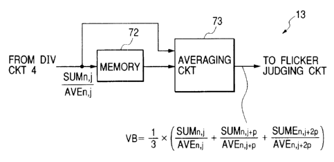
Fig. 13 is a block diagram of the averaging block according to
the eighth embodiment.
The averaging block includes a memory 72 and an averaging
circuit 73. The memory 72 stores the dividing result from the
dividing circuit 4 and when the inputted dividing result is jth line,
the memory 72 outputs the delayed dividing results at the (j + p)ch
and (j + 2p)th horizontal lines on the same field. The averaging
circuit 73 averages the dividing results of jth, (j + p)th~ and (j + 2p)th
horizontal lines. Thus, the output signal of the averaging block is
given by:
VB = {(SUMn,j/AVEn,j) + (SUMn,j + p/AVEn,j + p) + (SUMn,j
zp/AVEn,j + 2p)} x 1/3
The averaging circuit 73 may be replaced with a median filter
to filter the dividing results on the different horizontal lines at the
same frame showing the same phase in the beat frequency of the
flicker component. The averaged signal is supplied to the flicker
judging circuit 5.
As mentioned above, the dividing results at the horizontal
line showing the same phase of the flicker component at the same
frame are averaged, so that affection in luminance variation level
due to the shot image of the object in the video signal is removed.
<NINTH EMBODIMENT>
An illumination flicker detection apparatus according to a
ninth embodiment has substantially the same structure as that of the
first embodiment. The difference is that a threshold value
CA 02322593 2000-10-06
- 33 -
processing circuit 82 is further provided to the flicker judging circuit
5b: The threshold value processing circuit 82 changes threshold
values in accordance with a shutter speed signal which is also used
for controlling the shutter speed of the imager generating the video
signal supplied to the integration circuit 1.
Fig. 14 is a block diagram of the flicker judging circuit 5b
according to the ninth embodiment.
The threshold value processing circuit 82 changes threshold
values THso-orr, TH6o-oN, THso-OFF, and THso-oFF in accordance with
the shutter speed signal to supply the changed values to the
comparing circuit 22.
Figs. 15A and 15C are graphical drawings showing the
outputs of the dividing circuit 4 when the shutter speed is high and
low, respectively. Figs. 15B and 15D are graphical drawings
showing flicker components detected by the DFT circuit 81 when the
shutter speed is high and low, respectively.
As clearly understood by comparing Fig. 15B with Fig. 15D,
the flicker components are relatively high when the shutter speed is
high but the flicker components are relatively low when the shutter
speed is low. Then, in this embodiment, the threshold values are
set to be high when the shutter speed is high. On the other hand,
when the shutter speed is low, the threshold values are set to be low
in accordance with the shutter speed signal.
Accordingly, the flicker components are judged more
accurately by controlling the threshold values which are compared
with the outputs of the DFT circuit 81. Thus, though the shutter
CA 02322593 2000-10-06
-34-
speed is changed, accurate illumination flicker judgment is provided.
<TENTH EMBODIMENT>
An illumination flicker compensation signal generation
apparatus according to a tenth embodiment has substantially the
same structure as that of the first to ninth embodiments. The
difference is that a flicker compensation signal generation circuit 92
is further provided in addition to the illumination flicker detection
apparatus according to the first to ninth embodiments.
Fig. 16 is a block diagram of an imaging apparatus according
to the tenth embodiment. In Fig. 16, the flicker compensation signal
generation apparatus 90 is structured as a portion of the imaging
apparatus.
The imaging apparatus includes an imaging device 93 such as
MOS type imaging element, an AGC (automatic gain control)
amplifier 94, an a/d converter 95, the flicker compensation signal
generation apparatus 90, and a driving circuit 96. The flicker
compensation signal generation apparatus 90 includes the flicker
detection circuit 91 and the flicker compensation signal generation
circuit 92.
The imaging device 93 takes an image and generates the video
signal. Particularly, the imaging device 93 takes an image of an
object under illumination of which luminance varies with the
periodical voltage variation of the ac line. The imaging device is
driven by the driving circuit 96. The AGC amplifier 94 amplifies
the video signal from the imaging device 93 with its gain controlled
in accordance with an AGC gain control signal. The a/ d converter
CA 02322593 2000-10-06
-35-
95 converts the video signal from the AGC amplifier 94 into a digital
video signal. A flicker detection circuit 91 detects illumination
flicker from the digital video signal as mentioned in the first to ninth
embodiments. The flicker compensation signal generation circuit 92
performs illumination flicker compensation with the digital video
signal from the a/d converter 95 and the detection result of the
flicker detection circuit 91 by generating a shutter speed control
signal supplied to the driving circuit 96 and the AGC gain control
signal supplied to the AGC amplifier 94.
Fig. 17 depicts a flow chart showing the operation of the
flicker compensation signal generation circuit 92.
In step s1, when the flicker compensation signal generation
circuit 92 detects power-on, the flicker compensation signal
generation circuit 92 sets the mode of illumination flicker
compensation to 50 Hz in step s2. Next, the flicker compensation
signal generation circuit 92 repeatedly executes the operation in the
loops including the steps s3 to s10.
In step s3, the flicker compensation signal generation circuit
92 obtains the video level of the digital video signal. In the
following step s4, the flicker compensation signal generation circuit
92 determines the AGC gain and the shutter speed and generates the
AGC gain control signal and the shutter speed control signal. In
step s5, the flicker compensation signal generation circuit 92 obtains
the illumination flicker detection result. In the following step s6,
the flicker compensation signal generation circuit 92 judges whether
the illumination flicker frequency is 50 Hz. If the illumination
CA 02322593 2000-10-06
-36-
flicker frequency is 50 Hz, the flicker compensation signal generation
circuit 92 sets the mode of illumination flicker compensation to 50
Hz in step s8.
If the illumination flicker frequency is not 50 Hz in step s6,
the flicker compensation signal generation circuit 92 judges whether
the illumination flicker frequency is 60 Hz in step s7. If the
illumination flicker frequency is 60 Hz in step s7, the flicker
compensation signal generation circuit 92 sets the mode of the
illumination flicker to 60 Hz in step s9. If the illumination flicker
frequency is not 60 Hz in step s7, the flicker compensation signal
generation circuit 92 holds the mode as it is. After steps s8, s9, and
s10, processing returns to step s3.
Figs. 18A and 18B are graphical drawings showing the gain
controlling and the shutter controlling referred in tenth and fifteenth
embodiments.
The flicker compensation signal generation circuit 92 controls
the shutter speed and the AGC gain as shown in Figs. 18A and 18B in
the 50 Hz mode.
The flicker compensation signal generation circuit 92 obtains
brightness in the video image of the digital video signal and
determines the AGC gain and the shutter speed in accordance with
the detected brightness and the flicker judgment result. In Fig. 18A,
"MIN" indicates the minimum value of the AGC gain and the "MAX"
indicates the maximum value of the AGC gain.
When brightness is low, the shutter speed is determined in
accordance with the frame frequency (e.g., 30 Hz) and the frequency
CA 02322593 2000-10-06
-37-
of the ac line voltage (e.g., 50 Hz). Thus, in the low brightness
condition, the shutter speed (interval) is 3/ 100 sec which is the
lowest one of values which are integer times a half cycle of the ac
line voltage.
With increase in the brightness, the AGC gain is gradually
reduced. When the AGC gain reaches the minimum of the AGC
gain as shown in Fig. 18A, the flicker compensation signal generation
circuit 92 instantaneously changes the shutter speed (interval) to
2/100 sec as shown in Fig. 18B. At the same time, the flicker
compensation signal generation circuit 92 changes the shutter speed
to 3/2 times the minimum value, wherein "3/2" is an inverse number
of the changing rate of the shutter speed. This prevents the rapidly
changing in the brightness in the reproduced video image around
shutter speed changing instance.
With further increase in the brightness, the AGC gain is
gradually reduced again. When the AGC gain reaches the minimum
of the AGC gain again, the flicker compensation signal generation
circuit 92 instantaneously changes the shutter speed (interval) to
1/100 sec. At the same time, the flicker compensation signal
generation circuit 92 changes the shutter speed to twice the
minimum value which is an inverse number of the changing rate of
the shutter speed.
When the shutter speed reaches the maximum shutter speed
without flicker, that is, 1/100 sec in 50 Hz, and the AGC gain is
minimum, the shutter speed is increased (shutter interval is reduced)
from 1/100 sec. On the other hand, the AGC gain is held. Thus,
CA 02322593 2000-10-06
-38-
the brightness in the video signal is not saturated, so that the
dynamic range can be increased.
Moreover, favorably, hysteresis is provided between the
shutter speed of 1/100 sec and higher shutter speeds (e.g., 1/250 sec).
The operation mentioned above is for the 50 Hz of the ac line.
In the case of 60 Hz, the shutter speed is set to values which are
integer times the half cycle of the ac line voltage, that is, 1/120 sec,
2/ 120 sec, 3/ 120 sec
In the circuit example shown in Fig. 16, the AGC amplifier 94
is provided and the gain controlling is effected in the analog manner.
However, it is also possible that a digital AGC control circuit is
provided after the a/d converter 95 instead the AGC amplifier 94
and the digital AGC control circuit is controlled in accordance with
the AGC gain control signal (data).
In the above-mentioned embodiments, the averaging unit 6
effects averaging with the integrated values of the present frame and
the previous frames. However, it is also possible to average only
integrated values of previous frames.
Moreover, in the above-mentioned embodiments, illumination flicker
is detected with MOS type of imager. However, this invention is
applicable to the video signal generated from CCD imaging devices.
As mentioned above, according to the illumination flicker
detection apparatus and the method of detecting flicker, it is possible
to detect illumination flicker developed during shooting images
under illumination by ac line voltage without affection due to
luminance level change of an object in the images because the video
CA 02322593 2000-10-06
-39-
signal levels in a plurality of frames are averaged and the flicker
existent judgment is effected in accordance with the averaged value.
Moreover, the illumination flicker detection in the case of 60 Hz of ac
lines at the frame frequency of 30 Hz can be provided.
Moreover, the shutter speed and the AGC gain are controlled
in accordance with the video signal level of the inputted video signal
and the detected flicker frequency to compensate brightness change
due to illumination flicker. Moreover, only the shutter speed is
further controlled when the brightness is sufficiently high. This
prevents a trouble in the reproduced image when the brightness is
high.
<ELEVENTH EMBODIMENT>
Fig. 21 is a block diagram of an illumination flicker detection
apparatus according to the eleventh embodiment.
The illumination flicker detection apparatus includes the
integrating circuit 1, the averaging unit 6 including the memory 2b
and the averaging circuit 3, the dividing circuit 11, the flicker
judging circuit 5, and a still portion judging unit 15.
A video signal is inputted to the integrating circuit 1. The
integrating circuit 1 integrates pixel levels in every horizontal line
(unit area) in a frame from the video signal. The memory 2b stores
the integration result over a plurality of frames (fields). The
averaging circuit 3 averages the integration results of horizontal
lines at a plurality of frames (fields) from the integration result from
the integrating circuit 1 and the memory 2b. The dividing circuit 11
divides the integration results of horizontal lines by the averaged
CA 02322593 2000-10-06
-40-
result of horizontal lines, respectively, when the still portion judging
unit 15 detects a still portion. The flicker judging circuit 5 judges
whether flicker exists in the video signal by frequency-analyzing the
dividing results of horizontal lines.
This illumination flicker detection apparatus is provided with
a discrete circuit in this embodiment. However, the illumination
flicker detection apparatus is also provided with a Digital Signal
Processor (DSP), or a computer with a program.
The video signal is generated by a video camera (not shown in
Fig. 21) under illumination of which luminance varies in accordance
with the voltage change of the ac line. That is, an image of an object
illuminated by fluorescent lamps is shot by the video camera.
The integration circuit 1 integrates, accumulates, or averages
the pixel levels (luminance level) at every horizontal line. The
integrating result of ith line of nth frame is represented by SUMn, i as
shown in Fig. 2A. If one frame of the video signal includes 480 lines,
the integration circuit 1 calculates the integration result SUMn,i to
SUMn,4so for i = 1 to 480.
The memory 2b successively stores a predetermined number
of frames (fields) of the integration result. The averaging circuit 3
effects addition or averaging among SUM"-l,i, SUMn-z,~, and SUMn-3,;
from the memory 2b. Fig. 22 shows the summing or averaging
operation from the integration results of the previous frames. The
memory 2b stores the integration result SUM",; and outputs the
integration results SUMn-1, ;, SUMn-2,i, SUMn-3,i at the ith line at frames
n-1 to n-3. The averaging circuit 3d averages (sums) SUMn-i,t,
CA 02322593 2000-10-06
-41 -
SUM"-2,t, and SUMn-3,;. The averaging result is represented as AVn,i.
In this embodiment, the number of the previous frames per one unit
averaging operation is three. However, it is also possible that, at
least, the integration results of more than one previous frames are
added to the integration result of the present frame.
The dividing circuit 11 obtains SUMn,;/AVn,i through
calculation from the output SUMn,, of the integration circuit 1 and
the output AVn,i of the averaging circuit 3d when the still portion
judging unit judges that the block is still. The flicker judging circuit
5 judges whether there is flickering with the dividing result of the
dividing circuit 11. Fig. 23 is a block diagram of the flicker judging
circuit 5 according to the eleventh embodiment. The flicker judging
circuit 5 includes the DFT (Discrete Fourier Transform) circuit 21,
supplied with the integration result SUMn,i and the averaging result
AVn,i, for detecting frequency Component levels and the comparing circuit
22 for comparing the output of the DFT circuit 21 with threshold
values.
The still portion judging unit 15 includes a summing circuit 7,
a memory 8, and a still portion judging circuit 9. The still portions
judging unit 15 detects a still portion at the image on the screen
using the output of the integrations circuit 1.
The summing circuit 7 sums the integration results of lines
included in N cycles of the flicker component at a frame. A portion
of a frame including N cycles of flicker component is referred to as a
still portion judging block. It is assumed that the top line number
at Jth still portion judging block at nth frame is k and the number of
CA 02322593 2000-10-06
-42-
lines in N (natural number) cycles of the flicker component at the
frame is p (natural number). Then, the output B-SUMn~ of the
summing circuit 7 is given by:
B-SUMnj = SUM"k + SUMnk+i + . . . -~-SUMnk+P - i
Fig. 24 is an illustration showing the summing operation
according to the eleventh embodiment, wherein N = 1 and j = 1. As
shown in Fig. 19A to 19D, if the cycle of the ac line used for
illumination is 50 Hz and the frame cycle is 30 Hz, N lies from one to
three.
The summing results of the summing circuit 7 obtained as
mentioned above are the same with respect to periodical variation in
the luminance of the light source.
Fig. 25 is an illustration showing the operation of the still
portion judging circuit 9. The memory 8 temporally stores the
summing results of several frames. The still portion judging circuit
9 calculates difference between the summing result B-SUMn~ of the
present frame from the summing circuit 7 and the one-frame-prior
summing result B-SUMn-1,~ from the memory 8 and compares the
difference with a threshold value TH1. When the difference is lower
than the threshold value THi, the still portion judging circuit 9
judges the block is still portion.
As mentioned above, because the flickers component levels at
the summing results B-SUMn,~ and B-SUMn-1,~ are the same, the
difference represents variation or movement of the image of an
object at the still portion judging block. Therefore, the still portion
judging block is judged to be still when the difference is lower than
CA 02322593 2000-10-06
- 43 -
the threshold value THi.
The dividing circuit 11 calculates division SUMni~AVnl from
the output SUMn; of the integration circuit 1 and the output AVni of
the averaging circuit 3d when the difference is lower than the
threshold value TH1. When the difference is equal to or higher than
the threshold value THi, the dividing circuit 11 does not output the
dividing result.
Fig. 4A shows the output of the dividing circuit 11 according
to the eleventh embodiment, wherein the axis of abscissas represents
line number at a frame and the axis of ordinates represents levels of
dividing results, that is, SUMn,i/AVn,i. The dividing results shows
flickering.
Fig. 4B shows the output of the DFT circuit 21 according to
the first embodiment, wherein the axis of abscissas represents
frequency and axis of ordinates represents levels of frequency
components.
The line Fso represents the level of the DFT circuit 21 at 50 Hz,
i.e., component of 50 Hz and the line F6o represents the level of the
DFT circuit 21 at 60 Hz, i.e., component of 60 Hz.
The comparing circuit 22 compares the results Fso and F6o of
the DFT circuit 21 with threshold levels THso-orr, TH6o-oN, THSO-OFF,
and TH6o-oFF. There are relations, THso-off > THSO-OFF and THso-oN >
TH60-OFF.
Basically, the comparing circuit 22 compares the component
F5o with the threshold levels THSO-oN and THSO-OFF and the component
F6o with the threshold levels THbo-oN and TH6o-oFF to detect flicker in
CA 02322593 2000-10-06
-44-
the video signal.
More specifically, the comparing circuit 22 judges the flicker
as follows:
When (the value of) F5o < THso-oFF and (the value of) F6o <
TH60-OFF, the comparing circuit 22 judges that there is no flicker.
When a X F6o < F5o and F5o > THSO-orr, the comparing circuit
22 judges there is flicker of 50 Hz.
When ~i x Fso < F6o and F6o > TH6o-oN,
the comparing circuit 22 judges there is flicker of 60 Hz.
In other cases, the comparing circuit 22 judges that it is
unknown that there is flicker.
In the above equations, a is a weighting coefficient for
flicker detection of 50 Hz and /3 is a weighting coefficient for
flicker detection of 60 Hz. These coefficients are sufficiently greater
than one, so that if the frequency component Fso (Fso) is greater than
the value of the weighting-coefficient-times the frequency
component F6o (F5o), the comparing circuit 22 judges there is flicker
of 50 Hz (60 Hz). This reduces probability of erroneous judgment of
existence of flicker due to luminance level change within a frame
representing an image.
As mentioned above, according to this embodiment, the
existence of flicker is judged from the average of integration values
over a plurality of frames (fields) including the present frame at the
corresponding lines. Thus, the flicker detection can be provided
without affection of luminance level variation due to motion of the
image. Moreover, this structure (this method) provides
CA 02322593 2000-10-06
-45-
illumination flicker detection of 60 Hz wherein luminance level
variation.
In the eleventh embodiment, the integration circuit 1
integrates the pixel values every horizontal line. However, it is also
possible that the integration circuit 1 integrates the pixel value on
thinned horizontal lines, wherein thinning period is sufficiently
shorter than the period of flicker (beat) component. In this case, the
circuit stage after the integration circuit 1 effects the above-
mentioned operation for the thinned horizontal lines. Thus, the
capacity of the memory 2b can be reduced.
In this embodiment, the still portion judging unit 15 supplies
the result of still portions to the dividing circuit 11. However, it is
also possible to use the result in the flicker judging circuit 5.
<TWELFTH EMBODIMENT>
An illumination flicker detection apparatus according to a
twelfth embodiment has substantially the same structure as that of
the eleventh embodiment. The difference is that the integrating
circuit 1d effects integration every a plurality of horizontal lines in
which the flicker component level is considered to be substantially
the same. That is, the video (luminance) levels of pixels are
integrated every adjacent or consecutive lines.
Fig. 26 is an illustration showing the operation of the
integration circuit 1d according to the twelfth embodiment.
As shown in Fig. 26, the integration circuit 1d integrates or
averages the video (luminance) level of pixels every block (in the
drawing, left portions of the two consecutive horizontal lines) in
. CA 02322593 2000-10-06
-46-
which the flicker component level is considered to be substantially
the same. Here, the area at which the flicker component level is
considered to be substantially the same is referred to as a block.
The integrated or averaged value of the video level of all effective
pixels at the ith block at nth frame is represented by SUMn,b;.
Fig. 27 is an illustration showing the summing or averaging
operation from the integration results of the present frame and the
previous frames. The memory 2b stores the integration result
SUM",tt and outputs the integration results SUMn-i, bc, SUMn-z,bi,
SUMn-3,bi at the ith block at frames n-1 to n-3. The averaging circuit
3d, shown in Fig. 21, averages (sums) SUMn_l,i, SUM"-Z,;, and SUM"_3,;.
The averaging result is represented as AVn,;. In this embodiment,
the number of the previous frames per one unit averaging operation
is three. However, it is also possible that, at least, the integration
results of more than one previous frames are summed.
Fig. 28 is an illustration showing the summing operation
according to the twelfth embodiment. The summing circuit 7
sums the integration results of horizontal lines at the still portion
judging block corresponding to N cycles of the flicker component at
a frame. The summing circuit 7 sums the integration results of q
blocks at jth still portion judging block. It is assumed that the
number of the top block is m. The output B-SUMnbj is given by:
B-SUMnbj =SUMnm + SUMnn,+~ + ' ' ' +SUMnn,+q_i
As described in the eleventh embodiment, N is a natural
number from 1 to 3 when the ac line frequency is 50 Hz and the
frame frequency is 30 Hz. Fig. 28 shows the condition that N = 1
CA 02322593 2000-10-06
-47-
and j = 1. The summing result of the blocks (horizontal lines)
corresponding to N cycle of the flicker component shows the same
luminance level with respect to the flickering.
Fig. 29 is an illustration showing the still portion judging
operations according to the twelfth embodiment. The still portion
judging circuit 9 calculates difference between the summing result B-
SUMnb~ and the one-frame-prior summing result B-SUMn-i read from
the memory 8 and compares the difference with the threshold value
THi. When the difference is lower than the threshold value THi the
still portion judging circuit 9 judges the still portion judging block is
in the still condition.
The still portion judging circuit 9 supplies the judging result
to the dividing circuit 11. The dividing circuit 11 calculates
SUMnbi/AVnbi only when the still portion judging block is judged to
be still. The flicker judging circuit 5 judges the existence of flicker
in accordance with the result SUMnbi/ AVnbi of the dividing circuit 11
as mentioned above.
This embodiment is effective for video signals obtained from
imagers using color filters. Figs. 6A and 6B show arrangements of
color filters for single plate imagers and processing in this
embodiment. The arrangement shown in Fig. 6A is for the
complementary filter structure and the arrangement shown in Fig. 6B
is a portion of Bayer arrangement for primary color filter structure.
As shown in Figs. 6A and 6B, different color filters are arranged and
adhered on imagers.
In the complementary color filter type of imager, a first line
CA 02322593 2000-10-06
- 48 -
and a second line are alternately arranged, wherein a cyan filter Cy
and a yellow filter Ye are alternately arranged every pixel on the
first line and a magenta filter Mg and a green filter are alternately
arranged every pixel on the second line. In the integrating the
video levels of pixels in two consecutive lines, four pixels
surrounded with a chain line are dealt as one block. The video
signal level in one block is represented as
Cy+Mg+Ye+G=2R+3G+2B . Y
Then, the video signal level in one block provides
substantially the same level as the luminance signal. This signal
similar to the luminance signal is integrated and the integrated result
is used for detecting flicker, so that accurate flicker detection is
provided.
In the arrangement shown in Fig. 6B, one line where R and G
filters are alternately arranged and another line where G and B filters
are alternately arranged. In integration on these two lines, four
pixels surrounded by a chain line are dealt as one block and values
in a plurality of blocks are integrated. The video signal level in one
block is represented as
R+G+G+B=R+2G+B - Y
Thus, the video signal level in one block is substantially the
same as the luminance signal Y. This video signal similar to the
luminance signal is integrated every a plurality of horizontal lines
(two lines), so that accurate flicker detection is provided.
As mentioned above, according to the twelfth embodiment,
the integration of video signal levels is effected every area in which
CA 02322593 2000-10-06
-49-
flicker components can be considered as substantially the same.
Further, the integration results are summed every still portion
judging block and the difference between the summing results of the
present frame and the previous frame is calculated. Only when the
difference is lower than the threshold THi, the dividing circuit effect
dividing. The flicker judging circuit 5 judges the existence of flier
in accordance with the dividing result.
In this embodiment, the still portion judging circuit 9 controls
the dividing circuit 11. However, the still portion judging circuit 9
may control the flicker judging circuit 5. That is, division is
effected irrespective of the still portion judging result. The flicker
judging circuit 5 judges (outputs) the existence of flier only when the
still portion judging block is judged to be still. Moreover, the
outputting result of the flicker judging circuit 5 may be controlled in
accordance with the output of the still portion judging circuit 9.
<THIRTEENTH EMBODIMENT>
An illumination flicker detection apparatus according to a
thirteenth embodiment has substantially the same structure as that of
the eleventh embodiment. The difference is that a dividing circuit
32 is further provided in the still portion judging unit 15.
Fig. 30 is a block diagram of the still portion judging circuit
9b. The still portion judging circuit 9b includes a difference
calculating circuit 31, a dividing circuit 32, and a comparing circuit
32.
The difference calculating circuit 31 calculates a difference
between the summing result B-SUM" of the present frame and the
CA 02322593 2000-10-06
-50-
summing result of the one-frame-previous frame B-SUMn-ij. The
dividing circuit 32 divides the difference from the difference
calculation circuit 31 by the summing result from the summing
circuit 7. The dividing result is supplied to the comparing circuit 33.
The dividing result is given by:
~ B-SUMnj-B-SUMn-lj ~ ~ B-SUMnj
The comparing circuit 33 compares the dividing result with a
threshold value THz. When the dividing result is lower than the
threshold value THz, the Jth still portion judging block is judged to be
l0 still by the comparing circuit 33. The judging result of the still
portion judging unit 15, i.e., the output of the comparing circuit 33 is
supplied to the dividing circuit 11. The dividing circuit 11 and the
flicker judging circuit 5 judges flicker as similarly as the eleventh
embodiment.
In the thirteenth embodiment, the ratio between the summing
result of the present frame and the one-frame-previous summing
result and the ration, that is, the dividing result is compared with the
threshold THz. Thus, though the video signal level varies, accurate
still portion judgment is provided, so that the flicker detection can
be more accurately provided.
<FOURTEENTH EMBODIMENT>
An illumination flicker detection apparatus according to a
fourteenth embodiment has substantially the same structure as that
of the thirteenth embodiment. The difference is that an averaging
circuit 41 and a difference calculation circuit 42 are further provided
in the still portion judging circuit 9c.
CA 02322593 2000-10-06
-Sl-
Fig. 31 is a block diagram of the still portion judging unit 15
according to the fourteenth embodiment. The still portion judging
unit 15 includes the averaging circuit 41 for averaging the summing
result of the summing circuit 7 and the one-frame-previous summing
result and two-frame-previous summing result from the memory 8,
the difference calculating circuit 42 for calculating a difference
between the summing result of the present frame and the averaging
result B-AVEnj of the averaging circuit 41, a dividing circuit 43 for
dividing the difference by the summing result of the present frame,
and a comparing circuit 44 compares the dividing result from the
dividing circuit 43 with a. threshold TH3.
The averaging circuit 41 averages the summing result B-SUM"j
of the present frame and the one-frame-previous summing result B-
SUMn-ij and two-frame-previous summing result B-SUMn-2j from the
memory 8 to output an averaging result B-AVE"j which is given by:
B-AVEnj = (B-SUMnj + B-SUMn-lj + B-SUMn-2I) x 1/3
The difference calculating circuit 42 calculates a difference
between the summing result B-SUM"j of the present frame and the
averaging result AVEnj of the averaging circuit 41. The dividing
2o circuit 43 divides the difference by the summing result B-SUMnj of
the present frame. The dividing result is given by:
~ B-SUMnj - B-AVEnj ~ / B-SUMnj
The comparing circuit 44 compares the dividing result from
the dividing circuit 43 with a threshold TH3. When the dividing
result is lower than the threshold TH3, the still portion judging unit
15 judges the still portion judging block is still. The judging
CA 02322593 2000-10-06
-52-
result of the still portion judging unit 15, i.e., the output of the
comparing circuit 44 is supplied to the dividing circuit 11. The
dividing circuit 11 and the flicker judging circuit 5 judges flicker as
similarly as the eleventh embodiment.
In the thirteenth embodiment, a ratio between the summing
result B-SUMn~ of the present frame and the averaging result B-AVEn~
derived by averaging the previous frames of summing results and
the ratio is compared with the threshold TH3, so that video level of
the previous frames to be compared with that of the present frame
becomes stable. Thus, the still portion can be more accurately
judged. As the result, accuracy of flicker detection at 50 Hz and 60
Hz is improved.
Moreover, in the dividing circuit 43, the difference is divided
by the summing result B-SUMn~ of the present frame. However,
dividing the averaging result B-AVEnj instead the summing result B-
SUMnj of the present frame provides the similar effect. Moreover,
the averaging circuit 41 may be provided with the circulation type of
filter or the FIR filter.
<FIFTEENTH EMBODIMENT>
An illumination flicker compensation signal generation
apparatus according to a fifteenth embodiment has substantially the
same structure as that of the eleventh to fourteenth embodiments.
The difference is that a flicker compensation signal generation circuit
192 is provided in addition to the illumination flicker detection
apparatus 190 according to the eleventh to fourteenth embodiments.
Fig. 32 is a block diagram of an imaging apparatus according
CA 02322593 2000-10-06
- 53 -
to the fifteenth embodiment. In Fig. 32, the flicker compensation
signal generation apparatus 190 is structured as a portion of the
imaging apparatus.
The imaging apparatus includes an imaging device 193 such
as MOS type imaging element, an AGC (automatic gain control)
amplifier 194, an a/d converter 195, the flicker compensation signal
generation apparatus 190, and a driving circuit 196. The flicker
compensation signal generation apparatus 190 includes the flicker
detection circuit 191 and the flicker compensation signal generation
circuit 192.
The imaging device 193 takes an image and generates the
video signal. Occasionally, the imaging device 193 takes an image
of an object under illumination of which luminance varies with the
periodical voltage variation of the ac line. The imaging device 193
is driven by the driving circuit 196. The AGC amplifier 194
amplifies the video signal from the imaging device 193 with its gain
controlled in accordance with an AGC gain control signal. The a/d
converter 195 converts the video signal from the AGC amplifier 194
into a digital video signal. A flicker detection circuit 191 detects
illumination flicker from the digital video signal as mentioned in the
eleventh to fourteenth embodiments. The flicker compensation
signal generation circuit 192 performs illumination flicker
compensation with the digital video signal from the a/d converter
195 and the detection result of the flicker detection circuit 191 by
generating a shutter speed control signal supplied to the driving
circuit 196 and the AGC gain control signal supplied to the AGC
CA 02322593 2000-10-06
-54-
amplifier 194.
Fig. 33 depicts a flow chart showing the operation of the
flicker compensation signal generation circuit 192 according to the
fifteenth embodiment.
In step s11, when the flicker compensation signal generation
circuit 192 detects power-on, the flicker compensation signal
generation circuit 192 sets the mode of illumination flicker
compensation to 50 Hz in step s12. Next, the flicker compensation
signal generation circuit 192 repeatedly executes the operation in the
loops including the steps s13 to s20.
In step s13, the flicker compensation signal generation circuit
192 obtains the video level of the digital video signal. In the
following step s14, the flicker compensation signal generation circuit
192 determines the AGC gain and the shutter speed and generates
the AGC gain control signal and the shutter speed control signal. In
step s15, the flicker compensation signal generation circuit 192
obtains the illumination flicker detection result. In the following
step s16, the flicker compensation signal generation circuit 192
judges whether the illumination flicker frequency is 50 Hz. If the
illumination flicker frequency is 50 Hz, the flicker compensation
signal generation circuit 192 sets the mode of illumination flicker
compensation to 50 Hz in step s18.
If the illumination flicker frequency is not 50 Hz in step s16,
the flicker compensation signal generation circuit 192 judges whether
the illumination flicker frequency is 60 Hz in step s17. If the
illumination flicker frequency is 60 Hz in step s17, the flicker
CA 02322593 2000-10-06
-55-
compensation signal generation circuit 192 sets the mode of the
illumination flicker to 60 Hz in step s19. If the illumination flicker
frequency is not 60 Hz in step s17, the flicker compensation signal
generation circuit 192 holds the mode as it is. After steps s18, s19,
and s20, processing returns to step s13.
Figs. 18A and 18B show the gain controlling and the shutter
controlling operation which was also referred in tenth embodiment.
The flicker compensation signal generation circuit 192
controls the shutter speed and the AGC gain as shown in Figs. 18A
and 18B in the 50 Hz mode.
The flicker compensation signal generation circuit 192 obtains
brightness in the video image of the digital video signal and
determines the AGC gain and the shutter speed in accordance with
the detected brightness and the flicker judgment result. In Fig. 18A,
"MIN" indicates the minimum value of the AGC gain and the "MAX"
indicates the maximum value of the AGC gain.
When brightness is low, the shutter speed is determined in
accordance with the frame frequency (e.g., 30 Hz) and the frequency
of the ac line voltage (e.g., 50 Hz). Thus, in the low brightness
condition, the shutter speed (interval) is 3/100 sec which is the
lowest one of values which are integer times a half cycle of the ac
line voltage.
With increase in the brightness, the AGC gain is gradually
reduced. When the AGC gain reaches the minimum of the AGC
gain as shown in Fig. 18A, the flicker compensation signal generation
circuit 192 instantaneously changes the shutter speed (interval) to
CA 02322593 2000-10-06
-56-
2/100 sec as shown in Fig. 18B. At the same time, the flicker
compensation signal generation circuit 192 changes the shutter speed
to 3/2 times the minimum value, wherein "3/2" is an inverse number
of the changing rate of the shutter speed. This prevents the rapidly
changing in the brightness in the reproduced video image around
shutter speed changing instance.
With further increase in the brightness, the AGC gain is
gradually reduced again. When the AGC gain reaches the minimum
MIN of the AGC gain again, the flicker compensation signal
generation circuit 192 instantaneously changes the shutter speed
(interval) to 1/100 sec. At the same time, the flicker compensation
signal generation circuit 192 changes the shutter speed to twice the
minimum value which is an inverse number of the changing rate of
the shutter speed.
When the shutter speed reaches the maximum shutter speed
without flickering, that is, 1/100 sec in 50 Hz, and the AGC gain is
minimum, the shutter speed is increased (shutter interval is reduced)
from 1/100 sec. On the other hand, the AGC gain is held. That is,
only the shutter speed is controlled for brightness control. Thus,
the brightness in the video signal is not saturated, so that the
dynamic range can be expanded.
Moreover, favorably, hysteresis is provided between the
shutter speed of 1/100 sec and higher shutter speeds (e.g., 1/250 sec).
The operation mentioned above is for the 50 Hz of the ac line.
In the case of 60 Hz, the shutter speed is set to values which are
integer times the half cycle of the ac line voltage, that is, 1/120 sec,
CA 02322593 2000-10-06
-57-
2/120 sec, 3/120 sec
In the circuit example shown in Fig. 32, the AGC amplifier 194
is provided and the gain controlling is effected in the analog manner.
However, it is also possible that a digital AGC control circuit is
provided after the a/ d converter 195 instead the AGC amplifier 194
and the digital AGC control circuit is controlled in accordance with
the AGC gain control signal (data).
In the above-mentioned embodiments, the averaging unit 3d
effects averaging with the integrated values of the previous frames.
However, it is also possible to average integrated values of previous
frames and the present frame.
Moreover, in the above-mentioned embodiments, illumination
flicker is detected with MOS type of imager. However, this
invention is applicable to the video signal generated from CCD
imaging devices.
As mentioned above, according to the illumination flicker
detection apparatus and the method of detecting flicker according to
eleventh to fifteenth embodiments, it is possible to detect
illumination flicker developed during shooting images under
illumination by ac line voltage without affection due to luminance
level change of an object in the images because the flicker is detected
at the portion where the image is judged to be still. Thus, flickers
due to 50 Hz ac line voltage and
60 Hz line voltage are automatically detected, respectively. Thus,
the flicker compensation is provided.
Moreover, the shutter speed and the AGC gain are controlled
CA 02322593 2000-10-06
-58-
in accordance with the video signal level of the inputted video signal
and the detected flicker frequency to compensate brightness change
due to illumination flicker. Moreover, only the shutter speed is
further controlled when the brightness is sufficiently high. This
prevents a trouble in the reproduced image when the brightness is
high. That is, when an incident light amount increases, shooting the
object image at a higher shutter speed prevents saturation in the
video level.
<SIXTEENTH EMBODIMENT>
Fig. 34 is a block diagram of an ac line frequency detection
apparatus according to a sixteenth embodiment.
The ac line frequency detection circuit has substantially the
same structure as the illumination flicker detection apparatus
according to the first embodiment. The difference is that an ac line
frequency detection circuit 32 replaces the flicker judging circuit 5.
The ac line frequency detection apparatus includes the
integrating circuit 1, the averaging unit 6 including the memory 2
and the averaging circuit 3, the dividing circuit 4, and an ac line
frequency detection circuit 32.
A video signal is inputted to the integrating circuit 1. The
integrating circuit 1 integrates pixel levels in every horizontal line
(nit area) in a frame from the video signal. The memory 2 stores the
integration result over a plurality of frames (fields). The averaging
circuit 3 averages the integration results of horizontal lines at a
plurality of frames (fields) from the integration result from the
integrating circuit 1 and the memory 2. The dividing circuit 4
CA 02322593 2000-10-06
-59-
divides the integration results of horizontal lines by the averaged
result of horizontal lines, respectively. The ac line frequency
detection circuit 32 detects the frequency of an ac line voltage in
accordance with the dividing results of horizontal lines.
This ac line frequency detection apparatus is provided with a
discrete circuit in this embodiment. However, the ac line frequency
detection apparatus is also provided with a Digital Signal Processor
(DSP), or a computer with a program.
The video signal is generated by a video camera (not shown in
Fig. 1) under illumination of which luminance varies in accordance
with the voltage change of the ac line. That is, an image of an object,
illuminated by fluorescent lamps, is shot by a video camera.
The integration circuit 1 integrates, accumulates, or averages
the pixel levels (luminance level) at every horizontal line. The
integrating result of ith line of nth frame is represented by SUMn; as
shown in Fig. 2A. If one frame of the video signal includes 480
horizontal lines, the integration circuit 1 calculates the integration
results SUMn,i to SUMn,4so for i = 1 to 480.
The memory 2 successively stores a predetermined number of
frames (fields) of the integration results. The averaging circuit 3
effects addition or averaging among SUM",i from the integration
circuit 1, SUMn-1,,, SUMn-2,i~ and SUMn-3,; from the memory 2. Fig.
2B shows the summing or averaging operation from the integration
results of the present frame and the previous frames. The memory 2
stores the integration result SUMn,i and outputs the integration
results SUMn-i, ;, SUM"-2,t, SUMn-3,i at the ith line at frames n-1 to n-3.
CA 02322593 2000-10-06
-60-
The averaging circuit 3 averages (sums) SUM";, SUMn-i,i~ SUMn-2,i~
and SUM"-3,i. The averaging result is represented as AVEn,i. In
this embodiment, the number of the previous frames per one unit
averaging operation is three. However, it is also possible that, at
least, the integration results of more than one previous frames are
added to the integration result of the present frame.
The dividing circuit 4 obtains SUMn,;/ AVEn,; through
calculation from the output SUMn,i of the integration circuit 1 and
the output AVEn,i of the averaging circuit 3a. The flicker judging
circuit 5 judges whether there is flickering with the dividing result of
the dividing circuit 4.
The ac line frequency detection circuit 32 judges the existence
of illumination flicker in the video signal generated with
illumination using the ac line voltage and detects frequency of the ac
line from the feature of the variation in the result of the dividing
circuit 4. More specifically the ac line frequency detection circuit 32
detects the ac line frequency by analyzing the waveform of the
variation in the result of the dividing circuit 4.
Fig. 35 is a graphical drawing illustrating the ac line
frequency operation according to the sixteenth embodiment. Fig. 36
depicts a flow chart showing the ac line frequency operation
according to the sixteenth embodiment.
The ac line frequency detection circuit 32 obtains the dividing
result from the dividing circuit 4 in step s21. Next, the ac line
frequency detection circuit 32 detects crossing points di (i = 1...) at
which the variation in the division result crosses level 1.0 in step s22.
CA 02322593 2000-10-06
-61 -
The ac line frequency detection circuit 32 calculates intervals (the
number of lines in the interval) between the two consecutive crossing
points (d1 and d2, d2 and d3...) in step s23 as shown in Fig. 35.
In the following step s24, the ac line frequency detection
circuit 32 resets its count CNT to zero. Next, the ac line frequency
detection circuit 32 judges whether each of interval includes a half of
lines corresponding to one cycle of flicker component to judge that
the flicker frequency is developed by the ac line voltage of 50 Hz in
steps 25 and 26.
Here, the theoretical number of the horizontal lines
corresponding to one cycle of the flicker component is calculated
from the frame frequency, the number of horizontal lines per frame,
and the ac line frequency.
In step 26, the ac line frequency detection circuit 32 judges
that the interval includes a half of horizontal lines corresponding to
one cycle of the flicker component of 50 Hz when the number of
horizontal lines lies within an allowable range from FREQ 50 MIN to
FREQ 50 MAX to provide tolerance.
If the interval includes a half of horizontal lines
corresponding to one cycle of the flicker component of 50 Hz, the ac
line frequency detection circuit 32 increments its count CNT in step
s27 and processing returns to step s25 to repeat the operation in
steps s25 to s27 for all lines in one frame.
In step s25, if all intervals of crossing points within one frame
have been judged, processing proceeds to step s28.
In step s28, the ac line frequency detection circuit 32 compares
CA 02322593 2000-10-06
-62-
the counts CNT with a threshold TH4 in step s28. If the count CNT
is higher than the threshold TH4, the ac line frequency detection
circuit 32 judges that there is flicker of 50 Hz in this frame in step s29.
If the count CNT is not higher than the threshold TH4, the ac line
frequency detection circuit 32 judges that there is no flicker of 50 Hz
in this frame in step s30 and detects that there is other flicker (for
example, 60 Hz) as similar to the operation represented by steps s21
to s29.
After processing in steps s29 and s30, the ac line frequency
detection circuit 32 returns to step s21 through the step s31 to repeat
the above-mentioned operation of the next frame.
As mentioned above, the video levels of pixels at a frame of
the video signal generated with illumination varying with the ac line
voltage variation are integrated. The integrated results of frames,
including the present frame, are averaged with respect to
corresponding horizontal lines. The integration result of each line
is divided by the averaging result of each line. The ac line
frequency is judged from the frequency analyzing the variation in
the dividing results. Thus, the ac line frequency measurement is
possible without directly detecting the ac line voltage or ac current
from an ac outlet.
Moreover, because the judgment is effected using the average
between a plurality of frames, the ac line frequency is accurately
measured without affection of luminance level variation due to
movement of an object in the screen of the video signal.
<SEVENTEENTH EMBODIMENT>
CA 02322593 2000-10-06
- 63 -
Fig. 37 is a block diagram of an ac line frequency detection
apparatus according to a seventeenth embodiment.
The ac line frequency detection apparatus has substantially
the same structure as that according to the sixteenth embodiment.
The difference is that an ac line frequency detection circuit 33
replaces the ac line frequency detection circuit 32.
Fig. 38 is a block diagram of the ac line frequency detection
circuit 33.
The ac line frequency detection circuit 33 includes the DFT
(Discrete Fourier Transform) circuit 21, supplied with the division
result STJIVIn,i ~AVn,i, for detecting frequency Component levels and the
comparing circuit 22 for comparing the output of the DFT circuit 21
with threshold values.
The DFT circuit 21 supplied with the division result SUM",,
/ AVn,i and the comparing circuit 22 for comparing the output of the
DFT circuit 21 with threshold values.
Fig. 4A shows the output of the dividing circuit 4, wherein the
axis of abscissas represents line number at a frame and the axis of
ordinates represents levels of dividing results, that is, SUMn,i~ AVn,i.
The dividing results shows flicker.
Fig. 4B shows the output of the DFT circuit 21, wherein the
axis of abscissas represents frequency and axis of ordinates
represents levels of frequency components.
The DFT circuit 21 effects Discrete Fourier Transform
operation to output frequency components as shown in Fig. 4B from
the division result of the division circuit 4.
CA 02322593 2000-10-06
-64-
The line Fso represents the level of the DFT circuit 21 at 50 Hz,
i.e., component of 50 Hz and the line F6o represents the level of the
DFT circuit 21 at 60 Hz, i.e., component of 60 Hz.
The comparing circuit 22 compares the results Fso and Fbo of
the DFT circuit 21 with threshold levels THso-oN, THso-oN, THso-oFF,
and THbo-oFF. There are relations, THso-oN > THso_oFF and TH6o-orr >
TH60-OFF.
Basically, the comparing circuit 22 compares the component
Fso with the threshold levels THso-oN and THso-oFF and the component
F6o with the threshold levels TH6o-oN and TH6o-oFF to detect flicker in
the video signal.
More specifically, the comparing circuit 22 judges the flicker
as follows:
When (the value of) Fso < THso-oFF and (the value of) F6o <
THso-oFF, the comparing circuit 22 judges that there is no flicker.
When a x Fbo < Fso and Fso > THso-oN, the comparing circuit
22 judges there is flicker of 50 Hz.
When /3 x Fso < F6o and F6o > TH6o-orr,
the comparing circuit 22 judges there is flicker of 60 Hz.
In other cases, the comparing circuit 22 judges that it is
unknown that there is flicker.
In the above equations, ce is a weighting coefficient for
flicker detection of 50 Hz and ~i is a weighting coefficient for
flicker detection of 60 Hz. These coefficients are sufficiently greater
than one, so that if the frequency component Fso (F6o) is greater than
the value of the weighting-coefficient-times the frequency
CA 02322593 2000-10-06
-65-
component F6o (Fso), the comparing circuit 22 judges there is flicker
of 50 Hz (60 Hz). This reduces probability of erroneous judgment of
existence of flicker due to luminance level change within a frame
representing an image.
As mentioned above, according to this embodiment, the
existence of flicker is judged from the average of integration values
over a plurality of frames (fields) including the present frame at the
corresponding lines. Thus, the flicker detection can be provided
without affection of luminance level variation due to motion of the
image. Moreover, this structure (this method) provides
illumination flicker detection of 60 Hz wherein luminance level
variation.
In this embodiment, the integration circuit 1 integrates the
pixel values every horizontal line. However, it is also possible that
the integration circuit 1 integrates the pixel value on thinned
horizontal lines, wherein thinning period is sufficiently shorter than
the period of flicker (beat) component. In this case, the circuit stage
after the integration circuit 1 effects the above-mentioned operation
for the thinned horizontal lines. Thus, the capacity of the memory
2b can be reduced.
According to this embodiment, the ac line frequency detection
apparatus includes the DFT circuit 21 and the comparing circuit 22,
so that the presence of illumination flicker at one of various ac line
frequencies can be detected substantially at the same time.
<EIGHTEENTH EMBODIMENT>
Fig. 39 is an ac line frequency detection apparatus according
CA 02322593 2000-10-06
-66-
to an eighteenth embodiment. The ac line frequency detection
apparatus according to the eighteenth embodiment has substantially
the same structure as that according to the sixteenth embodiment or
the seventeenth embodiment. The difference is that an imaging
circuit 200 is further provided. The imaging circuit 200 includes an
imaging element and a driving circuit (not shown). The imaging
circuit 200 generates and supplies the video signal to the integrating
circuit 1. The memory 2, the averaging circuit 3, dividing circuit 4,
and the ac line frequency detection circuit 32 (33) detect ac line
frequency as mentioned above. Thus, the ac line frequency
detection apparatus according to the nineteenth embodiment can
indirectly detect the existence of illumination flicker and the
frequency of the illumination flicker from the image without directly
detecting the ac line voltage or ac line current from the ac outlet.
Moreover, because the ac line frequency detection apparatus
according to the eighteenth embodiment includes the imaging circuit,
so that there is no necessity of a unit generating the video signal and
the cable for supplying the video signal to the integrating circuit 1.