Note: Descriptions are shown in the official language in which they were submitted.
CA 02322735 2002-06-21
PATCH ANTENNA USING NON-CONDUCTIVE FRAME
Background of the Invention
1. Field of the Invention
The present invention relates to antennas; more particularly, patch antennas.
2. Description of the Prior Art
FIG. 1 illustrates an exploded view of a prior art patch antenna assembly.
Non-conductive front housing 10 and conductive rear housing 12 form the outer
surfaces of the antenna assembly. The two sections of the housing enclose
multi-
layered feedboard 14, resonators 16 and 18 and spacers 20. Spacers 20 are
attached
1o to front side 22 of feedboard 14 by screws 24. Screws 24 mate with threads
on the
inside of spacers 20 by passing through holes 26 in feedboard 14. Resonators
16
and 18 are attached to spacers 20 in a similar fashion. Screws 28 mate with
threads
on the inside of spacers 20 by passing through holes 30 in resonators 16 and
18. The
spacers are chosen so that they provide a space of approximately 1/10 of a
wavelength at the frequency of operation between feedboard 14 and resonators
16
and 18. The assembled feedboard, spacers and resonators are mounted inside of
the
enclosure formed by front housing 10 and rear housing 12. A signal to be
transmitted by the antenna assembly is provided to conductor 40 of multi-
layered
feedboard 14. Conductor 40 is typically positioned on one layer of feedboard
14
2o such as on top layer 42. An insulating layer is typically provided between
conductor
40 and a ground plane layer of feedboard 14. The ground plane layer 22
normally
has openings or slots 44 which allow the signal from conductor 40 to couple to
resonators 16 and 18 so that the signal can be transmitted through front
housing 10.
FIG. 2 provides a more detailed illustration of the assembled feedboard 14,
spacers 20 and resonators 16 and 18. Screws 24 pass through holes in feedboard
14
CA 02322735 2002-06-21
to mate with the threaded inside portion of spacer 20. Similarly, screws 28
pass
through holes in resonators 16 and 18 to mate with the threaded inside portion
of
spacers 20.
This prior art patch antenna assembly suffers from several shortcomings.
The assembly is expensive to assemble because of the many individual parts
such as
eight spacers and 16 screws. The spacers are expensive to mass produce because
they include threaded inner portions. Additionally, the holes made through
resonators 16 and 18 to allow screws 28 to mate with spacers 20 create
unwanted
patterns in the radio frequency energy radiated by the antenna assembly. For
to example, if the antenna is being used for a horizontally polarized
transmission, the
holes introduce additional non-horizontal polarizations in the transmitted
signal.
Summary of the Invention
The present invention solves the aforementioned problems by providing a
non-conductive frame that supports the resonators. The frame supports the
resonators without making holes in the resonators and thereby avoids the
problem of
creating unwanted electric field polarizations. Additionally, the frame grasps
the
resonators in areas of low current density and thereby avoids creating
additional
disturbances in the radiation pattern. In another embodiment of the invention,
the
frames include posts that are used to attach the frames to the feedboard
without
2o using additional components such as screws.
In accordance with one aspect of the present invention there is provided an
antenna assembly, comprising: a signal feedboard having a ground plane with an
opening and a signal conductor positioned across the opening; a resonator
having a
planar surface; and a nonconductive frame contacting the resonator with the
planar
surface facing the opening and with the planar surface being substantially
parallel to
the signal feedboard, wherein the nonconductive frame contacts the resonator
along
at least a portion of a perimeter of the planar surface.
CA 02322735 2002-06-21
2a
In accordance with another aspect of the present invention there is provided
an antenna assembly, comprising: a signal feedboard having a ground plane with
an
opening and a signal conductor positioned across the opening; a resonator
having a
planar surface; and a nonconductive frame contacting the resonator with the
planar
s surface facing the opening and with the planar surface being substantially
parallel to
the signal feedboard, wherein the nonconductive frame contacts the resonator
along
a portion of a perimeter of the planar surface, where the portion of the
perimeter
supported by the frame is in an area of relative low current density with
respect to
other portions of the perimeter of the planar surface.
1 o In accordance with yet another aspect of the present invention there is
provided an antenna assembly, comprising: a signal feedboard having a ground
plane with an opening and a signal conductor positioned across the opening; a
resonator having a planar surface; and a nonconductive frame contacting the
resonator with the planar surface facing the opening and with the planar
surface
1 s being substantially parallel to the signal feedboard, wherein the
nonconductive
frame contacts the resonator along a portion of a perimeter of the planar
surface,
where the portion of the perimeter supported by the frame is adjacent to an
edge that
is substantially nonparallel to the signal conductor.
Brief Description of the Drawings
2o FIG. 1 illustrates a prior art patch antenna assembly;
FIG. 2 illustrates a prior art feedboard, spacer and resonator assembly;
FIG. 3 illustrates an exploded view of a patch antenna assembly having non-
conductive frames;
CA 02322735 2000-10-10
Egmond-Guinn- Papatheodorou-Roberts-Tsai-Zimmerman 1-4-2-1-3-10
3
FIG. 4 illustrates a cross section of an assembled patch antenna system having
non-conductive frames;
FIG. 5 illustrates a non-conductive frame;
FIG. 6 is a cross section of the frame of FIG. 5 along line A-A; and
FIG. 7 is a cross section of the frame of FIG. 5 along line B-B.
Detailed Description of the Invention
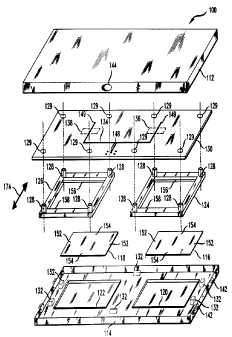
FIG. 3 illustrates patch antenna assembly 100. The assembly is enclosed
by conductive rear housing section 112 and non-conductive front housing
section 114.
to Resonator elements 116 and 118 are held in non-conductive frames 124 and
126,
respectively. Posts 128 of the non-conductive frames are received by post
holes 129 of
feedboard 130. Feedboard 130 is positioned in front housing section 114 by
positioning
tabs 132. Feedboard 130 is multilayered and contains a ground plane, a plane
containing
conductor 134, and insulating layers on the top and bottom surfaces and
between
conductor 134 and the ground plane. Slots 136 and 138 in the ground plane
permit a
radio frequency (RF) signal on conductor 134 to couple to resonators 116 and
118 so that
RF energy may be transmitted through front housing section 114. Rear housing
section
112 then mates with front housing section 114 and locks in place by
interacting with
locking tabs 142. Rear section 112 contains opening 144 which provides a
passage
2o through which a conductor can pass for attachment to point 148 on conductor
134.
Non-conductive frames 124 and 126 include posts 128. It should be noted that
frames 124 and 126 may be manufactured using injection molding and may also be
formed as one part rather than two in order to simplify assembly. Post holes
129 in
feedboard 130 receive posts 128. The frames may be held in place by melting
the portion
of post 128 that extends through feedboard 130 to form a mushroom cap that
holds the
frames in place. Resonators 116 and 118 are snapped into frames 124 and 126,
respectively. The frames hold resonators 116 and 118 approximately 1/10 of a
wavelength at the frequency of operation away from feedboard 130. Front
housing
section 114 includes tabs 132 that assist in the alignment or placement of
feedboard 130
CA 02322735 2000-10-10
Egmond-Guinn- Papatheodorou-Roberts-Tsai-Zimmerman 1-4-2-1-3-10
4
into front housing section 114. If the frames and resonators are placed into
front housing
section 114 before they are attached to feedboard 130, ridges 120 and 122
assist in the
alignment or placement of the frames and resonators. It should be noted that
guide ridges
120 and 122 do not extend higher than non-conductive frames 124 and 126 to
ensure that
ridges 120 and 122 do not interfere with the 1/10 wavelength spacing provided
by the
non-conductive frames.
FIG. 4 illustrates a cross section of antenna assembly 100. Interlocking tabs
142
and 170 hold front housing sections 114 and 112 together. Resonators 116 and
118 are
supported in frames 124 and 128, respectively. Retention tabs 180 hold the
resonators in
t o their respective frames. As mentioned earlier, the frames may be attached
to feedboard
130 using posts 128; however, it is also possible to maintain the relationship
between the
frames and feedboard using a compression force provided by rib 172 of rear
housing
section 112. The placement of the frames in front housing section 114 is
facilitated by
guide ridges 120 and 122. Placement of feedboard 130 is facilitated by
placement tabs
132. Rear housing section 112 includes a series of parallel ribs 172. When
sections 114
and 112 are interlocked using tabs 170 and 142, ribs 172 press down on the
components
beneath them so that the components are effectively compressed between ribs
172 and the
inner surface of front housing section 114.
In reference to FIG. 3, it should be noted that the radio frequency (RF)
signal on
2o conductor 134 couples to the resonators through sections 149 of conductor
134 which
pass over slots 136 and 138. The desired dominant polarization direction 174
is shown.
When the RF signal couples to the resonators, the higher current densities on
the
resonators occur on the sides of the resonators that are parallel to conductor
sections 149.
As a result, side sections 152 of resonators 116 and 118 contain the higher
current
densities. In order to limit interfering with the higher current densities, it
is desirable that
frames 124 and 126 minimize contact with the resonators along side sections
152. In
order to minimize this contact, frames 124 and 126 make contact with the
resonators
along perimeter surfaces 154 using retention tabs and support surfaces or
ridges
positioned along frame sides 156 and 158.
CA 02322735 2000-10-10
Egmond-Guinn- Papatheodorou-Roberts-Tsai-Zimmerman 1-4-2-1-3-10
FIG. 5 illustrates frame 124. It should be noted that frames 124 and 126 are
identical and may be formed in one piece by using ribs that interconnect the
two frames.
The frames may be fabricated using a material such as a polycarbonate or
Noryl~ type
plastic. (Noryl~ is a registered trademark of General Electric Company.) In
general, the
5 material should have a low dielectric loss tangent. Frame surface 190 faces
in the
direction of the inner surface of front housing section 114 when the patch
antenna
assembly is constructed. Posts 128 are received in holes 129 of feedboard 130.
It should
be noted that posts 128 may be inserted through the receiving holes of
feedboard 130 and
then heated to create a mushroom-type cap that will hold the frame in place.
It is
1 o desirable that frame sides 192 do not contact the resonator because the
higher current
densities on the resonator occur along surfaces adjacent to these edges and
contacting the
high current density surfaces will interfere with the resulting radiation
pattern. In
general, the frame should not contact the resonator along edges that are
parallel to the
conductor that couples the RF signal to the resonator or along surfaces that
are adjacent to
those edges. Sides 156 of frame 124 include retention tabs 180 and support
surface 194.
The resonator is inserted into the frame by pressing the resonator past
retention tabs 180
so that the edges of the resonator are supported by surface 194 and are held
against or
adjacent to surface 194 by tabs 180.
FIG. 6 is a cross section of the frame of FIG. 5 along line A-A. The figure
2o illustrates posts 128, retention tabs 180 and resonator support surfaces
194.
FIG. 7 is a cross section of the frame of FIG. 5 along line B-B. Posts 128 are
illustrated along with tabs 180 and support surface 194: