Note: Descriptions are shown in the official language in which they were submitted.
CA 02322737 2000-10-10
Franey-Guinn-Manzione-Tsai 17-5-18-5
PATCH ANTENNA USING NON-CONDUCTIVE
THERMO FORM FRAME
Cross Reference To Related Inventions
This application is related to the following commonly assigned an concurrently
filed US Patent Applications entitled "Patch Antenna", Serial No. 09/425358;
and "Patch
Antenna Using Non-Conductive Frame, Serial No. 09/425374.
1 o Background of the Invention
1. Field of the Invention
The present invention relates to antennas; more particularly, patch antennas.
~ 5 2. Description of the Prior Art
FIG. 1 illustrates an exploded view of a prior art patch antenna assembly. Non-
conductive front housing 10 and conductive rear housing 12 form the outer
surfaces of
the antenna assembly. The two sections of the housing enclose multi-layered
feedboard
14, resonators 16 and 18 and spacers 20. Spacers 20 are attached to front side
22 of
2o feedboard 14 by screws 24. Screws 24 mate with threads on the inside of
spacers 20 by
passing through holes 26 in feedboard 14. Resonators 16 and 18 are attached to
spacers
20 in a similar fashion. Screws 28 mate with threads on the inside of spacers
20 by
passing through holes 30 in resonators 16 and 18. The spacers are chosen so
that they
provide a space of approximately 1/10 of a wavelength at the frequency of
operation
25 between feedboard 14 and resonators 16 and 18. The assembled feedboard,
spacers and
resonators are mounted inside of the enclosure formed by front housing 10 and
rear
housing 12. A signal to be transmitted by the antenna assembly is provided to
conductor
40 of mufti-layered feedboard 14. Conductor 40 is typically positioned on one
layer of
CA 02322737 2000-10-10
' ~ Franey-Guinn-Manzione-Tsai 17-5-18-S
2
feedboard 14 such as on top layer 42. An insulating layer is typically
provided between
conductor 40 and a ground plane layer of feedboard 14. The ground plane layer
22
normally has openings or slots 44 which allow the signal from conductor 40 to
couple to
resonators 16 and 18 so that the signal can be transmitted through front
housing 10.
FIG. 2 provides a more detailed illustration of the assembled feedboard 14,
spacers 20
and resonators 16 and 18. Screws 24 pass through holes in feedboard 14 to mate
with the
threaded inside portion of spacer 20. Similarly, screws 28 pass through holes
in
resonators 16 and 18 to mate with the threaded inside portion of spacers 20.
This prior art patch antenna assembly suffers from several shortcomings. The
1o assembly is expensive to assemble because of the many individual parts such
as eight
spacers and 16 screws. The spacers are expensive to mass produce because they
include
threaded inner portions. Additionally, the holes made through resonators 16
and 18 to
allow screws 28 to mate with spacers 20 create unwanted patterns in the radio
frequency
energy radiated by the antenna assembly. For example, if the antenna is being
used for a
~ 5 horizontally polarized transmission, the holes introduce additional non-
horizontal
polarizations in the transmitted signal.
Summary of the Invention
The present invention solves the aforementioned problems by providing a non-
2o conductive frame that supports the resonators. The frame supports the
resonators without
making holes in the resonators and thereby avoids the problem of creating
unwanted
electric field polarizations. Additionally, the frame grasps the resonators in
areas of low
current density and thereby avoids creating additional disturbances in the
radiation
pattern. In one embodiment of the invention, the frame includes a perimeter
lip that
25 snaps over the edges of the feedboard and thereby attaches the frame to the
feedboard
without using additional components such as screws.
CA 02322737 2000-10-10
Franey-Guinn-Manzione-Tsai 17-5-18-5
3
Brief Description of the Drawing
FIG. 1 illustrates a prior art patch antenna assembly;
FIG. 2 illustrates a prior art feedboard, spacer and resonator assembly;
FIG. 3 illustrates an exploded view of a patch antenna assembly having non-
conductive frames;
FIG. 4 illustrates a cross section of an assembled patch antenna system having
non-conductive frames;
FIG. 5 illustrates a resonator receptacle with a resonator inserted; and
FIG. 6 illustrates a resonator receptacle without a resonator inserted.
to
Detailed Description of the Invention
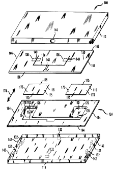
FIG. 3 illustrates patch antenna assembly 100. The assembly is enclosed
by conductive rear housing section 112 and non-conductive front housing
section 114.
Resonator elements 116 and 118 are held in non-conductive frame 124. Feedboard
is
t 5 positioned in front housing section 114 by positioning tabs 132. Feedboard
130 is
multilayered and contains a ground plane, a plane containing conductor 134,
and
insulating layers on the top and bottom surfaces and between conductor 134 and
the
ground plane. Slots 136 and 138 in the ground plane permit a radio frequency
(RF)
signal on conductor 134 to couple to resonators 116 and 118 so that RF energy
may be
20 transmitted through front housing section 114. Rear housing section 112
mates with front
housing section 114 and locks in place by interacting with locking tabs 142.
Rear section
112 contains opening 144 which provides a passage through which a conductor
can pass
for attachment to point 148 on conductor 134.
Non-conductive frame 124 is a thermo-formed using a non-conductive material
25 such as Lexan~ 101 plastic which is available from General Electric Company
(LEXAN~ is a registered trademark of General Electric Company). It should be
noted
that frame 124 may be manufactured as two parts rather than one part, or if
there are more
than two resonators, a separate frame may be used for each resonator.
Resonators 116
CA 02322737 2000-10-10
Franey-Guinn-Manzione-Tsai 17-5-18-5
4
and 118 are snapped into resonator receptacles 160 and 162, respectively, of
frame 124.
Perimeter lip 164 of frame 124 snaps over edges 166 of feedboard 130. It
should be
noted that frame 124 may have perimeter lip along two opposite edges rather
than all four
edges. This configuration is particularly useful when a separate frame is used
for each
resonator. The frame holds resonators 116 and 118 approximately 1/10 of a
wavelength
at the frequency of operation away from feedboard 130. Frame 124 also includes
channel
167 that is positioned over conductor 134 and attachment point 148. Channel
167 is
approximately 2 mm deep and it reduces any stray capacitance or inductance
that the
frame may introduce to conductor 134. Front housing section 114 includes tabs
132 that
i o assist in the alignment or placement of the assembly comprising feedboard
130, frame
124 and resonators 116 and 118 into front housing section 114.
FIG. 4 illustrates a cross section of antenna assembly 100. Interlocking tabs
142
and 170 hold front housing sections 114 and 112 together. Resonators 116 and
118 are
supported in resonator receptacles 160 and 162 of frame 124, respectively.
Retention
~ s tabs 180 hold the resonators in their respective receptacles. As mentioned
earlier, the
frame may be attached to feedboard 130 by snapping frame perimeter lip 164
over
feedboard edges 166; however, it is also possible to maintain the relationship
between the
frame and feedboard using a compression force provided by rib 172 of rear
housing
section 112. Placement of feedboard 130 in front housing section 114 is
facilitated by
2o placement tabs 132. Rear housing section 112 includes a series of parallel
ribs 172.
When sections 114 and 112 are interlocked using tabs 170 and 142, ribs 172
press down
on the components beneath them so that the components are effectively
compressed
between ribs 172 and the inner surface of front housing section 114.
In reference to FIG. 3, it should be noted that the radio frequency (RF)
signal on
25 conductor 134 couples to the resonators through sections 149 of conductor
134 which
pass over slots 136 and 138. The desired dominant polarization direction 174
is shown.
When the RF signal couples to the resonators, the higher current densities on
the
resonators occur on the sides of the resonators that are parallel to conductor
sections 149.
CA 02322737 2000-10-10
' Franey-Guinn-Manzione-Tsai 17-5-18-5
As a result, side sections 173 of resonators 116 and 118 contain the higher
current
densities. In order to limit interfering with the higher current densities, it
is desirable that
resonator receptacles 160 and 162 minimize contact with the resonators along
side
sections 173. In order to minimize this contact, resonator receptacles 160 and
162 make
5 contact with the resonators along lower current density perimeter surfaces
175 using
retention tabs and support surfaces or ridges positioned along resonator
receptacles sides
176 and 178.
FIG. 5 illustrates resonator receptacle 160 with resonator 116 snapped into
position. Retention tabs 180 hold resonator 116 in place. It should be noted
that
retention tabs 180 make contact with resonator 116 along perimeter surfaces
175 where
the current densities are lower.
FIG. 6 illustrates resonator receptacle 160 without resonator 116 inserted.
Inner
surface 188 of resonator receptacle 160 is shaped such that center portion 190
is higher
than side portions 192 and 194. This results in center section 190 providing
tension to
hold the edges of resonator 116 against lower surfaces 196 of retention tabs
180. It
should be noted that by making side sections 192 lower than raised center
section 190,
contact with high current density sections 173 of resonator 116 is minimized
when the
resonator is snapped into resonator receptacle 160.