Note: Descriptions are shown in the official language in which they were submitted.
CA 02323025 2000-10-06 _-.
Bishop 36-189-4-1 1
NON-VOLATILE MEMS MICRO-RELAYS USING MAGNETIC
ACTUATORS
Field Of The Invention
The present invention relates to Micro Electro-Mechanical Systems (MEMS),
and more particularly to the magnetic actuation of a MEMS micro-relay using
latchable magnetic materials.
Description Of The Related Art
Magnetic forces can be used to induce mechanical motion ("actuation") of
magnetic materials. Electric current flowing through a conductor (e.g. a wire)
induces a magnetic field around the conductor due to Faraday's law of
induction (e.g.
an electromagnet), and this mechanism is used to induce mechanical motion in
many
applications. Some implementation examples of electromagnetic actuation
includes
mechanical relays, bells used for fire alarm systems, and magnetic levitation
trains.
Mechanical relays generally consist of a mobile mechanical electrode that is
pulled into contact with a stationary electrode via magnetic force. In the
most general
implementation, a magnetic material is attached to the mobile electrode, and
an
electromagnet is positioned opposite the magnetic material on a stationary
electrode or
other stationary surface. Actuation of the electromagnet creates a magnetic
field
gradient that reacts with the magnetic field of the magnetic material attached
to the
mobile electrode and thereby causes the mobile electrode to be pulled or
pushed (i.e.
attracted or repelled) toward or away from the stationary electrode in a
normally-open
or normally-closed switch state of the relay, respectively.
Similar magnetic switching mechanisms have been used to actuate MEMS
relays. In these applications, current flowing through an actuation coil pulls
the
mobile micro-machined electrode toward a stationary electrode. Although such
an
actuation mechanism can deliver large actuation forces, the current required
to
maintain the switch in the on-state requires undesirable dissipation of a
large amount
CA 02323025 2000-10-06 = -
Bishop 36-189-4-1 2
of power (e.g. hundreds of milliwatts) in the control circuit of the relay.
Such high
power dissipation limits the integration of MEMS relays into CMOS circuitry
where
the amount of power thus dissipated results in an operation bottleneck, and
also
prevents high-density integration of such relays.
The operation of relays with low power dissipation becomes important as the
relay density increases. In MEMS-based relays, in particular, power
dissipation is an
important issue since the power handling capability of the substrates is
limited. Prior
art thermal actuators dissipate too much power (typically a few hundred
milliwatts)
because the induced temperature change must be maintained in order to secure
the
switch state. Similarly, prior art magnetic actuators utilizing magnetic
fields from a
current source also dissipate a large amount of power (typically a few hundred
milliwatts) in that the applied magnetic field must be maintained in order to
secure the
switch state. In applications where non-volatile switching is necessary, there
is
currently no solution to this power dissipation problem for MEMS micro-relay
implementation.
Electrostatic actuators use an applied voltage across a parallel-plate
capacitor
to induce an attractive force between the two plates and, as such, do not need
to
dissipate as much power as thermal and magnetic actuators to maintain a
switched
state, although the actuation voltage must be maintained. Since there is no
current
flow through a pair of capacitor plates, this actuation mechanism does not
dissipate
any power to maintain the actuation status (i.e. the switched status in a MEMS
relay).
There are, however, two drawbacks in this actuation scheme. The first is that
although no power need be dissipated to maintain the switched status, the
potential
difference between the two capacitor plates must be maintained. Thus, a power
failure causes the actuation status to be lost. The second drawback is that
the force
that can be provided by the electrostatic actuator is limited to a few micro
Newtons,
thereby limiting the application of such an actuator.
CA 02323025 2002-11-29
i
Summary Of The Invention
Soft magnetic materials typically exhibit continuously increasing magnetic
induction (magnetization) as the magnitude of the applied magnetic field is
increased.
Conversely, they lose most of their magnetization when tl~e applied field is
removed.
However, there are special types of magnetic materials which are easy to
magnetize
with relatively low magnetic fields as in the case of soft magnetic materials,
but retain
their magnetization with the removal of the external magnetic field as in the
case of
permanent (or hard) magnetic materiaks. Square-loop latchable magnetic
material
with a low coercive force displays properties that enable changing of the
direction of
magnetization (i.e. polarization) in the material by applying a small external
magnetic
field thereto. The value (or direction) of magnetization (i.e. polarization)
of the
latchable magnetic material remains constant even upon removal of the external
magnetic field that is used to orange its direction (See articles b~y ,S. Jin,
et al.., in
High Frequency Properties of Fe-Cr-Ta-N Soft Magnetic Materials, published in
Applied Physics Letters Vo1.70 ,.page 3161. 1997 and High-Remanance Square-
Loop
Fe-Ni and Fe-Mn MaXnetic Allv~s, in IEI~E Ti-ansaction.s cn Magnetics, Vol.
MAG-
16, page 1062, 1980. The latching nature of the material magnetization
provides an
ideal mechanism for magnetic actuation, where the direction of the
magnetization can
be selectively reversed by operation of an electromagnet, without requiring
additional
power to maintain the magnetization direction (polarization) once it has been
changed.
In accordance with a preferred embodiment of the present invention, the
actuation
device includes a mobile electrode having a first electrit;al contact and a
stationary
electrode having a second electrical contact. A square loop iatchable magnetic
material is
disposed on one of the mobile and stationary electrodes and has a
magnetization direction
that can be changed in response to exposure to an external magnetic field. At
least one
current conductor is disposed in spaced relation to the latclrable magnetic
material such
that an external magnetic field created by passing current through said at
least one current
conductor is capable of causing the magnetization direction of the latchable
magnetic
CA 02323025 2002-11-29
4
material to change to the opposite (or reverse) polarity. Unce the
magnetization direction has
been reversed, the current applied through the at last one conductor may be
discontinued. A
second magnetic material is disposed opposite the latchable magnetic material
and on the
same plane as the second electrical contact. The second magnetic material is
then selectively
S attracted to or repelled from the latchable magnetic material in response to
the magnetization
direction of the latchable magnetic material. In this manner, the first and
second electrical
contacts may be selectively connected and disconnected by changing the
magnetization
direction of the latchable magnetic n-iaterial using the external magnetic
field created by the at
least one conductor.
Other objects and features of the present invention will become apparent from
the
following detailed description considered in conjunction with the accompanying
drawings. It
is to be understood, however, that the drawings are designed solely for
purposes of
illustration and not as a definition of the limits of the invention, far which
reference should be
made to the appended claims.
In accordance with one aspect of the present invention there is provided an
actuation
apparatus for a device including a mobile electrode having a first electrical
contact and a
stationary electrode having a second electrical contact, said actuation device
comprising: a
latchable magnetic material disposed on one of the mobile and stationary
electrodes and
having a magnetization direction that is changeable in response to exposure to
an external
magnetic field; at least one electrical conductor disposed in predeterminately
spaced relation
to said latchable magnetic material such that an external magnetic field
created by passing
electrical current through said at least one conductor exposes the latchable
magnetic material
to the created magnetic field to cause a change in the magnetization direction
of said
latchable magnetic material, said changed magnetization direction being
maintained in the
latchable magnetic material after the exposure to the created external
magnetic field is
discontinued; and a second magnetic material disposed on the other of the
mobile and
stationary electrodes and in predeterminately spaced relatiar~ to said
latchable magnetic
material so that said second magnetic material is one of attracted to and
repelled from said
latchable magnetic material in response to and as a function of the
magnetization direction of
said latchable magnetic material; wherein the first and second electrical
contacts may be
selectively connected and disconnected by displacing the mobile electrode
relative to the
CA 02323025 2002-11-29
4a
stationary electrode by selectively applying electrical current to said at
least one conductor so
as to create the external magnetic field to which the iatchable magnetic
material is exposed
and thereby change the magnetization direction of said latchabie magnetic.
material using the
external magnetic field of the at least one conductor.
Other objects and features of the present invention will become apparent from
the
following detailed description considered in conjunction with the accompanying
drawings. It
is to be understood, however, that the drawings are designed solely for
purposes of
illustration and not as a definition of the limits of the invention, for which
reference should be
made to the appended claims. 1t should be further understood that the drawings
are not
necessarily drawn to scale and that, unless otherwise indicated, they are
merely intended to
conceptually illustrate the structures and procedures described herein.
Brief Description Of The Drawings
In the drawings wherein like reference numerals denote similar elements
throughout
the views:
Figure la is a schematic view of current carrying conductors according to an
embodiment of the present invention:
CA 02323025 2000-10-06 ___
Bishop 36-189-4-1 5
Figure 1b is a cross-sectional view of the current carrying conductors of
Figure
1b;
Figure 2 is a graphical representation of the magnetization of square-loop
latchable
magnetic materials as a function of an applied magnetic field;
Figure 3 is a schematic diagram of a magnetically actuated MEMS micro-relay in
accordance with an embodiment of the present invention;
Figure 4 is a schematic diagram of a magnetically actuated MEMS micro-relay in
accordance with another embodiment of the present invention; and
Figure 5 is a schematic diagram of a magnetically actuated MEMS micro-relay in
accordance with yet another embodiment of the present invention.
Detailed Description Of The Presently Preferred Embodiments
The actuation mechanism according to the present invention provides suitable
means to achieve both attractive and repulsive forces in a MEMS device while
substantially eliminating the need for power dissipation to maintain the
switched state.
The direction of actuation force (i.e. attractive vs. repulsive) can be easily
reversed by
changing the direction of current flow through a set of control conductors. In
principle, the control current need only to be supplied over a time duration
in which
the direction of magnetization (i.e. polarization) of the magnetic material is
being
reversed and latched, and the need for power dissipation is therefore
eliminated when
the actuation status is simply being maintained. Some exemplary applications
for
such mechanical actuation with low to no power dissipation include, without
limitation, mechanical relays and reflecting light switches.
While an electrically-generated magnetic field is usually produced by using
solenoid windings, such a solenoid configuration is bulky and difficult to
manufacture
in small and flat-geometry devices. For micro-devices such as MEMS, a thin and
compact design of field-generating components is essential. The present
invention
CA 02323025 2000-10-06 -
Bishop 36-189-4-1 6
thus utilizes a novel concept of thin-film processed, parallel conductor
assembly in
which the magnetic field generated by individual conductors is locally
combined or
cancelled out so as to produce an overall, in-plane, linear magnetic field
suitable for
actuation of latchable magnetic materials incorporated in the inventive device
structures. Figures la and 1b depict an embodiment of one switchable
configuration
of a set of current carrying conductors 10 for use in providing the magnetic
field H
needed to change the direction of magnetization in the soft magnetic material.
In this
embodiment each conductor 10 can have a width ranging from about 0.1 pm to 10
mm, and a thickness ranging from about 0.1 mm to 100 p.m. The conductor
material
may be selected from well-known, high conductivity metals and alloys such as
based
on Cu, Al, Au, Ag, Pt, Rh, Pd, Ru, or from superconducting materials such as Y-
Ba-
Cu-O and other materials. The number of conductors 10 that form a set can,
range
from 1 to 106, generally to cover the size of the device that is being
actuated. When
the number of conductors is greater than one, the gap between adjacent
conductors
may range from about 0.1 p,m to 1 mm to achieve the proper magnetic field
distribution for actuation. The flow direction of current I through each of
the
conductors at any given time is the same, so as to induce a quasi-uniform
magnetic
field in the vicinity of the set of conductors.
When a current I is passed through the set of conductors in the direction of
the
arrow shown by way of example in Figure la, the surface current density K can
be
calculated from the net current I that is delivered through each individual
conductor
as:
K = n1,
where h is the number of conductors per unit length. At a height h above the
conductors (where h is much smaller than the lateral width of the conductors),
the
magnetic field induced by the flowing current is parallel to the plane of
current flow
and perpendicular to the direction of flow as shown in Figure 1b. The
magnitude of
the magnetic field H is given by
CA 02323025 2000-10-06 _.,
Bishop 36-189-4-1 7
H = ,uoKl2,
where ,uo is the magnetic permeability of a vacuum. This field strength is
independent
of the height h as long as h is very small compared to the lateral width of
the
conductors. For example, if the cross-section of each current-carrying
conductor is
1 p,m x 1 p,m and the separation between adjacent conductors is 1 p.m, n =
O.S/p.m and
H is about 3.14 Oersteds per mA of current in each wire. The magnetic flux
density
B depicted in Figure 1b can be derived from the magnetic field intensity H
through
the vector relation B = ,uH, where ,u is the permeability constant of the
magnetic
medium.
Figure 2 graphically depicts the magnetization (magnetic intensity) M of a
square-loop, latchable magnetic material as a function of applied magnetic
field H.
The magnetization of the material saturates at MS, ranging from about 0.1 to
10000
gauss, when the external magnetic field exceeds a critical field strength H~.
ranging
from about 0.1 to 10000 Oersteds, also known as the coercive field of the
material.
Even when the external field is removed, the magnetization remains near MS. As
the
direction of the external magnetic field H reverses and the magnitude reaches
the
coercive field strength -H~, the direction of magnetization changes and the
magnetization saturates at MS. Upon removal of the external magnetic field,
the
magnetization remains at -MS. Again, as the direction of the external magnetic
field
reverses and the magnitude reaches the coercive field strength H~, the
direction of
magnetization reverts back to +MS. The coercive field strength H~ and the
saturated
magnetization Mf of the magnetic material can be selectively engineered by
tailoring
the material and geometry of the magnetic thin film. The coercive field should
be
within the range that the current carrying conductors can provide, and the
saturated
magnetization should be sufficiently large to supply enough magnetic force for
actuation.
With such latchable magnetic thin film placed atop of the current carrying
conductors, the orientation of the external magnetic field seen by the thin
film
CA 02323025 2000-10-06 -
Bishop 36-189-4-1 8
magnetic material due to the current flowing in the conductors can readily be
reversed
by changing the direction of current flow. When this structure (comprising the
current carrying conductors and the thin-film soft magnetic material) is
placed in
proximity to another magnetic material, the magnetic force between the two
magnetic
materials can be switched from attractive to repulsive as a function of the
magnetization direction (i.e. polarization) of the thin film magnetic
material, and this
force can be used to actuate small mechanical structures, including MEMS
devices.
The coercive force (H~), or the switching field, of the latchable magnetic
films
in the inventive devices should be within a desirable range. Too a high
coercive
would make it very difficult to switch with desirably low values of applied
current,
and too low a coercive force poses a danger of inadvertent magnetic switching
and
MEMS actuation by stray magnetic fields. The desired H~ value is in the range
of 2
- 200 Oe, and preferably 5 - 50 Oe. High magnetic saturation in the latchable
magnetic material is desirable, typically in the range of 1000 - 24000 gauss,
and
preferably 4000 - 24000 gauss. High squareness of the M-H loop of the
latchable
magnetic material is essential for efficient operation of the inventive
latchable MEMS.
The desired squareness, in terms of the ratio of remanent magnetization to
saturation
(Mr/Ms), is desirably at least 0.8, preferably at least 0.9, and even more
preferably at
least 0.95.
The latchable magnetic material is preferably in a thin film form directly
deposited onto the MEMS structure. However, the use of non-thin-film approach
is
not excluded, e.g., attaching the magnetic material using micro-printing
technology or
using pre-made and pre-sized, very thin magnetic sheet material in combination
with
adhesive carrier ribbons. The deposition of magnetic thin films can be
accomplished
by physical vapor deposition such as sputtering, evaporation, by chemical
vapor
deposition, or by electrochemical deposition such as electroplating or
electroless
deposition. The latchable magnetic films can be selected from Fe-Ta-N, Fe-Cr-
Ta-
N, Fe-Zr-N, Co-Fe, Ni-Fe , Fe-Cr-Co, and many other Fe, Co, or Ni base
ferromagnetic films. The desired high-squareless loop and latchable
characteristics
CA 02323025 2000-10-06 --
Bishop 36-189-4-1 9
can be imparted to the thin film magnetic materials by introducing magnetic
anisopropy, e.g., by using oblique incidence deposition, magnetic field
deposition,
addition of exchange anisotropy, or by post-deposition heat treatment in a
magnetic
field. The desired thickness of the latchable magnetic film in the inventive
MEMS
structure is typically in the range of 0.1 - 200 micrometers, and preferably 1
- 50
micrometers. The shape of the magnetic film can be square, rectangular, oval,
or any
irregular configuration.
The two magnetic materials on the opposing sides of the MEMS relay
structure can be both latchable. Alternative inventive designs include the
case of one
of two magnetic materials being soft magnetic (non-latchable), or permanent
magnetic (non-switchable with the maximum switching field available in the
MEMS
device), as long as the opposing side of the relay comprises the latchable
magnetic
layer. The latchable, non-volatile characteristics of the relay operation
remains the
same although the specifics of magnetic actuation may have to be altered for
optimal
performance. Non-latchable, soft magnetic thin film material may be selected
from a
number of materials with low coercive force (e.g., < 5 Oe) and low M-H loop
squareness ratio (e.g., < 0.5) such as Ni-Fe based alloys (well known as
Permalloys),
Co-Fe based alloys, Si-Fe alloys, amorphous magnetic alloys based on Fe, Ni or
Co.
Permanent magnet thin film materials may be selected from various alloys with
high
coercive force (e.g., > 100 Oe) such as based on Sm-Co, Nd-Fe-B, Fe-AI-Ni-Co
(known as Alnico), Fe-Cr-Co, Co-Fe-V (Vicalloy), Cu-Ni-Fe (Cunife).
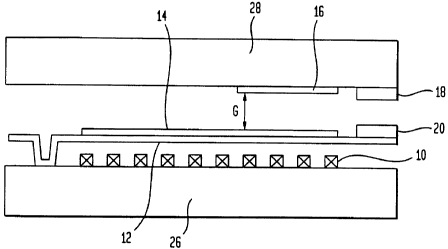
Figures 3, 4 and 5 depict alternative embodiments of implementations of the
inventive actuation mechanism in a MEMS micro-relay. As is known in the art,
the
MEMS micro-relay structure is formed by a mobile mechanical cantilever 12
having a
thickness ranging from about 0.05 to 100 microns, lengths ranging from about 1
to
10000 microns, widths ranging from 0.1 to 10000 microns, and a mobile metallic
electrode 20 carried at the free end and having a size ranging from about 0.1
to 5000
microns on a side. Actuation of the mechanical cantilever 12 causes the same
to
move up and down as desired. When cantilever 12 moves up, the mobile metallic
CA 02323025 2000-10-06 - -
Bishop 36-189-4-1 10
electrode 20 makes electrical contact with one or more fixed metallic contacts
18
having a size ranging from about 0.1 to 5000 microns generally conforming to
that of
the mobile electrode 20, to thereby establish an electrical connection
therebetween.
The electrical connection is broken when the mechanical cantilever 12 is
displaced or
moves down to create a size gap or spacing ranging from about 0.05 to 200
microns
between the metallic electrodes 18 and 20. The contact geometry may be
rearranged
to suit the particular application so that, for example, the mobile metallic
electrode 20
lies on the lower side of cantilever 12, and the fixed metallic electrode 18
lies on
substrate 26 beneath cantilever 12 (Figure 5). In that modification,
cantilever 12
must when actuated be displaced downward to establish the connection, and
upward to
break it; in either case, the actuation mechanism should enable the mechanical
cantilever 12 to move both up and down.
In the embodiment of Figure 3, the current carrying conductors 10 are
fabricated for location beneath mechanical cantilever 12, and may be disposed
or
carried directly on substrate 26. The latchable magnetic material 14 is
carried atop
cantilever 12 together with a mobile electrode or contact 20. The second
magnetic
material 16 of a high coercive field is placed above the latchable magnetic
material 14
and is adhered to another substrate 28 or other stationary surface using, for
example,
flip-chip bonding. One of ordinary skill will nevertheless recognize that
other
suitable known bonding techniques may also be utilized without departing from
the
spirit and scope of the invention. The gap G between the two magnetic
materials 14,
16 can range from about 0.05 to 500 microns. Thus, as the magnetization
direction
of the soft magnetic material 14 atop cantilever 12 is switched by changing
the flow
direction of current I in the underlying conductors 10, the two magnetic
materials
exert either mutually attractive or repulsive forces, resulting in the
respective upward
or downward displacement and motion of mechanical cantilever 12. The upward
motion of cantilever 12 causes mobile electrode 20 to contact fixed electrode
18 and
thereby actuate a switched state of the MEMS device. Corresponding downward
motion of cantilever 12 effects disconnection electrodes 20 and 18 from each
other.
CA 02323025 2000-10-06 - -
Bishop 36-189-4-1 11
Figure 4 depicts an alternative embodiment of the invention in which the
current carrying conductors 10 and the soft magnetic thin-film material 24 are
placed
on the same substrate as the fixed electrode 18, and the second magnetic
material 22
with a high coercive field is located on the mechanical cantilever 12. The
actuation
mechanism is nevertheless identical to that of the embodiment shown in Figure
3,
despite the different relative locations of the two magnetic materials 22 and
24.
Figure 5 depicts another alternative implementation of the actuating
mechanism of the invention in which the flip-chip bonded substrate is
eliminated by
rearranging the electrodes and magnetic films. In this more compact design,
the
mobile electrode 20 is placed on the lower surface of the mechanical
cantilever 12 and
the soft-latchable magnetic material 34 is arranged on an upper surface of
cantilever
12. The fixed electrode 18, second magnetic material 32 and conductors 10 are
all
carried on the surface of substrate 26 beneath mechanical cantilever 12. The
actuation
mechanism is in any event the same as that described in the embodiment of
Figure 3,
except that it is the downward displacement or motion of cantilever 12 that
brings
electrodes 18 and 20 into physical and electrical contact.
While there have shown and described and pointed out fundamental novel
features
of the invention as applied to preferred embodiments thereof, it will be
understood that
various omissions and substitutions and changes in the form and details of the
devices
illustrated, and in their operation, may be made by those skilled in the art
without
departing from the spirit of the invention. For example, it is expressly
intended that all
combinations of those elements and/or method steps which perform substantially
the same
function in substantially the same way to achieve the same results are within
the scope of
the invention. It is the intention, therefore, to be limited only as indicated
by the scope of
the claims appended hereto.
Thus, while there have shown and described and pointed out fundamental
novel features of the invention as applied to a preferred embodiment thereof,
it will
be understood that various omissions and substitutions and changes in the form
and
details of the devices illustrated, and in their operation, may be made by
those skilled
CA 02323025 2000-10-06
Bishop 36-189-4-1 12
in the art without departing from the spirit of the invention. For example, it
is
expressly intended that all combinations of those elements and/or method steps
which
perform substantially the same function in substantially the same way to
achieve the
same results are within the scope of the invention. Moreover, it should be
recognized
that structures and/or elements and/or method steps shown and/or described in
connection with any disclosed form or embodiment of the invention may be
incorporated in any other disclosed or described or suggested form or
embodiment as
a general matter of design choice. It is the intention, therefore, to be
limited only as
indicated by the scope of the claims appended hereto.