Note: Descriptions are shown in the official language in which they were submitted.
CA 02323682 2000-10-17
1
2
3
4
'
6 PAT~t
7
8 PULSED CATHODIC PROTECTION SYSTEM AND METHOD
9 BACKGROUND OF THE INVENTION
0 FIELD OF THE INVENTION
1 This invention relates to a system and method for
2 the cathodic protection of structures such as pipelines
3 and well casings disposed.in an electrically conducting
4 medium such as the ground:and more particularly to such
5 a system utilizing pulscd D.C. current to protect a
6 plurality of such structures in which the spacing between
7 the structures and/or different electrical properties of
8 the conducting medium surrounding the structures are not
9 amenable to the use of a'single pulsed source.
:0 DESCRIPTION OF THE PRIOR ART
~1. The use of cathodic protection to prevent corrosion
:2 is well established for the protection of inetal
:3 structures, such as well casings and pipe lines, that are
;4 buried in conductive soils. Cathodic protection is also
'S used for the protection of inner surfaces of tanks which
'6 contain corrosive solutions, as well as for the
17 protection of su.b-platforms, and other offshore metal
'.8 structures. It is well established that the cathodic
!9 protection can be accomplished either by the use of
30 sacrificial anodes electrically grounded to the structure
31 to be protected, or by the application of low voltage
32 direct current from a power source. In the latter method
CA 02323682 2000-10-17
2
I steady direct current, half or full wave rectified
2 current, and pulsed direct current have all been used.
3 It has been well established that, when a cathodic
3 protection current is appiied to a circuit including the
structure (cathode) to be. protected and its associated
5 anode, a layer of charge is formed at approximately 100
7 A. from the surface of the structure_ This layer of
3 charge is called a taffel.double layer. This layer acts
as a capacitor in series with the anode-cathode circuit.
J In the absence of a cathodic protection system the
I soil or other conductive:corrosive medium to which a
ferrous metal structure such as a steel pipeline is
exposed will cause an adverse chemical reaction in which
3 ferrous or iron inolecules pass into solution as positive
S ions by surrendering e'lectrons to the structure.
~ Hydrogen ions in the solution will accept the free
7 electrons and form a gas, e.g. Hz, adjacent to the
3 surface of the structure.: Oxygen molecules and certain
) other substances, if present in the solution, will also
J accept the electrons. This action results in a loss of
l iron in the structure with a consequent degradation of
2 structural integrity.
3 Direct current cathodic protection systems prevent
I (or in.hibit) the iron molecules from passing into
5 solution by providing an exterior source of free
i electrons to the structure. The electrons supplied by
7 the cathodic protection: systems reduce any oxygen
3 molecules and/or hydrogen;ions present at the surface of
3 the structure. The iron=molecules are inhibited from
J going into solution, becapse the hydrogen ion and oxygen
I molecule receptors for the iron molecule electrons have
2 been reduced by the cathodic protection system electrons-
CA 02323682 2000-10-17
3
] As a general rule, the greater the amount of current
2 (accumulated electrons per unit of time) that is supplied
3 by the cathodic protection system, the greater will be
4 the area of structure protected.
A typical steady state 15 volt and 15 ampere D.C.
G cathodic protection systein offers good protection but
7 provides only a limited umbrella of protection or throw
8 along the structure such as a pipeline to be protected.
9 Such steady state systems thus require a considerable
0 number of protection stations for a given length of the
I structure or pipe to be protected, Increasing the amount
2 of current supplied by increasing the voltage, will
3 inc:rease the throw. The average current must, however,
4 be limited such that an excess of hydrogen gas is not
5 generated at the point of application of the cathodic
6 protection system. An excess of hydrogen may cause
7 damage to protective coatings. Excess hydrogen will also
8 permeate the pipe wall, causing certain pipe materials to
9 crack or rupture.
0 It has been shown that a pulsed D.C. voltage source
1 having ail output of the order of 100-300 volts for 5-100
2 microseconds ("ps") with a duty cycle of the order of 10%
3 provides a much greater coverage (or throw) per station
4 e.g. one station every few miles of pipeline. Such
5 pulsed systems have been considered to be particularly
6 effective because, although the average current is still
7 in the order of magnitude of 15 amperes, the peak
S current, which is flowing for a sufficient lengtti of time
9 to cause the protective reactions to take place, will be
0 typically as high as 30.0 amperes. The pul_sed. D.C.
1 systems also cause a greater redistribution of the
2 current along the structure, such as a pipeline, because
CA 02323682 2009-04-07
4
1 of the inductive and cap~citive reactance of the anode
2 and structure system.
3 Copper-copper sulfate electrodes are conventionally
4 used to determine the effectiveness of cathodic
S protection systems in -protecting well casings and
6 pipelines. Such electrodes, comprising a copper rod
7 immersed in a copper sulfate solution (typically a gel)
8 are placed in the ground{ adjacent the well casings or
9 pipeline (e.g., 1 or 2 feet therefrom) and the potential
'0 between the metal structure an the copper rod is
1 measured. A potential, t,ypically called "the well head
2 potential", of about 1 volt is considered to provide
3 appropriate protection.
4 Prior art cathodic protection systems are disclosed
S in my prior U. S_ Patents Nos. 3,612,898; 3, 692, 650; and
6 5,324,405 (" `405 patent"),. The 1405 patent teaches an
7 improvement over the systems disclosed in the earlier
8 patents in terms of increasing the current distribution
9 or throw of the current along a pipeline or well casing
0 as well as increasing t+hQ protection of neighboring
1 pipelines or well casings. This improvement is
2 accomplished by the limit'ing current flow in the power
3 supply through the use of back emf current limiting
4 means.
5 A typical prior art; pulsed protection system is
7 illustrated in Fig. 1 of! the drawings where reference
3 numerals 10, 12 and 14 designate a D.C. voltage source,
9 an anode/cathode voltage switch and a puLse
J width/frequency control unit, respectively. The positive
output is supplied to an anode unit 16 (which may
2 comprise several discrete,metal cylindera connected in
CA 02323682 2000-10-17
I parallel) via a positive terminal 18 and the negative
2 output is supplied to a;plurality of well casings or
3 pipelines 20 and 22 via,the negative terminal 24. A
4 diode 25 (or a back emf limiter as taught in the '405
patent) is connected across the output terminals 18 and
6 24. The voltage and current waveforms V and I of the
7 output, appearing acrossthe terminals 18 and 24, are
8 shown in Figure 1 to thelright of the switch 12. As is
9 pointed out in the 1405 patent the use of diode 25
0 protects the voltage source from reverse voltage spikes
I at the expense of somewhat' limiting the current throw and
2 the protection for neighboring structures where a single
3 current source is used.
4 A problem has arisen when a single pulsed D.C.
5 source is used to protect:two or more structures from a
6 single anode unit where the spacial distances between the
7 structures andlor the electrical properties of the soil
8 or other conducting medium result in one or more
9 structures receiving excessive current while others
0 receive inadequate current for protective purposes. The
I use of a separate anode uriit and pulsed sources for each
2 neighboring well casing o:r pipeline has its own set of
3 problems as is alluded to;in the `405 patent. An under
4 protected well casing or pipeline located in adverse soil
5 conditions may need frequent replacement. The cost of
5 replacin,g a damaged well'casing or section of pipeline
7 can be very expensive. For example, the cost to replace
8 a deep well casing may =un as much or more than one
a million dollars. Thus, the problem has serious economic
0 consequences.
I There is a need for ari improved cathodic protection
2 system capable of adequately protecting muttiple
CA 02323682 2000-10-17
6
I adjacent structures such: well casings and the like
2 which are not amenable to the use of a single pulsed
3 source.
4 SOMMARY OF THE INVENTZON:
A system for the effective cathodic protection of a
6 plurality of spaced electrically conducting structures
7 such as ferrous metal pipe lines or well casings exposed
8 to an electrically conducting medium, such as the ground,
9 in accordance with the present invention comprises a
0 plurality of pulsed D.C. current sources with each source
1 being adapted to be connected to a separate structure.
2 Each current source is arranged to supply a current pulse
3 of a controllable amplitude to the associated structure
4 at a selected frequency. A control circuit is coupled to
5 each current source and: arranged to synchronize the
6 operation of the cuzrent: sources so that the current
7 pulses of all current sources occupy substantially the
8 same time frame during each cycle. In other words, each
9 of the current pulses during a cycle is initiated at
0 substantially the same time and the decay of each of the
I current pulses begins at the same time. The magnitude of
2 the current from each of the current sources may be
3 separately adjusted to provide the proper amount of
4 current to each structure,to ensure its protection. By
5 the same token, the pulse width and cycle frequency of
6 al], the current sources may be adjusted as desired.
7 It is to be noted that it is the rise or rise time
8 of the current pulses from the several pulsed D.C.
9 current sources which is controlled to occur during the
0 same time frame. The decay of the current pulses is
I dependant on the impedance of the load, i.e., the anode,
2 cathode (or well casing, pipelines etc.) and the
CA 02323682 2000-10-17
7
1 intervening conducting medium such as the soil. The term
2 curreiit rise or current rise time refers to the time
3 frame in which the current pulse is initiated until the
4 curre:nt pulse begins to !decay. Thus, the terminology
setting the pulse width of the current pulses means
6 setting the current use t,a.me for such pulses.
7 The construction and operation of the present
8 invention can best be understood by the following
9 description takeri in conlunction with the accompanying
IO drawings in which like components are designated by like
tl reference numerals.
!2 BRIEF DESCRIPTION OF THE DRAWINGS
3 Figure 1 is a blockdiagram of a state of the art
4 pulsed cathodic protection system in which current pulses
5 from a single source are applied between a single anode
6 unit and two buried structures, such as well casings;
7 Figure 2 is a block diagram of a cathodic protection
8 system for protecting a plurality of structures, such as
9 well casings or pipe liries, with the use of multiple
0 pulsed D.C. sources, in accordance with the present
1 invention;
2 Figure 3 is a block diagram of several components of
3 a pulsed current source;
4 Figure 4 is a circuit diagram, in block and
S schematic form, of a pulsed current source utilizing a
6 D.C. to D.C. converter for controlling the current
7 amplitude of the output pulse in accordance with the
3 . present invention;
Figure 5 is a schematic/block diagram of a D.C. to
) D. C. converter; and
l Figure 6 is a circuit'diagram partially in block and
scliematic form of anottier `embodiment of a pu] sed current
CA 02323682 2000-10-17
8
l source suitable for use in the invention.
2 DESCRIPTION OF THE PREFERAED EMBODIMENT
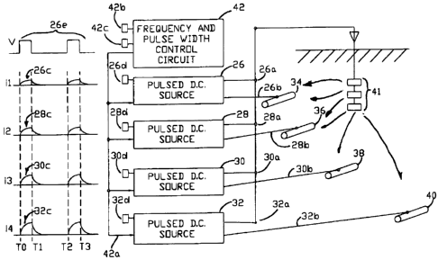
3 Referring now to Figure 2 a cathodic protection
4 system, in accordance with the present invention,
comprises a group of pulsed D.C. sources 26, 28, 30 and
6 32 with each source having a negative output terminal
7 26b, 28b, 30b and 32b arranged to be connecLed to a
8 separaL-e ferrous metal structure such as a well casing
9 (or pipe line) 34, 36, 38.and 40 as illustrated_
0 The positive output terminals 26a, 28a, 30a, and 32a
I of the D.C. sources are connected to an anode unit, as
2 shown, which is submersed in the same electrically
3 conducting medium as the well casings, e.g., the ground.
4 A frequency and pulse W~idth control circuit 42 is
5 connected to each of the pulsed D.C. sources to set the
6 width of the Yoltage and 'current pulses as well as the
7 frequency of such pulses produced across the output
8 termirials.
9 The control circuit 42 may include manually
0 controllable knobs 42b and 42c for setting the frequency
1 and pulse width of the voltage and current output pulses
2 from the pulsed sources.; The waveform of the voltage
3 across the output terminals of the D.C. source 26 is
4 shown at 26e in the diagram in the left hand portion of
5 Figure 2 with the generally square wave output voltage
6 pulses occurring during the same time frame during each
7 cycle i.e., t, to tõ tz to. t3 etc. The output voltage
8 pulses from the other pulsed D.C. sources, although not
9 shown, will also be in the form of square waves and
0 occupy the same time frame during each cycle as the
I pulses from the source 26. The current pulses (i.e.,
2 rise times) supplied by the D.C. sources to the several
CA 02323682 2000-10-17
9
1 we1l casings 34, 36, 38 and 40 and anode unit 41, which
2 occupy the same tinie frame as the voltage pulses, are
3 designated as xõ i.`, i, and i4, as illustrated. As
4 pointed out previously, the time frame (or width) of the
current pulses refers to the rise times of such pulses,
6 i. e., the time from tõ to tõ tz to t3 in the waveform
7 diagram of Figure 2.
8 As the impedance between the anode and the well
9 casings increases, due to increased distance and/or more
0 resistive soil [onditions,' greater current is required to
1 provide the necessary protection. As is illustrated in
2 the waveform diagram, by way of example, the magnitude of
3 the current pulse suppli;ed by the D.C. source 32 is
4 greater than the magnitude of the output current pulse
5 from the D.C. source 26. The amplitude or magnitude of
6 the output current pulses from .each D.C. source is
7 adjustable- The D.C- sources may include manual control
8 means such as knobs 26d, 28d, 30d, and 32d for adjusting
9 the magnitude of the output current pulses_ There are a
0 myriad of well known and conventional ways to adjust the
1 frequency, pulse width and magnitude of the output
2 current pulses fr'om the pulsed D.C. sources. If desired,
3 such parameters could be controlled by a computer.
4 Once the system of Figure 2 is installed in the
5 field, well head potential measuring electrodes are
6 typically positioned adjacent the well heads or pipelines
7 which are connected to the pulsed D.C. sources. The
8 desired pulse width and frequency of the output voltage
9 and current pulses are set by the control circuit 42-
0 The magnitudes of the output current pulses (typically
I the mean or average value of the output current) from the
;2 several D.C. sources are then adjusted until the proper
CA 02323682 2004-02-13
-10-
protection of each well casing is achieved. It should be noted that an
adjustment of the
amplitude of the output current from one dc source may and probably will
change the
current flow from one or more of the other D.C. sources to their associated
casings. Thus,
it is often necessary to make several successive adjustments of the output
current
amplitude of the several D.C. sources. It should also be noted that it may be
necessary to
reset the pulse width and frequency during the adjustment period.
Referring now to FIG. 3 the basic components of a pulsed D.C. source suitable
for use in
the system are illustrated. A D.C. voltage source 44, which may be in the form
of a
rectified (and filtered) A.C. voltage, is connected to the input of a current
amplitude
control circuit 46. The output of the amplitude control circuit is supplied to
the associated
well casing or pipeline and the anode unit via an anode/cathode voltage switch
48. The
pulse width and frequency control circuit 42 supplies a common output signal
on four
output terminals collectively identified as 42a to input circuits such as
input circuit 26e to
control the operation of the associated anode/cathode switch to set the
frequency and
width of the output pulses from all of the current sources. The amplitude of
the output
current, once set by an operator, is maintained substantially constant by
means of a
current sensing resistor unit 50 connected in a conventional feedback loop
well known to
those skilled in the art. It should be noted that the current sensing resistor
50 will
typically include appropriate filtering to provide an output voltage
thereacross which is
representative of the mean or average current.
A diode 52 is connected across the output terminals for protecting the switch
48 from
high inverse voltages. As is pointed out in the `405 patent, this diode may be
HAM_LAM 71924\1
CA 02323682 2000-10-17
I replaced with a back emf l,imiter to increase the current
2 throw at the expense of reverse voltage spikes, if
3 desired.
4 An additional breakdown of the components for use in
a pulsed D.C, source are: shown in Figure 4 wherein an
6 A.C. source supplies current to D.C. to D.C. converter 58
7 via full wave bridge rectifier 56. The output of the
8 D.C. to D.C. converter is~applied to a group of silicon
9 controlled rectifiers ("SCRs") 60, 62, 64 and 66 which
0 are controlled from a frequency control circuit 67 via a
I conventional trigger circuit 68 to form, in conjunction
2 with capacitor 70, a capacity charge/discharge circuit..
3 The capacitor 70 is connected between the anode/cathode
4 junctions of the SCRs as shown also functions to double
5 the voltage from the converter 56. SCRs 60, 66 and 62,
6 64 are triggered to conduct alternately in a conventional
7 manner, as is more fully,explained in the `405 patent.
8 The size (or value) of the capacitor 68 sets the pulse
9 width of the output pul.ses supplied to the load. In this
0 embodiment the control circuit 62 need only set the
1 frequency and synchronize th.e outputs of the severa7, D.C.
.2 pulse sources.
3 The D.C. to D.C. converter is provided with a
4 feedback voltage from a current sensing resistor unit 50
5 to maintain the current output at an adjusted setting.
.6 One type of D.C. to D.C. converter which may be
.7 employed is illustrated, in Figure 5 in which the
rectified A.C. is filtered via capaGitor 74 and applied
to the primary winding of,an isolation transformer 76 in
i0 series with the coll.ect:or-emitter circuit of a switching
power transistor such as an IGBT. The secondary winding
;2 of the transformer supplies the pulsed output current
CA 02323682 2000-10-17
12
1 through an isolation diode: 80 to an anode/cathode voltage
2 switch and to the negative output terminal. A filter
3 capacitor 82 is connected'across the output terminals as
4 shown.
The current sensing resistor unit 50, connected in
6 series with the negative output terminal (or positive, if
7 desired) supplies a feedbdck voltage via leads 84, 86 to
8 an amplitude reference circuit 88. The amplitude of the
9 reference signal in circuit 88 may be adjusted by knob 90
0 (like knob 26a of circuit 26) connected, for example, to
1 a potentiometer in a conventional manner. The output
2 signal on lead 88a from the amplitude reference circuit
3 is representative of the difference between the amplitude
4 of the reference signal and the voltage on leads 84, 86
5 which in turn is representative of the mean or average
6 amplitude of the pulsed.curzent output to the anode
7 unit/well casing. The feedback signal on lead 92 is
8 supplied to a pulse widthmodulator 94 via an isolator
9 circuit 90. The pulse width modulator, which operates at
0 a high frequency such as 20 to 200 Khz or nlore to provide
1 accurate contro], of the amplitude of the output current,
2 controls the base or gat,e electrode of the switching
3 transistor 78- It should;be noted that when used in the
4 present application it is; not necessary to include the
S isolation transformer 76 or diode 80,
6 It should be noted that if a D.C. to D.C. converter
7 is used with a non-capacitance discharge anode/cathode
S switch such as a transistor, e.g., an IGBT, then the
9 cdntrol circuit must set the pulse width as well as the
0 frequency.
1 Another example of' a pulsed D.C. source is
2 illustrated in Figure 6 Wherein an adjustable current
CA 02323682 2000-10-17
13
1 amplitude current control circuit 96 is placed on the
2 A-C. side of a pulsed D.C. source with a power switching
3 transistor 98 such as an IGBT serving as the
4 anode/cathode voltage switch. A trigger circuit 100
under the control of the frequency and pulse width
6 control circuit 42 sets the frequency and pulse width of
7 the output pulses. The current amplitude control circuit
8 96, which may utilize SGRs or Triacs in a well known
9 manner to adjustably control the portion of each half
0 cycle of the input sine: wave supplied to the bridge
i rectifier, receives a feedback signal on lead 101. The
2 feedback signal from the C,urrent sensing resistor unit 50
3 is representative of theload (anode/cathode) current.
4 The control circuit 96, in response to the feedback
5 signal maintains the value of the adjusted current output
6 to the bridge rectifier substantially constant.
7 It should be noted that while an SCR or Triac type
8 amplitude control circuit 96 wilJ. operate satisfactorily
9 to control the magnit-ude,of the current pulses to the
.0 load these circuits are inherently inefficient because of
.1 power losses in the SCRs or Triacs. In contrast, D.C, to
.2 D.C. converters are typically much more efficient due to
7 the low resistance drop through the switching transistor.
4 There has thus been described a cathodic protection
5 system and method for providing improved protection for
6 multiple structures such;as well casings or pipelines.
7 While the invention has been described in connection with
8 several embodiments, it is not intended that the scope of
9 the invention be limited to such embodiments and examples
0 discussed above. Various alternatives, modifications,
1 and equivalents will become apparent to those skilled in
2 the art without departing from the spirit and scope of
CA 02323682 2000-10-17
14
1 the invention as defined by the appended claims.
3
4
i
i
7
=
~
'
=
)
{
}
{