Note: Descriptions are shown in the official language in which they were submitted.
CA 02323982 2000-10-19
6-367
RF AMPLE HAYnVG A DUAL SLOPE PHASE MODULATOR
'this ~.ve~on relates ~o RF amplifiers and, more particularly, to an RF
amplifier having
a dual slope phase modulator for varying the phase of an RF signal.
It has been observed in an AM transmitter that the RF carnet signal may become
shifted
in phase because of variations in the Ievei of audio modulation. This may
result in distortions
particularly in digital radio broadcasting. An object is to provide RF phase
predistortion to
compensate for any phase error caused by an amplitude modulation system. This
should be
accomplished without changing the duty cycle (mark to space ratio) of the
output RF signal as
compared with the input RF signaL
io It has been known to phase shift an RF signal. One example of a phase
shifting circuit
is illustrated in Fig. l to which attention is now directed. In this version,
an RF signal made up
of a train of poises 10 is obtained from a suitable RF source 12. This RF
signal is supplied by
way of a phase shifting circuit to an RF transmitter, including a power
amplifier 20, and, thence,
to as antrem~a 22. 'i'l~e phase shifting circuit includes a potentiometer
including a resistor
portion 30 connected between ground and a B+ voltage supply source and an
adjustable wiper
arm 32 which applies a control level signal, such as V~, by way of an inductor
34 to a junction
point 36. This junction point is fed with the RF signal by way of a capacitor
40 and a resistor R1.
A tang diode CR1 is cormected between ground and the junction point 3b. The
junction
point 36 is corulecbed to the power amplifier 20 by way of a capacitor 42. The
capacitor 20 is
2o connected by a resistor 44 to ground. In this known version, the slopes of
the input RF signal 10
are modulated to create a small amount of phase shift. The modified RF output
signal is
digiitized and transformed back to a logic level. Consequently, a simulated
phase shift is
created.
The tuning diode CR1 is the heart of the circuit and its body capacitance
changes
2s proportionally to the voltage applied across it A variable low pass filter
comprised of resismr
Rl and diode CRl is created by varying t~ control signal V~. This variable low
pass filter
modifies the slope of the incoming RF signal to create a virtual phase shift
by tilting the slopes
of the rising and falling edges to obtain the RF output signal as shown at 50.
The control is
limited because the control level (VJ is fil#ered through a low pass filter
which creates group
3o delay and limited bandwidi~.
Reference is now made to Fig. 2 which illustrates another known circuit for
use in
shifting the phase of an RF signal. This circuit is similar to that of Fig. 1
and to simplify the
dOn herein similar compcmen#s are yderrtified in both figw~es with the same
character
i
CA 02323982 2000-10-19
6367
references and only the differences will be discussed below.
in Fig. 2, the phase arntrol shifting circuit includes a differential
amplifier 60 including
a pair of NPN transistors 62 and 64 having their emitters connected together
in common and,
thence, through a resistor 66 to the wiper arm 32 of the potentiometer. The
base of transistor 62
s is connected to the junction of a resistor 70 and a capacitor C1 connected
together in series
between ground and the collector of the transistor. The base of transistor 64
is connected to
ground by a resistor 76 and the collector is connected fio a V+ voltage
source. The collector of
the transistor 62 is connected to resistor Rl and by way of a capacitor 42 it
is also connect~eed fio
the input of the power amplifier 20. The capacitor 42 is connected bo ground
by way of
resistor 74. The control voltage V~ obtained from the poteentiometer is used
i3o control the current
gain of the transistors and, in turn, the current flow through the capacitor
C1. By varying the
current through capacitor C1, a variable low pass filter is created comprised
of resistor R1 and
capacitor C1. This variable low pass filter modifies the slope of the incoming
RF signal. and
cremes a ~rirhial phase shift by tilting the slopes of the rising and tailing
edges of the RF output
is signa150.
The output duty cycle (mark to space ratio) in the circuits of Figs. l and 2
is not directly
proportional to the input signal because the RF output signal is AC-coupled
and this removes
the DC information on the original RF input signal causing a level shift of
the RF output signal _,
AIso, the circuits shown in Figs.1 and 2 have very limited dynamic range of
adjustments
zo because while the slope of the signal is gradually changed, the envelop of
the signal is also
gradually changed. The acceptable range of phase modulation is on the order of
one tenth of
an RF wavelength.
The present invention includes an RF amplifier systiem having a phase
modulator for
varying the phase of an RF signal, comprising an RF source for providing an RF
signal made up
25 of a first train of pulses exhibi#ing a fined frequency and fixed duty
pulse cycle and each pulse
is of a fixed amplitude and duration, said modulator including, integrating
means for converting
each pulse cycle of said RF signal into a dual slope symmetrical ramp signal
which varies in
magnitude from a minimum level to a maximum level and then back to said
minimum level for
each pulse cycle, means for providing a first level signal and a second level
signal equally
3o spaced from a reference level characterized in that said reference level is
midway between said
minimum and maximum levels of said ramp signal, dual slope comparing means for
comparing
said dual slope ramp signal with said first and second level signals and
providing a first pulse
signal for a time duration corresponding with the time duration that said ramp
signal exceeds
2
CA 02323982 2000-10-19
6-367
said first level signal and a second pulse signal for a tune duration
corresponding with the time
duration that said second level signal exceeds said ramp signal, first and
second pulse
generators frn respectively receiving said first and second pulse signals and
providing therefrom
first arid second trigger pulses, bistable means responsive to said first and
second trigger pulses
s to be in respective first state in response to a first trigger pulse and a
second state in response
to a second trigger pulse and providing an output RF signal.made np of a
second train of pulses
of said fixed frequency and said fixed duty cycle of said first pulse train
and being shifted in
phase therefrom by an amount related to the magnitude of said first level
signal or said second
level signal
An object of the present invention is bo provide means for shifting the phase
of an RF
signal to obtain a phase shifted output signal while maintaining the duty
cycle of the RF input
signal
Conveniently, an RF source provides an RF signal made up of a first train of
pulses
exh~iting a fixed frequency and fixed duty pulse cycle and wherein each pulse
is of a fined
amplitude and duration. The modulator includes an integrator for converting
each pulse cycle
of the RF signal into a dual slope symmetrical ramp signal which varies in
magnitude from a
minimum level bo a naaaannum level and then back fio fine nvninaum level for
each pulse cycle.
A first level signal and a second level signal are provided and are equally
spaced from a
rLevel which is midway between the minimum and maximum levels of the ramp
signal.
20 A dual slope comparator compares the ramp signal with the first and second
level signals and
provides a first pulse signal for a time duration corresponding with the time
duration that the
ramp signal vcceeds the first level signal and a second pulse signal for a
time duration
corresponding with the time duration that the second level signal exceeds the
ramp signal. First
and second pulse generators respectively receive the first and second pulse
signals and provide
2s first and second trigger pulses. A bistable circuit responds fio the first
and second trigger pulses
to be in respective first and a second states and provides an output RF signal
made up of a
second train of pulses shif6ed in phase from the first train by an amount
related fio the
magnitude of the first level signal or the second Level signal.
The ~vention also includes a method of varying the phase of an RF signal that
is made
3o up of a first train of pulses exhibiting a iced frequency and fvced duty
pulse cycle and wherein
each pulse is of a fixed amplitude and duration, said method including the
sfieps of:
integrating the RF signal by converting each pulse cycle of said RF signal
into a dual
slope spmnnetrical ramp signal which varies in ~nagniixide from a minimum
level to a rnaxmnum
CA 02323982 2000-10-19
6367
level and then back bo the minimum level for each pulse cycle, characterized
by providing a
control level signal having a magnitude representing the desired phase shift
of said RF signal
and developing from said control level signal a first level signal and a
second level signal that
are equally spaced from a reference level which is midway between the minimum
and
s maximum levels of the Iamp signal;
comparing the first and second level signals with a ramp signal and providing
a first
pulse signal for a time duration corresponding with the time duration that the
ramp signal
exceeds the first level signal and a second pulse signal for a time duration
corresponding with
the time duration that the second level signal exceeds the ramp signal;
IQ providing first and second trigger pulses in response to the respective
first and second
pulse signals; and, operating a bistable circuit in response to the first and
second trigger pulses
so that said bistable circuit is in resperkive first and sernnd states in
response to said first and
second trigger pulses and providing an RF signal dependent on the operation of
said bistable
ci~uitso that the output RF signal is made up of a second train of pulses of
said fixed frequency
and said fixed duty cycle of said first pulse train and being shifted in phase
therefrom by an
amount relafied to the magnitude of said control level signal.
The invention will now be described, by way of example, with reference to the
accompanying drawings, wherein:
Fig. 2 is a prior art schematic-block diagram illustration of an RF amplifier
system
2o employing phase shifting circuitry;
Fig. 2 is another prior art schematic block diagram of an RF amplifying system
employing Phase shifting drcuitry;
Pig. 3 is a schematic-block diagram illustration of one embodiment of the
present
invention;
25 Fig. 4 is a graphical illustration including a plurality of wavefarms
illustrating the
operation of the invention herein;
Fig. 5 is a graphical illustration similar to that of Fig. 4 but showing
additional aspects
of the operation herein; and,
Fig. 6 is a schemafic-block diagram illuslzation of a second embodiment of the
present
3o imvent~n.
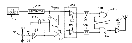
Reference is now made to Fig. 3 which illustrates a first embodiment of the
invention.
In this embodiment, various components are similar to those in Figs.1 and 2
and consequently
like character references will be employed with only the differences being
described in detail.
4
CA 02323982 2000-10-19
6.36
The lZF input signal is obtained from an RF source and this signal is made up
of an input train
of pulses exhibiting a fined frequency and a fixed duty pulse cycle and each
pulse is of a fixed
amplitude and duration. This RF input signal is supplied to the dual slope
modulator 100
constructed in accordance with the present invention. This modulator includes
a linear
integrator 102, a dual slope comparator 104, a pair of pulse generators 106
and 1~ and an S-It
flip-$op 110 which provides the output RF signal which is then amplified by a
suitable power
amplifier 20 and transmitted by way of an antenna 22
In the embodiment illustrated, the circuit is able to provide a fixed and
dynamic phase
shift up to one-half of an RF wavelength (a./ 2). The output phase shift Td
(see Figs. 5 and b) is
io directly proportonal bo the input phase shift control signal V~. The input
phase control is
wideband in its operation without any low pass filtering that would limit the
frequency
response of the phase modulation requirement as in the case of the prior art
described herein
with reference to Figs. l and 2
As shown in Fig. 3, the input 13F signal, having a wave#orm 200 as shown in
Fig. 5, is
supplied to the integrator 102. This is a linear integrator that converts each
pulse cycle of the
RF signal into a dual slope symmetrical ramp signal, having a waveform 202 as
shown in Fig.
5. This ramp signal varies in magnitude from a n~nimum Level to a maximum
level and then
back to the minimum level for each pulse cycle (refer to Fig. 5).
The control level signal V~ is applied through an amplifier 112 to the
negative or
2o inverting input of an operational amplifier 114. The output from the
integrator 102 is applied
across a divider circuit including a resistor 116 and a capacitor 118 to
ground. A reference
voltage level Vo is taken at the junction of the resistor i16 and capaciiwr
118 and this voltage is
applied to the positive or non-inverting inputof the operational amplifier
114. The outputtaken
from amplifier 1I2, voltage V~, is supplied to the negative or inverting input
of an operational
amplifier serving as a voltage comparator 120 in the dual slope comparator
104. The output
voltage Vb of operational amplifier 114 is supplied to the positive input of
an operational
amplifier taking the form of a voltage comparator 222 in the dual slope
comparator 104. The
ramp voltage obtained from the integrator 102 is supplied to the positive
input of
comparator 120 and to the negative input of comparator 122. It is to be noted
that the voltage
3o V$ obtained from amplifier 232 and the volfiage Vb obtained from amplifier
114 are equally
spaced in opposite directions from the reference voltage Vo (see the waveforms
of Fig. 5). Also
the reference level voltage of Va is midway between the minimum and maximum
levels of the
ramp signal 202 (see the waveform in Fig. ~.
5
CA 02323982 2000-10-19
6-369
The dual slope comparator 104 compares the ramp voltage obtained from
integrator 102
with the first and second level signals Va and V~ and provides a first pulse
signal A and a second
pulse signal B. Pulse signal A has a time duration corresponding with the time
duration that
the ramp signal exceeds the first level signal V,. A second pulse signal B is
provided for a time
duration corresponding with the time duration that the second level signal Vb
exceeds the ramp
signal.
More specifically, it will be noted from Figs. 3 and 5 that the dual slope
comparator 104
includes three input ports and two output ports that are infierfaced between
the integrator 102,
the phase shift control and the output pulse generators 106 and 108. As shown
in Fig. 5 at
io waveform 204, the output of comparator 120 is a logic high signal A so long
as the ramp signal
is greater than the first level signal Va. Similarly, as shown in waveform 206
in Fig. 5, the output
of comparator 122 will be at a logic high signal B so long as the second level
signal Vb is greater
than the ramp signal. It will be noted that signals Va and Vb are tracked
together and are in
opp~ite directions relative fio the voltage reference Vo (see Fig. 5j. The
dual level sampling
is ensures the recreation of the duty cycle of the original signal. The
reference level Vo is zero
when the duty cycle of the RF input is 5090. The first level signal Va is
adjustable between the
peak to-peak levels of the ramp voltage (see Fig. 5j. Also, it is to be noted
that:
Vb = 2Vo - V, (Equation 1)
The pulse generators 106 and 108 are respectively triggered by the leading
edges of the
2o positive output pulses A and B taken from comparators 120 and 122
respectively. Thus each
SET pulse, such as in the waveform 208 in Fig. 5, is triggered by the leading
edge of signal A.
The SET pulse is of short duration but is of a width sit to trigger an S-R
flip-flop 110 bo
be discussed below. Similarly, the RESET pulse R obtained from poise generator
108 is
illustrated by the waveform 210 in Fig. 5.
25 A bistable circuit taking the illustrative form an S-R flip-#Iop 110
includes a pair of logic
gates 130 and 132 connected as shown and providing an output signal X, as
shown by the
waveform 214 in Fig. 5, fio the power amplifier 20 for transmitting an RF
signal by way of the
ani~enna 22 The SET and RESET ports of flip-flop 110 respectively receive
trigger pulses from
the pulse generators 106 and 108 to change from one state to the other. The
output signal X
3o corresponds in duty cycle with the original RF input signal as will be
nofied by comparing the
waveform 224 of the output signal X with the waveform 200 of the RF input
signal (see Fig. 5).
It will be noted that the output signal X is shifted by a phase delay Td. This
time or phase delay
is linearly proportional fin the phase shift control signal V~ obtained from
the potentiometer 30
CA 02323982 2000-10-19
6-369
{Fig. 3). It is to be notied that the circuit can also be used as a delay line
with the maximum delay
adjustrnent of one-half wavelength. The output duty cycle is unaffected using
this dual slope
modulator of Fig. 3.
The waveforms of Fig. 4 illustrafie the operation with delay time (Td) up to
one-fourth
s of a wavelength {~1./ 4). The sample points x1 and x2 travel on opposi~be
slopes of wavefarm 202.
Reference is now made fio the waveforms of Fig. 5 which are similar to those
of the waveforms
of Fig. 4 and like waveforms are identified with the same character
references. In Fig. 5, a larger
phase delay is produced wherein the delay time {Td) is greater than ~,/4.
Reference is now made fio the embodiment illustrated in Fig. 6. This
embodiment is
io similar to that of the embodiment of Fig. 3 and to simplify the description
herein, like
components are identified with like character references and only the
differences will be
described below. This embodiment illustrafies an audio input supplied to an
input audio
buffer 300 and then is supplied to an audio modulating circuit 302 which
provides the audio
level to the RF power amplifier 20, as well as bo a level translator 304. This
provides the control
s5 signal V~ to the amplifier 112 within the dual scope modulator 100. The
output from the
modulator 100 is applied through an amplifier 306 bo the RF power amplifier
20. The operation
of Fig, b is the same as that set forth herein below with reference fio the
embodiment of Fig. 3 and
as described relative #o the waveforais of Fig. 4 and 5.
An RF amplifier system and method for varying the phase of an RF signal made
up of
2o a first train of pulses exhibiting a fixed frequency and fixed duty pulse
cycle and wherein each
pulse is of a fixed amplitude and duration. An integrator converts each pulse
cycle of the RF
signal ~~ a dual slope symmetrical ramp signal. A first level signal and a
secand level signal
are provided and are equally spaced from a reference level The dual slope ramp
signal is
compared with the first and second level signals. A first pulse signal is
provided for a time
25 duration corresponding with the time duration that the ramp signal exceeds
the first level signal
and a second pulse signal is provided for a time duration corresponding with
the time duration
fihat the second level signal exceeds the ramp signal. First and second pulse
generators
respectively receive the first and second pulse signals and provide first and
second trigger
pulses. A bistable circuit responds to the first and second trigger pulses to
be in respective first
3fl and second sfiates and provide an output RF signal made up of a secand
train of pulses shifted
in phase from the first train by an amount related to the magnitude of the
first level signal or the
second level signal