Note: Descriptions are shown in the official language in which they were submitted.
WO 99/53740 PCT/US98/07578
ENCAPSULATION PACKAGE AND 1~THOD
OF PACKAGING AN ELECTRONIC CIRCUIT 1~ODULE
TECHNICAL FIELD OF THE INVENTION
The invention relates to the interconnection and
packaging of electronic components and, more particularly,
to a circuit module which may include a sensor and be
disposed in a harsh environment.
BACKGROUND OF THE INVENTION
As used herein, the term "circuit module" refers to an
interconnection substrate such as a printed circuit board
(PCB) having electronic components mounted thereto. A PCB
is a multi-layer substrate, having alternate layers of
insulating material and conductive material. The conductive
material of a conductive layer is patterned to have
conductive "lines" or "traces" for routing signals (and
power) from one location on the PCB to another location on
the PCB. In the case of multiple conductive layers,
typically at least one of these layers is disposed on a
surface (e. g., the "top" surface) of the PCB. Additionally,
the conductive layer on the top surface of the PCB may be
patterned to have "pads" which serve as terminals for (i)
connecting to leads of electronic components mounted to the
PCB, or (ii) making connections to external
instrumentalities such as sockets. In this manner,
electronic components which are mounted to the PCB may be
interconnected to one another via pads on the top surface of
the PCB and conductive traces of the PCB.
Examples of electronic components which may be
incorporated in a circuit module include:
(a) "active" electronic components such as integrated
circuit (IC) devices, and the like;
(b) "passive" electronic components such as resistors,
capacitors, and inductors (including transformers), and the
like;
(c) switches, relays and the like; and
(d) sensors, transducers and the like.
The electronic components incorporated in a circuit
CA 02324325 2000-09-18
WO 99/53740 PCT/US98/07578
2
module may either be "packaged" or "bare" (not packaged).
An example of a "packaged electronic component" is a
semiconductor memory device (e. g., dynamic random access
memory, or DRAM, chip) which has been mounted and
,electrically connected to a leadframe having a plurality of
elongate conductive members ("fingers") and overmolded with
plastic. Outer portions of the leadframe fingers extend
(protrude) out of the molded plastic body and can be
connected to the conductive pads on an interconnection
substrate (PCB). In this manner, a plurality of plastic-
packaged DRAM memory devices can be mounted and connected to
a PCB, thereby forming a memory module. The memory module
can be plugged into a socket which is mounted on another
interconnection substrate, such as a "motherboard" of a
computer system, with conductive pads disposed on one or
both surfaces of the memory module making electrical contact
with resilient contact members in the socket.
An example of a "bare electronic component" is a
semiconductor device which is glued (using "die attach"
adhesive) onto an interconnection substrate and electrically
connected thereto with fine wires extending between pads on
the semiconductor device and pads on the interconnection
substrate. In order to protect the electronic component and
the wires, it is known to apply a dollop of "glob-top"
epoxy, or the like, over the electronic component and the
fine wires.
A well-known technique for making such connections to
semiconductor devices is "wirebonding". An exemplary
wirebonding technique involves:
a. feeding a fine (e. g., 1 mil diameter) gold (or gold
alloy) bond wire through a capillary which is located above
a terminal (pad) of an interconnection substrate or
electronic component mounted thereto;
b. bonding (e.g., welding) an end of the bond wire to
the terminal using a combination of pressure and heat or
ultrasonic vibration;
c. withdrawing the capillary so that the bond wire
"pays out" of the capillary, thereby forming some
CA 02324325 2000-09-18
WO 99/53740 PCT/US98/07578
3
slack in the bond wire;
d. moving the interconnection substrate (or,
conversely, the capillary), so that the capillary is located
above another terminal (pad) on the electronic component or
interconnection substrate;
e. bonding an intermediate portion of the bond wire to
the other terminal; and
f. severing the bond wire, thereby resulting in a
"loop" of bond wire extending between the terminal (pad) on
the electronic component and the terminal (pad) on the
interconnection substrate.
The present invention draws upon many of the techniques
described hereinabove to effect a novel technique for
packaging electronic circuit modules and components. Prior
to proceeding with a description of the invention, certain
additional relevant aspects of electronic packaging should
be understood.
There is often a need to test or, more broadly,
exercise electronic components and circuit modules prior to
their being shipped for installation (e. g., assembly into
systems) to ensure that they~will perform to their design
specification. This would include, in the case of
electronic components and circuit modules that can and need
to be calibrated or personalized, calibrating or
personalizing the electronic components and circuit modules.
Returning to the example of a DRAM device which has
been overmolded with plastic and which has outer portions of
leadframe fingers protruding out of the molded plastic body,
the DRAM device can be tested by making "temporary"
electrical connections to portions of the leadframe fingers
which protrude from the package body, using pins, needles
and the like. An example of a pin suitable for making a
temporary electrical connection to a terminal (in this
example, the terminal being the protruding portion of the
leadframe finger) of an electronic component is a so-called
"pogo" pin, which is generally a pin having an inner part
protruding from an outer part, and a spring maintaining the
inner part biased to an extended position. Or, in the case
CA 02324325 2000-09-18
RCV.V'ON:EPA MUENCHEN O1 : 8- 3- O : 18:17 : 216765I716~ +49 89 23994465:# 8
VGI.., Vy. 1~V.nVOIW VI i.VV LIV.VVIIIV VV,VVIVV IV. VG VVV GVV IGt~O VI IV
of a memory module having a plurality cf plastic-packaged
DRAM memory devices mounted and connected to a PCB, the
entire module can be tested by plugging the module into a
test socket of a test system, the test socket making
temporary electrical connections to the PCB and "accessing"
the components rnountzd to the PCB via the conductive traces
of the PCB.
Personalizing or calibrating a packaged circuit module
similarly involves, in a broad sense, having access to
protruding terminals of the module. For example, the module
may have a non-volatile memory (NVM) component which can be
programmed by providing signals to external terminals of the
module. Or, for example, a module can be programmed via
a
personalization components such as DIP-switches which are
part of the module and accessible from external the module.
In contrast thereto, consider the case of a packaged
circuit module which in its final form does not have any
terminals protruding from its exterior or access to
personalization components from its exterior - not even power
2U connections (e.g., battery terminals). The problem is, how
to exercise the module. An example of such a packaged
circuit rnodule lacking the inherent ability of be exercised
or personalized in its final form is a transponder module
that is fully encased to isolate its electronic components
2~ from the ambient environment, save for a sensor (e.g., a
temperature sensor) that is exposed to the ambient
environment on the exterior of the packaged circuit module.
As will become evident, the present invention is
directed to a package for encapsulating c=lectronic modules
30 and components having at least two chambers (cavities).
European Patent No. EP-A-0289439 discloses a single
chamber of an enclosure which is partially filled over a
first circuit module, thereby encapsulating a "first
chamber," and leaving the unfilled remainder of the chamber
~5 as a "second chamber." A second circuit module is placed on
top of the first filling, and then the second chamber is
filled with a second filling which covers the second circuit
module. Appropriate interconnections between circuit modules
and external connectors are made by conductors embedded in
AAIiENOED SHEET: ~ ~ q
CA 02324325 2000-09-18
RCY.VOPJ:EPA MUEIvCHEN OL : 8- 3- 0 : 18:18 : 2167661716-» +49 89 23994465:# 9
V011L Vr~ ~IVII\VGIIV01 LVV LIVfVVIIIV VVIVVfVV IV. VV VVV VVV IGy~i VfIV
9A
the first and second fillings, and th~teby passing between
chambers.
U.S. Patent No. 5,239,126 (Sony, 1993) discloses a high-
frequency circuit package including a conductive substrates
and upper and lower shielding cases which define upper and
lower shielding chambers, respectively. High-frequency
circuits are mounted on the upper and lower surfaces of the
conductive substrate within the uppEr and lower chambers,
respectively. This patent, incorporated in its entirety by
reference herein, is cited as an ehample of
HMENDED SHEET,
CA 02324325 2000-09-18
RCV.VON-EPA MIIENCHEN O1 : 8- 3- U : 18:19 : 2167651716--I +49 89 23994465:~1U
VO~I~ Vr. IIV~I~VGILAI LVV LIV1VVIIIV VVIVVIVV IV. VV VVV OVV t4~0 IV/It.
an electronic par_.kage having two chambers.
A similar package with three shielded chambers is seen
?n U.S. Patent No. 5,504,659 which discloses a structure for
the shielding of electronic components from outside
electromagnetic fields. The outside housing holds a single
pri.~.tzd circuit board which separates a "polluted" space from
a "clean" space and accommodates tha components of the device
to be shielded itself. In Fig. 2, the polluted space (24)
forms one chamber, and the housir_g forms a shielding
Nart~tion which divides off a clean space 128) forming a
second chamber with through contacts for lines connecting
between ~:he chatttbers. The printed circuit board also serves
to shield the first two chambers from a third clean space
(32) on the other side of the printed circuit board in the
'_5 housing.
LT.S. Pater:t No. 5, 627, 406 (Pace, 1997) , incorporated in
its entirety by reference herein, discloses an electronic
packaging module. A hybrid circuit (31U) forms a base and
has protuberances (3305 and metallic pads (331) on its
2U surface. Semiconductor devices (340) and other components
(341) are bonded to the protuberances and pads. A metal or
ceramic frame (350) having openings for the semiconductor
devices and other components is disposed on the surface of
the base and fits aroun3 the semiconduci.or devices and other
25 components. Plugs (370) fit inside the openings in the
frame, contact Lhe back of the semiconductor devices, and are
bonded to the frame to seal the module. Although this
) packaging module ys not an encapsulation: module, it is
referenced as illustrative of a package having two (or more)
30 side-by-side cavities (or chambers) with electronic:
components disposed in each of the cavities.
~n some cases, a circuit module is intended to be
disposed in a "harsh" environment, and iL is desirable to
isolate the electronic components of the circuit module from
she environment. An example of such an application for a
circuit module is ar. RF transponder which is disposed within
a pneumatic tire of a vehicle. Attention is directed, for
example, to the PNEUMATIC TIRE HAVING IN:'EGRATED CIRCUIT
TRANSPOA1DER AND PRESSURE TRA13SDUCER described in commonly-
Ap~ENDEO SH~E~
CA 02324325 2000-09-18
RCY. VON:EPA MI.JENCHEN G1 : 8- 3- G :. 18: 19 : ~1fi766171(i-~ +49 f35
23994466:#1 i
VG~1~ V~. IIVp;~VGI:VG1 LVV LIVlVVIlIV VV(VVIyV IVW T VVV C/VV IGbG tlll~
owned U.S. Patent No. 5,218,861, incorgclrated in its entirety
by reference herein.
08JECT OF THE INVENTION
It is an object of the present invention to provide an
improved electronic module and method for packaging the
improved electronic module as defined in one or more of the
appended claims and, as such, having the capability of being
constructed to accomplish one or more :~f the follor~ing
suosidia.ry objects.
It is therefore an object of the present invention to
provide an improved technique for packaging electronic
circuit modules.
It is another object of the present invention to
AMENDED SHEEE
CA 02324325 2000-09-18
WO 99/53740 PCT/US98/07578
6
provide an improved electronic module package.
It is another object of the present invention to provide
a technique for packaging an electronic circuit module which
permits the electronic module to be encapsulated (potted),
then exercised (e. g., calibrated), then separately potting
additional electronic components disposed within the package.
SUI~ARY OF T8E INVENTION
According to the invention, a package for encapsulating
electronic components has at least two chambers (cavities).
The chambers are open at their tops so that the chambers, and
electronic components and modules disposed within the
chambers, can be at least partially filled with encapsulating
material (potting compound). The chambers are suitably
molded from a plastic material such as thermoset epoxy,
polyphenylene sulfide, Ryton TM, or the like, by an injection
molding process.
According to an aspect of the invention, a leadframe is
disposed within the package and has elongate conductive
elements (leadframe fingers) extending from a one of the
chambers into an other of the chambers. In this manner, an
electronic component or module disposed within a one of the
chambers can be interconnected with an electronic module or
component disposed within an other of the chambers.
According to an aspect of the invention, the chambers
may separately (individually) be filled with encapsulating
material. This permits, for example, an electronic module
disposed within a one of the chambers and connected to
portions of leadframe fingers within that cavity to be potted
with encapsulating material, then electrically exercised
(e. g., calibrated or personalized) by making temporary
electrical connections (e.g., with "pogo pins") from an
external instrumentality (e. g., a test apparatus) to portions
of the leadframe fingers extending into an other of the
chambers. The potted module within the one of the chambers
can thus be exercised, either with or without an electronic
component disposed in the other of the chambers. After
exercising the potted module, the other chamber and
CA 02324325 2000-09-18
WO 99/53740 PCT/US98/07578
7
electronic component disposed therein can be potted without
"disturbing" the previously-exercised, previously-potted
module.
In an embodiment of the invention, an outer one of two
chambers surrounds an inner one of two chambers. This
embodiment includes having a one chamber surrounding an
other chamber which, in turn, surrounds yet another chamber.
In another embodiment of the invention, a one chamber
is adjacent another chamber. This includes having more than
one chamber adjacent another chamber, such as two chambers
on opposite sides of an other chamber, or three chambers
adjacent the sides of a triangular chamber, or four chambers
adjacent the sides of a rectangular chamber.
According to an aspect of the invention, the sidewalls
of a one of the chambers may be higher than the sidewalls of
an other of the chambers. In this manner, the chamber
having the higher sidewalls can, for example, be fully
filled with encapsuling material while minimizing a risk of
the encapsulating material spilling over into a neighboring
chamber.
According to an aspect of the invention, a portion of
the leadframe may extend through an outer wall of the
package to the exterior of the package.
According to another aspect of the invention, openings
may be provided in an external surface (outer wall) of the
package for making connections with components which are
external to the package.
In a representative application for the package, the
electronic module and components contained (and potted)
within the package comprise an RF-transponder and a pressure
sensor, and the entire package assembly may be mounted
within a pneumatic tire.
Other objects, features and advantages of the invention
will become apparent from the description that follows.
BRIEF DESCRIPTION OF TfiE DRAWINGS
Reference will be made in detail to preferred
embodiments of the invention, examples of which are
illustrated in the accompanying drawings. The drawings are
CA 02324325 2000-09-18
WO 99/53740 PCT/US98/07578
8
intended to be illustrative, not limiting.
Certain elements in selected ones of the drawings may
be illustrated not-to-scale, for illustrative clarity.
Often, similar elements throughout the drawings may be
referred to by similar references numerals. For example,
the element 199 in a figure (or embodiment) may be similar
in many respects to the element 299 in an other figure (or
embodiment). Such a relationship, if any, between similar
elements in different figures or embodiments will become
apparent throughout the specification, including, if
applicable, in the claims and abstract.
In some cases, similar elements may be referred to with
similar numbers in a single drawing. For example, a
plurality of elements 199 may be referred to as 199a, 199b,
199c, etc.
The cross-sectional views presented herein may be in
the form of "slices", or "near-sighted" cross-sectional
views, omitting certain background lines which would
otherwise be visible in a true cross-sectional view, for
illustrative clarity.
The structure, operation, and advantages of the present
preferred embodiment of the invention will become further
apparent upon consideration of the following description
taken in conjunction with the accompanying drawings,
wherein:
Figure lA is a top plan view of an embodiment of the
encapsulation package assembly of the present invention;
Figure 18 is a side cross-sectional view of the
encapsulation package assembly of Figure 1A, taken on a line
1B-1B through Figure lA, according to the invention;
Figure 2A is a top plan view of an alternate embodiment
of the encapsulation package assembly of the present
invention;
Figure 2B is a side cross-sectional view of an
alternate embodiment of the encapsulation package assembly
shown in FIGURE 2A of the present invention;
Figure 3 is a side cross-sectional view of an alternate
CA 02324325 2000-09-18
a; : ~.~-~ v -~>3 : is:,~,j : 2m.~n ~taic-. ~mi+.m ~n aøu;~um: # 2
f.IVI VV 1 1 I V
1 1 I VLi VV 1W LV VVV i.W 1 Va,V bl L
C
embodiment of the ene:apsuiaticn package assembly of the
ores~~nt invention;
Figure 4 is a t:c~p plan view of au el.ternate emboc:iment
elf trie encapsulation c~ackag~: .sssernbly of tt:e present
invention;
Figure 4A is an exploded, side cr~sS-sectional view of
an alternate embodirnsnt of the ?rcapsvlati o:r package assembly
r,f the present in.~c~rlticm;
Figure 48 is an assembled, side cross-sectional view of
i0 the alternate ernnodiment of the encapsulation package
assembly of Figure 4A. according to the invantion.
Figure 5A is a top plan view of are enaodiment of t'.:e
encapsul3r_icn package assembly of the present invention,
sir.;ilar to the ~mbod~menc shown in Figure lA with an
1'_1 ;additional electronic corrlponent disposed in an outez charnbor
of the package;
Figure 58 is a side cross-sectional view of t':e
encapsulation pac~;age assembly of Fic3ure 5A, taken on a line
5H-53 through Figure 5A, according to the i:wention
~G Figure 6A is a too plan view of an embodiment of t'.:e
e~cap~ul.ation Package asser.bly of the present invention,
similar to the emb~di~r;ent shown in Figure 5A with an
additional electroni<.: component disposed outside of the
package and connectea to a circuit module which is within ttie
~5 package:
Figure 68 is a side cros~-sectional view of the
en::apsulation gackaga assenirJly of Figure 5A, tai:~n en a line
6E-6B througi Figure 6A. accoraing to the invention;
Figure 6C is a side view of the ~t:l_apsulation package
assFmbly of Figure 6R. taken on 4 li:.e 6C-dC, according to
r_hc. invention;
Figure 7A-7D ~ re crl;,ss-secticrnal viN~Is of a technique
for filling the chambers of the an encapsu'_aticn package
ass~_rrin ~y of the present i nver:tion. with potting compound ( s )
3': Figure 8A is a top plan view of an alternate eribodirne:W
of the encapsulation packages assembly of the present
invention;
~tE~9ED SHEEt
CA 02324325 2000-09-18
WO 99/53740 PCT/US98/07578
Figure 8B is a side cross-sectional view of the
encapsulation package assembly of Figure 8A, taken on a line
8B-8B through Figure 8A, according to the invention;
5 Figure 9A is a top plan view of an alternate embodiment
of the encapsulation package assembly of the present
invention;
Figure 98 is a side cross-sectional view of the
encapsulation package assembly of Figure 9A, taken on a line
10 9B-9B through Figure 9A, according to the invention;
Figure 9C is a top plan view of a technique for further
packaging the encapsulation package assembly of the present
invention;
Figure 9D is a side cross-sectional view of the further
packaged encapsulation package assembly of Figure 9C. taken
on a line 9D-9D through Figure 9C. according to the
invention;
Figure l0A is a side cross-sectional view of a
technique for preparing the encapsulation package assembly
of the present invention for assembly to a monitored object,
such as a pneumatic tire; and
Figure 108 is a schematic illustration of the
encapsulation package assembly of the present invention
assembled to a monitored object, such as a pneumatic tire,
according to the invention.
DETAILED DESCRIPTION OF THE INVENTION
Figures lA and 18 illustrate an embodiment an
encapsulation package assembly 100 of the present invention.
In this, and in subsequently-described embodiments, the
drawings and accompanying descriptions thereof are also
illustrative of techniques for packaging electronic modules
and components. For example, the technique illustrated in
Figures lA and 1B generally involves placing (disposingy a
circuit module 102 into a cup-like, open-ended container
(encapsulation package) 104, so that the circuit module 102
can be encapsulated with a potting compound such as "glob-
top" epoxy, and can thereby be protected from adverse
' effects of being disposed in a harsh environment-.
CA 02324325 2000-09-18
WO 99/53740 PCTNS98/07578
11
The encapsulation package 104 has a generally planar
base portion 106 which may, as illustrated, be in the
configuration of a disc, having a circular periphery. The
base portion 106 has an inner surface (floor) 106a and an
outer surface 106b. An outer sidewall 108 extends upwardly
(as best viewed in Figure 18) from the periphery of the
inner surface 106a of the base portion 106. An inner
sidewall 110 extends upwardly (as best viewed in Figure 18)
from the inner surface 106a of the base portion 106 from a
position which is within the periphery of the base portion
106.
In the case that the base portion 106 is in the
configuration of a disc, it has an overall outside diameter
of "D". The outer sidewall 108 is suitably in the form of a
cylindrical ring having a diameter "D" and a height "H".
The inner sidewall 110 is suitably in the form of a
cylindrical ring having a diameter "d" which is smaller than
the diameter "D" of the outer sidewall 108 (i.e., D>d), a
height "8 "commensurate with (approximately equal to) the
height of the outer sidewall 108 and is generally concentric
with the outer sidewall 108. In this manner, two chambers
(cavities, wells) are formed: an outer annular chamber 112
and an inner cylindrical chamber 114, the space between the
inner and outer sidewalls 110 and 108 being approximately
constant (i.e., D-d) around their respective circumferences.
Both chambers 112 and 114 have a base and sidewalls, and are
open at their tops so that they can be filled with
encapsulating material, as described in greater detail
hereinbelow.
As best viewed in Figure 1A, the inner sidewall 110 may
not be entirely cylindrical, but rather may be provided with
a flat portion 116 spanning approximately one quarter (90°)
of the circumference of the inner wall 110 in a chord-like
manner. In this case, as illustrated, the space between the
inner and outer sidewalls 110 and 108 is greater in the
region of the flat portion 116 of the inner sidewall 110.
As will be described in greater detail hereinbelow,
CA 02324325 2000-09-18
WO 99/53740 PCT/US98/07578
12
providing the inner sidewall 110 with a flat portion 116
enhances the utility of (applications for) the encapsulation
package 104.
The encapsulation package 104 is suitably formed, using
well-known techniques, from a plastic material such as
thermoset epoxy, polyphenylene sulfide, Ryton TM, or the
like, by an injection molding process, and the base portion
106, outer sidewall 108 and inner sidewall 110 may all have
the same thickness. Exemplary dimensions (expressed in
millimeters, "mm") for the encapsulation package 104 are as
follows:
(a) the diameter "D" of the base portion 106 (and of
the outer sidewall 108) is in the range of from 25.0 mm to
50.0 mm, such as 32.0 mm;
(b) the diameter "d" of the inner sidewall 110 is in
the range of from 10.0 mm to 40.0 mm, such as 20.0 mm;
(c) the height "a" of the inner and outer sidewalls 108
and 110, respectively, is in the range of from 3.0 mm to 6.0
mm, such as 5.0 mm~ and
(d) the thickness of the base portion 106, the outer
sidewall 108 and the inner sidewall 110 is in the range of
from 1.0 mm to 2.0 mm, such as 1.5 mm.
It should clearly be understood that the encapsulation
package 104 of the present invention is not limited to the
dimensions set forth immediately hereinabove. The
encapsulation package 104 can be larger, or smaller than
described.
Nor is it essential that the outer and inner sidewalls
108 and 110, respectively, have the same heights. For
example, the outer sidewall 108 can be shorter than the
inner sidewall 210, and vice-versa.
Nor is the encapsulation package 104 of the present
invention limited to having a base portion 106 with a disc-
like configuration. The configuration of the base portion
106 can be rectangular, triangular, trapezoidal, or the
like.
Nor is it mandatory that the encapsulation package 104
of the present invention be formed of a thermoplastic
CA 02324325 2000-09-18
WO 99/53740 PCT/US98/07578
13
material. Other materials, including insulating and
conductive materials may be used. For example, the
encapsulation package 104 could readily be formed from two
punched-out metal cups, one having a smaller diameter than
the other, which are spot welded together at their base
portions. Generally, however, if the encapsulation package
were to be made from a conductive material (e.g., steel), it
would generally be preferred to dispose a layer of an
insulating material (e.g., parylene) on interior surfaces of
the encapsulation package.
Generally, the encapsulation package 104 has two
sidewalls 108 and 110 so that the outer and inner chambers
112 and 114, respectively, can separately be filled with
potting compound, or with two different potting compounds,
as described in greater detail hereinbelow.
The circuit module 102 is disposed within the inner
chamber 114 of the encapsulation package 104, and is mounted
(as best viewed in Figure 18) to the inner surface (floor)
106a of the base portion 106 in any suitable manner, such as
with an adhesive 118. A suitable adhesive 118 is epoxy.
The circuit module 102 suitably, but not necessarily,
comprises an interconnection substrate 120 such as a printed
circuit board (PCB), such as a reinforced epoxy laminate
having a thickness of twenty mils, and having a glass
transition temperature exceeding 175°C. A suitable and
preferred material for the PCB is available as "high
performance" FR-4 epoxy laminate, grade 65M90, sold by
Westinghouse Electric Corporation, Copper Laminates
Division, 12840 Bradley Avenue, Sylmar, CA 91342.
As best viewed in Figures lA. an electronic component
122 is disposed on (mounted to) the front (top, as viewed in
Figure 1B) surface of the PCB 120. For purposes of this
discussion, the electronic component 122 is a pressure
sensor, and it is desired that the electronic component 120
not be covered by potting compound filling the inner chamber
114. To this end, a cylindrical "dam" 124 (e. g., a plastic
cylinder) is disposed about the electronic component 122,
CA 02324325 2000-09-18
WO 99/53740 PCTNS98/07578
14
oriented with its axis normal to the surface of the PCB 120
(and normal to inner surface 106a of the base portion 106 of
the encapsulation package 104), and extending upward (as
viewed in Figure 1B) to a position which is approximately
coplanar with the top (as viewed in Figure 1B) edge of the
inner sidewall 110.
The electronic component 122 is connected in any
suitable manner to the PCB 120. As is known, PCBs typically
are provided with one or more layers of conductive traces,
at least one of which is on a surface thereof, fox routing
signals between various electronic components mounted to the
PCB, and are often provided with conductive pads (terminals)
to which connections to other (external) electronic
components and/or systems can be effected. In this case,
the PCB 120 is shown as being provided with a plurality
(eight of many shown) of pads 126. For purposes of
illustrative clarity, conductive traces on the surface of
the PCB are omitted, and only one other (i.e., other than
the electronic component 122) electronic component 128 is
shown mounted to the PCB 120. One having ordinary skill in
the art to which this invention most nearly pertains will
appreciate that additional electronic components (not shown)
can be mounted to the PCB 120 and interconnected with one
another to form various electronic circuits having various
functions and purposes.
Figures lA aad 1B illustrate a leadframe component,
generally designated by the reference numeral "130"),
disposed within the encapsulation package 104 on the inner
surface 106a of the base portion 106, and having a plurality
(eight of many shown) of elongate leadframe "fingers"
(conductive ribbon-like elements) 130a..130h. Each leadframe
finger 130 (a..h) has two opposite ends, either (or both) of
which may (or may not) be broader (wider) than a central
portion of the leadframe finger 130. An outer end of a
leadframe finger 130 is within the outer chamber 114, an
inner end of a leadframe finger 130 is within the inner
chamber 112, and the leadframe fingers 130 thus extend from
within the outer chamber 112, through the inner sidewall
CA 02324325 2000-09-18
WO 99/53740 PCTNS98/07578
110, to within the inner chamber 114.
It is within the scope of the invention that the
leadframe has any of a variety of patterns of conductors,
5 not only in the form of elongate "fingers". It is preferred
that none of the conductive paths of the leadframe cross-
over one another. If complex interconnections requiring
cross-overs are needed, a multi-layer interconnection
substrate could be substituted for the leadframe component.
10 As best viewed in Figure 18, the leadframe is suitably
molded into the encapsulation package 104, preferably
directly on the inner surface (floor) 106a of the bottom
portion 106. Generally, in the process of molding the
encapsulation package 109, individual leadframe fingers
15 130a..130h could be held in position with respect to one
another (i.e., stabilized) by a thin (e. g., 0.005 inch)
layer or film (not shown) of insulating material such as
Kapton. Alternatively, the leadframe fingers 130a..130h are
held in position with respect to one another by additional
portions (not shown) of the leadframe which can be excised
after molding.
It should be understood that in this embodiment, and in
other embodiments described hereinbelow (for example, as
shown in Figures 4A and 9A), that portions (e. g., leadframe
fingers) of the leadframe component (130) may extend through
the outer sidewall (108) of the package 104 to permit the
leadframe to be held (clamped) in place while a mold (not
shown) is clamped down around the leadframe component for
molding the package (104).
As best viewed in Figure 18, the pads 126 of the PCB
120 are suitably electrically connected to respective ones
of the inner ends of the leadframe fingers (only the
leadframe fingers 130b and 130f are visible in Figure 18) by
any suitable means, such as with bond wires 132, using
conventional wirebonding equipment to effect a
thermocompressive wedge or ball bond between the bond wires
132 and the leadframe fingers and PCB pads. Suitable
material for the bond wires 132 includes gold and alloys
thereof in the form of a wire having a diameter of from 0.7
CA 02324325 2000-09-18
WO 99/53740 PCT/US98/07578
16
mils to 3.0 mils.
In an illustrative application for the present
invention, the circuit module 102 is a RF-transponder, the
electronic component 122 is a pressure sensor component, the
electronic component 128 is an integrated circuit, and the
encapsulation package 104 (with transponder and pressure
sensor) is mounted within a pneumatic tire to provide tire
pressure information to an external reader/interrogator or
to a driver of a vehicle riding on the tire.
In certain applications, such as the circuit module 102
being an RF-transponder having a pressure sensor 122, and
the encapsulation package 102 being mounted within a
pneumatic tire, it is desirable both to (i) encapsulate the
circuit module 102 to protect at least a portion of its
components from harsh ambient conditions (e. g., moisture,
dirt, etc), and (ii) to calibrate or personalize the circuit
module 102 prior to mounting it within the pneumatic tire.
The inventors have constructed prototype RF
transponders, such as that described hereinabove, and have
discovered that even though the pressure sensor 122 is
shielded (by the dam 124) from direct contact with the
encapsulant (potting compound), as the encapsulant cures it
can exert undesirable stresses on the pressure sensor 122,
thereby throwing off its pre-encapsulated calibration.
It is therefore a principal object of this invention to
provide a technique for partially encapsulating a circuit
module 102, then calibrating the circuit module 102, then
completing the encapsulation of the circuit module 102. The
encapsulation of the circuit module 102 within the
encapsulation package 104 is described in greater detail,
hereinbelow.
AN ALTERNATE E~ODI~NT
An encapsulation package 104 having an inner generally-
cylindrical chamber 114 within an outer annular chamber 112
has been discussed hereinabove. It is within the scope of
this invention that the inner and outer chambers can both be
rectangular.
Figure 2A illustrates an alternate embodiment of the
CA 02324325 2000-09-18
WO 99/53740 PCT/US98/07578
17
encapsulation package assembly 200 of the present invention.
As with the previous embodiment 100, the present embodiment
200 generally involves placing a circuit module 202 (compare
202) into a cup-like, open-ended container (encapsulation
package) 204 (compare 104), so that the circuit module 202
can be encapsulated with a potting compound and protected
from the environment.
Generally, as best viewed in Figure 2A. a principal
difference between the encapsulation package 104 of the
previously-described embodiment and the encapsulation
package 204 of the present embodiment is that, in the
present embodiment the outer and inner sidewalls 208
(compare 108) and 210 (compare 110) are rectangular in plan
view, rather than circular (or approximately circular).
As best viewed in Figure 2B, another difference between
the encapsulation package 104 of the previously-described
embodiment and the encapsulation package 204 of the present
embodiment is that, in the present embodiment the dam 224
(compare 124) disposed about the electronic component 222
(compare 122) is advertently made to extend higher, by a
distance "hl" than the height " B~ " of the sidewalls 208
and 210.
As in the previously-described embodiment, in this
embodiment the encapsulation package 204 has a generally
planar base portion 206 (compare 106) which may (as best
viewed in Figure 2A) be in the configuration of a rectangle,
having an inner surface (floor) 206a (compare 106a) and an
outer surface 206b (compare 106b). An outer sidewall 208
(compare 108) extends upwardly (as best viewed in Figure 28)
from the periphery of the inner surface 206a of the base
portion 206. An inner sidewall 210 (compare 110) extends
upwardly (as best viewed in Figure 28) from the inner
surface 206a of the base portion 206 from a position which
is within the periphery of the base portion 206.
The base portion 206 is in the configuration of a
rectangle, and has a base length dimension "B" and a base
width dimension "TR". The length "B" may or may not be equal
CA 02324325 2000-09-18
WO 99/53740 PCT/US98/07578
18
to the width "W". The outer sidewall 208 is suitably in the
form of a rectangular ring having a height " 8' ". The
inner sidewall 210 is suitably in the form of a rectangular
ring having a base length dimension "b" smaller the base
length dimension "B" of the outer sidewall 208 (B>b), and a
width dimension "w" smaller than the width dimension "W" of
the outer sidewall 208 (W>w), and has a height " H' " which
is approximately equal to the height of the outer sidewall
208. In this manner, two chambers are formed: an outer
chamber 212 (compare 112) and an inner chamber 214 (compare
114).
As in the previously-described embodiment, in this
embodiment the encapsulation package 204 is suitably formed
from a thermoplastic material by a molding process, and the
base portion 206, outer sidewall 208 and inner sidewall 210
may all have the same thickness. Exemplary dimensions for
the encapsulation package 104 are as follows:
(a) the base length dimension "B" of the base portion
206 (and of the outer sidewall 208) is in the range of from
25.0 mm to 50.0 mm, such as 32.0 mm;
(b) the base length dimension "b" of the inner sidewall
210 is in the range of from 20.0 mm to 40.0 mm, such as 25.0
mm;
(c) the base width dimension "W" of the base portion
206 (and of the outer sidewall 208) is in the range of from
25.0 mm to 50.0 mm, such as 32.0 mm;
(d) the width dimension "d" of the inner sidewall 210
is in the range of from 20.0 mm to 40.0 mm, such as 25.0 mmt
(e) the height " H' " of the inner and outer sidewalls
208 and 210, respectively, is in the range of from 3.0 mm to
6.0 mm, such as 5.0 mm; and
(f) the thickness of the base portion 206, the outer
sidewall 208 and the inner sidewall 210 is in the range of
from 1.0 mm to 2.0 mm, such as 1.5 mm.
It should clearly be understood that, as in the
previously-described embodiment, the encapsulation package
204 of the present invention is not limited to the
CA 02324325 2000-09-18
WO 99/53740 PCT/US98107578
19
dimensions set forth immediately hereinabove. The
encapsulation package 204 can be larger, or smaller than
described.
Nor, as in the previously-described embodiment, is it
essential that the outer and inner sidewalls 208 and 210,
respectively, have the same heights. For example, the outer
sidewall 208 can be shorter than the inner sidewall 210, and
vice-versa.
Nor, as in the previously-described embodiment, is it
mandatory that the encapsulation package 104 of the present
invention be formed of a thermoplastic material.
Generally, the encapsulation package 204 has two
sidewalls 208 and 210 so that the outer and inner chambers
212 and 214, respectively, can separately be filled with
potting compound, or with two different potting compounds,
as described in greater detail hereinbelow.
As in the previously-described embodiment, the circuit
module 202 is disposed within the inner chamber 214 of the
encapsulation package 204, and is mounted (as best viewed in
Figure 2B) to the inner surface 206a of the base portion 206
with a suitable adhesive 218 (compare 118).
As in the previously-described embodiment, the circuit
module 202 may comprises a PCB interconnection substrate
220 (compare 120) with an electronic component 222 (compare
122) and another electronic component 228 (compare 128)
disposed on its front surface, and the electronic component
222 may be a pressure sensor surrounded by a dam 224
(compare 124) to prevent the sensor from being covered when
the inner chamber 214 is filled with potting compound.
As in the previously-described embodiment, pads 226
(compare 126) of the PCB 220 are connected with bond wires
232 (compare 132) to inner ends of a plurality of elongate
leadframe "fingers" 130a..130h (compare 130a..130h) which
extend from within the inner chamber 214, through the inner
- sidewall 210 to within the outer chamber 212.
As in the previously-described embodiment, the circuit
module 202 may be an RF-transponder, the electronic
component 222 may be a pressure sensor component, the
CA 02324325 2000-09-18
WO 99/53740 PCTNS98/07578
electronic component 228 may be an integrated circuit, and
the encapsulation package 204 may be mounted within a
pneumatic tire.
5 AN AIrTERNATE ED~ODI1~NT
Encapsulation packages (104 and 204) having inner (110,
210) and outer (108, 208) sidewalls of the same height (H,
H') have been discussed hereinabove. It is within the
scope of this invention that the inner and outer sidewalls
10 of the encapsulation package can have different heights than
one another.
Figure 3 illustrates, in cross-section, another
alternate embodiment of an encapsulation package assembly
300 (compare 100, 200) including an encapsulation package
15 304 which may be circular (compare 104) or rectangular
(compare 204). The principal difference illustrated in this
embodiment is that the inner sidewall 310 (compare 110, 210)
extends to a height which is higher, by a distance "h2" than
the height " H" " of the outer sidewall 308 (compare 108,
20 208). In other words, a feature of this embodiment is that
the sidewall 310 extends further from the inside surface
306a of the base portion 306 than the sidewall 308. In all
other respects, the encapsulation package 304 is similar to
the previously-described encapsulation packages 104 and 204,
having a generally planar base portion 306 (compare 106,
206) having an inner surface 306a (compare 106a, 206a) and
an outer surface 306b (compare 106b, 206b). The outer
sidewall 308 extends upwardly from the periphery of the
inner surface 306a of the base portion 306. The inner
sidewall 310 extends upwardly from the inner surface 306a of
the base portion 306 from a position which is within the
periphery of the base portion 306. In this manner, two
chambers are formed: an outer chamber 312 (compare 112, 212)
and an inner chamber 314 (compare 114, 214), each of which
may separately be filled with potting compound, as described
in greater detail hereinbelow.
As in the previously-described embodiments (100, 200),
a circuit module comprising a PCB interconnection substrate
CA 02324325 2000-09-18
WO 99/53740 PCT/US98/07578
21
320 (compare 120, 220) is mounted to the inner surface 306a
of the base portion 306 with a suitable adhesive 318
(compare 118, 218). The PCB interconnection substrate 320
has an electronic component (not visible, compare 122, 222)
disposed on its front surface and surrounded by a dam 324
(compare 124, 224), and has another electronic component 328
(compare 128, 228) mounted on its front surface. Conductive
pads 326 (compare 126, 226) on the PCB 320 are connected
with bond wires 332 (compare 132, 232) to inner ends of a
plurality of elongate leadframe "fingers" (compare
130a..130h, 230a..230h), only two of which 330b and 330f
are visible in this view, which extend from within the inner
chamber 314, through the inner sidewall 310 to within the
outer chamber 312.
As in the previously-described embodiments (100, 200),
the circuit module 302 may be an RF-transponder, the
electronic component 322 may be a pressure sensor component,
the electronic component 328 may be an integrated circuit,
and the encapsulation package 304 may be mounted within a
pneumatic tire.
As in the previously-described embodiments (100, 200),
in this embodiment 300 the encapsulation package 304 is
suitably formed from a thermoplastic material by a molding
process, and the base portion 306, outer sidewall 308 and
inner sidewall 310 may all have the same thickness. The
encapsulation package 304 may have dimensions comparable to
(approximately equal to) those of the previously-described
encapsulation packages 104 and 204, as follows:
(a) the height " H" " of the outer sidewall 308 is
approximately equal to either the height "H" of the outer
sidewall 108 or the height " H' " of the outer sidewall 208;
(b) the cross-dimension (e. g., diameter) of the base
portion 306 (and of the outer sidewall 308) is approximately
equal to either the dimension "D" of the outer sidewall 108
or the dimensions "B" or "~" of the outer sidewall 208;
(c) the cross-dimension (e. g., diameter) of the inner
sidewall 310 is approximately equal to either the dimension
CA 02324325 2000-09-18
WO 99/53740 PCT/US98/07578
22
"d" of the inner sidewall 110 or the dimensions "b" or "w"
of the inner sidewall 210; and
(d) the inner sidewall 310 extends a distance "h2" in
the range of from 0.2 mm to 0.6 mm, such as 0.4 mm, greater
than the height " H~~ " of the outer sidewall 308.
It should clearly be understood that, as in the
previously-described embodiments, the encapsulation package
304 is not limited to the dimensions set forth immediately
hereinabove. The encapsulation package 304 can be larger,
or smaller than described. Additionally, although the inner
sidewall 310 is shown as being higher (taller) than the
outer sidewall 308, it is within the scope of the invention
that the outer sidewall 308 would be taller than the inner
sidewall 310.
AN ALTERNATE ~ODI~1T
Encapsulation packages (104, 204, 304) having two
chambers, an outer chamber (112, 212, 312, respectively)
which surrounds an inner chamber (114, 214, 314,
respectively), have been discussed hereinabove. It is
within the scope of the invention that an encapsulation
package has two (or more) chambers which are adjacent one
another.
Figure 4 illustrates yet another embodiment of an
encapsulation package assembly 400 the present invention.
As with the previously-described embodiments 100, 200 300,
the present embodiment 400 generally involves placing a
circuit module 402 into a cup-like, open-ended container
(encapsulation package) 404, so that the circuit module 402
can be encapsulated with a potting compound and protected
from the environment.
This embodiment 400 is comparable to the embodiment 200
in that the inner chamber 414 (compare 214) is shown as
being rectangular, but it may have another shape (e. g.,
circular, trapezoidal, triangular, etc.)
This embodiment 400 differs from the previously-
described embodiments 100, 200 and 300 in that rather than
having a single outer chamber (112, 212, 312) surrounding
the inner chamber (114, 214, 314) at least one outer chamber
CA 02324325 2000-09-18
WO 99/53740 PCTNS98/07578
23
412a or 412b is shown as being disposed adjacent the inner
chamber 414. In this illustration, two outer chambers 412a
and 412b are shown as being disposed on opposite sides of
the inner chamber 414. It is within the scope of the
invention that additional outer chambers (not shown) could
be disposed on other sides of the inner chamber. For
example, a triangular inner chamber could have three outer
chambers, one outer chamber disposed adjacent each one of
the inner chamber's three sides. Or, a rectangular inner
chamber (as shown) could have four outer chambers, one outer
chamber disposed adjacent each one of the inner chamber's
four sides.
The encapsulation package 404 is similar to the
previously-described encapsulation packages 104, 204 and 304
in that is has a generally planar base portion 406 (compare
106, 206, 306) having an inner surface 406a (compare 106a,
206a, 306a) and an outer surface 406b (compare 106b, 206b,
306b). An outer sidewall 408 (compare 108, 208, 308)
extends upwardly from the periphery of the inner surface
406a of the base portion 406. A first inner sidewall 410a
extends upwardly from the inner surface 406a of the base
portion 406 from a first position which is within the
periphery of the base portion 406, and a second inner
sidewall 410b extends upwardly from the inner surface 406a
of the base portion 406 from a second position which is
within the periphery of the base portion 406. More
particularly, the outer sidewall 908 is rectangular, has
four sides 408a, 408b, 408c and 408d, and has an overall
width dimension "X" and an overall length dimension "Y"
(compare the dimensions "B" and "W").
The first inner sidewall 410a is disposed a distance
"xl" inward from a one side 408a of the outer sidewall 408,
and extends between an adjacent side 408b of the outer
sidewall 408 to another adjacent side 408d of the outer
sidewall 408 which is opposite the side 408b of the outer
sidewall 408, thereby forming the first outer chamber 412a
which has a width dimension "xl" and a length dimension "Y".
The second inner sidewall 410b is disposed a distance
CA 02324325 2000-09-18
WO 99/53740 PCT/US98/07578
24
"x2" inward from a side 908c of the outer sidewall 408 which
is opposite the side 408a of the outer sidewall 408, and
also extends between the adjacent side 408b of the outer
sidewall 408 to the other adjacent side 408d of the outer
sidewall 408 which is opposite the side 408b of the outer
sidewall 408, thereby forming the second outer chamber 412b
which has a width dimension "x2" and a length dimension "Y".
The first and second inner sidewalls 410a and 410b also
define two sides of the inner chamber 414, the other two
sides of the inner chamber 419 being defined by central
portions of the sides 408b and 408d of the outer sidewall
408, thereby forming an inner chamber 414 which has a width
dimension "x" and a length dimension "Y". Evidently, as
illustrated, the overall width dimension "X" of the outer
sidewall 408 equals the sum of the width dimensions "xl",
"x2" and "x" of the first outer chamber 412a, the second
outer chamber 412b and the inner chamber 414 respectively.
(X = xl + x2 + x)
In this manner, three chambers are formed: two outer
chambers 412a and 412b (compare 112, 212, 312) and an inner
chamber 414 (compare 114, 214 , 314), each of which may
contain an electronic component or module, and each of which
may separately be filled with potting compound.
As in the previously-described embodiments (100, 200,
300), a circuit module comprising a PCB interconnection
substrate 320 (compare 120, 220, 320) is mounted to the
inner surface 406a of the base portion 406 with a suitable
adhesive 418 (compare 118, 218, 318). The PCB
interconnection substrate 420 has an electronic component
422 (compare 122, 222) disposed on its front surface and
surrounded by a dam 424 (compare 124, 224, 324), and has
another electronic component 428 (compare 128, 228, 328)
mounted on its front surface. Conductive pads 426 (compare
126, 226, 326) on the PCB 420 are connected with bond wires
432 (compare 132, 232, 332) to inner ends of a plurality of
elongate leadframe "fingers" 408a..408h (compare 130a..130h,
230a..230h). A first portion of the leadframe fingers
CA 02324325 2000-09-18
WO 99/53740 PC'T/US98/07578
430a..430d extend from within the inner chamber 414, through
the first inner sidewall 412a, to within the first outer
chamber 412a. A second portion of the leadframe fingers
5 430e..430h extend from within the inner chamber 414, through
the second inner sidewall 412b, to within the second outer
chamber 412b.
It is within the scope of the invention that, in the
case of there being only one outer chamber adjacent the
10 inner chamber (more correctly, this would be considered to
be a "first" chamber adjacent a "second" chamber, since
there would be no "inner" or "outer" with two side-by-side
chambers), all of the leadframe fingers would extend from
within the one chamber, through the sidewall separating the
15 two side-by-side chambers, to within the second chamber.
Alternatively, some of the leadframe fingers could extend
from within one of the first or second chambers to beyond
the outer wall of the encapsulation package.
As in the previously-described embodiments (100, 200,
20 300), the circuit module 402 may be an RF-transponder, the
electronic component 422 may be a pressure sensor component,
the electronic component 428 may be an integrated circuit,
and the encapsulation package 404 may be mounted within a
pneumatic tire.
25 As in the previously-described embodiments (100, 200,
300), in this embodiment 400 the encapsulation package 404
is suitably formed from a thermoplastic material by a
molding process, and the base portion 906, outer sidewall
408 and inner sidewalls 410a and 410b may all have the same
thickness. The encapsulation package 404 may have
dimensions comparable to (approximately equal to) those of
the previously-described encapsulation packages 104, 204 and
304, as follows:
(a) the height of the inner and outer sidewal k is
approximately equal to either the height "H" of the outer
sidewall 108 or the height " H' " of the outer sidewall 208
or the height " H" " of the outer sidewall 308;
(b) the dimensions "x" and "Y" of the inner chamber 414
CA 02324325 2000-09-18
WO 99/53740 PCT/US98/07578
26
are approximately equal to the dimension "d" of the inner
chamber 114, or the inner dimensions "b" and "w" of the
inner chamber 214, or the inner dimension " d~~ " of the
inner chamber 314: and
(c) the dimension "xl" is approximately no greater than
one-quarter the dimension "JC", the dimension "x2" is
similarly approximately no greater than one-quarter the
dimension "X", and the dimension "x1" is approximately equal
to the dimension "x2".
It should clearly be understood that, as in the
previously-described embodiments, the encapsulation package
404 is not limited to the dimensions set forth immediately
hereinabove. The encapsulation package 404, and portions
thereof, can be larger, or smaller than described.
Nor, as in the previously-described embodiment, is it
essential that the outer and inner sidewalls 408 and 410a/b,
respectively, have the same heights.
TWO (OR MORL) SEPARATE, JOINABI~E CBAb~ERS
A number of embodiments are described herein where two
or more chambers of an encapsulation package are formed as
one unitary structure. It is within the scope of this
invention that two (or more) chambers of an encapsulation
package can separately be formed, then joined together to
form a single encapsulation package.
Figure 4A illustrates an encapsulation package assembly
450 (compare, e.g., 400) having two separate chambers 452
(compare, e.g., 412b) and 454 (compare, e.g., 419). Each
chamber 452 and 454 has a base portion 456 and 458,
respectively (compare, e.g., 406). For purposes of this
description, the base portions 456 and 458 are square.
The chamber 452 has a sidewall 460 extending upwardly
(as viewed) from a periphery of its base portion 456. Two of
four portions of the sidewall are visible in this figure,
which is a "slice"-type cross-sectional view, and are
labeled 460a and 460b. As will become evident, when the two
chambers 452 and 454 are joined with one another, the
sidewall portion 460a will perform the function of an
CA 02324325 2000-09-18
WO 99/53740 PCT/US98/07578
27
"outer" sidewall portion, and the sidewall portion 460b will
perform the function of 'an "inner" sidewall portion.
In a similar manner, the chamber 454 has a sidewall 462
extending upwardly (as viewed) from a periphery of its base
portion 458. Two of four portions of the sidewall are
visible in this figure, and are labeled 462a and 462b. As
will become evident, when the two chambers 452 and 454 are
joined with one another, the sidewall portion 462a will
perform the function of an "outer" sidewall portion, and the
sidewall portion 462b will perform the function of an
"inner" sidewall portion.
Figure 4A illustrates a representative one of what may
be a plurality of elongate members 464 protruding from the
inner sidewall portion 462b of the chamber 454 in a
direction (towards the left, as viewed in the figure) of the
chamber 452, and is shown as being formed with a barb or
pawl at its distal end. The elongate member 464 is
preferably formed integrally with (e. g., molded together
with) the chamber 454. An opening (hole) 466 is formed in
the inner sidewall portion 460b of the chamber 452 at a
location corresponding to the location of the elongate
member 464. In this manner, when the two chambers 452 and
454 are joined with one another, the elongate member 464
will protrude though the opening 466, thereby securing the
two chambers 452 and 454 together, with the inner sidewall
460b of the chamber 452 being disposed intimately against
(abuts) the inner sidewall 462b of the chamber 454, as
illustrated in Figure 4B. When the chambers 452 and 454 are
joined with one another, the outer surfaces of their base
portions 456 and 458, respectively, are preferably coplanar
with one another.
Figure 4A also illustrates a representative one of what
may be a plurality of leadframe fingers 468 which have been
molded into the chamber 454 and, as mentioned hereinabove,
which extends through the outer sidewall 462b of the chamber
454. An opening (hole) 470 is formed in the inner sidewall
portion 460b of the chamber 452 at a location corresponding
to the location of the leadframe finger 468. In this
CA 02324325 2000-09-18
WO 99/53740 PCT/US98/07578
28
manner, when the two chambers 452 and 454 are joined with
one another, the leadframe finger 468 will protrude though
the opening 470, into the chamber 452, as illustrated in
Figure 4B.
It should be understood that the illustrations of
Figures 4A and 48 are shown without any modules or
components within the chambers of the encapsulation package,
for illustrative clarity. One will also notice that the
chamber 459 is illustrated as having higher (taller)
sidewalls than the chamber 452, in the manner described
hereinabove with respect to Figure 3.
After joining the two chambers 452 and 454 together, in
the manner described hereinabove, they may individually be
filled with potting compound (not shown). Evidently, if the
chamber 454 is filled to at least the level of the opening
(466), the potting compound will serve to secure the distal
end of the elongate member 464 in place, within the chamber
454, thereby substantially preventing the two chambers from
being separated from one another.
It is within the scope of the invention that an
adhesive (not shown) is disposed on one or both of the
sidewalls 460b and 462b of the chambers 452 and 454,
respectively, prior to assembling the chambers to one
another.
The elongate member 464 is shown as being integrally
formed with the chamber 454. This is generally preferred in
the case that after the two chambers 452 and 454 are
assembled to one another, the chamber 454 is filled with
encapsulation material (as described hereinbelow) prior to
the chamber 452 being filled with encapsulating material.
It is, however, within the scope of the invention that the
elongate member 464 be integrally formed with the sidewall
960b of the chamber 452, and the opening 466 be formed in
the sidewall 462b of the chamber 454.
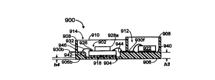
ADDING A COI~ONENT IN TSE OUTER CgAMBER
As mentioned hereinabove, the circuit module (102, 202,
302, 902) may be a RF-transponder. Such a device typically
requires an antenna to communicate with an external reader,
CA 02324325 2000-09-18
WO 99/53740 PCT/US98/07578
29
examples of which are described in greater detail
hereinbelow.
Figures 5A arid 5B illustrate, in top and side views
respectively, an embodiment of an application for the
encapsulation package assembly 500 of the present invention.
In this application, an encapsulation package 504 of the type
described hereinabove with respect to the encapsulation
package assembly 100 of Figures lA and iB is described. In
this embodiment, an additional component 550 is disposed
within the outer chamber 512 (compare 112) of the
encapsulation package 504 (compare 104).
As in the previously-described embodiment (100), in this
embodiment 500 the encapsulation package 504 suitably has a
generally planar base portion 506 (compare 106) having an
inner surface 506a (compare 106a) and an outer surface 506b
(compare 106b). An outer sidewall 508 (compare 108) extends
upwardly (as best viewed in Figure 5B) from the periphery of
the inner surface 506a of the base portion 506. An inner
sidewall 510 (compare 110) extends upwardly (as best viewed
in Figure 58) from the inner surface 506a of the base portion
506 from a position which is within the periphery of the base
portion 506. In this manner, two chambers are formed: an
outer chamber 512 (compare 112) and an inner chamber 514
(compare 114) which can separately be filled with potting
compound, or with two different potting compounds, as
described in greater detail hereinbelow.
As in the previously-described embodiment, a circuit
module 502 (compare 102) is disposed within the inner chamber
514 of the encapsulation package 504, and is mounted (as best
viewed in Figure 5B) to the inner surface 506a of the base
portion 506 with a suitable adhesive 518 (compare 118).
As in the previously-described embodiment, the circuit
module 502 comprises a PCB interconnection substrate 520
(compare 120) with an electronic component 522 (compare 122)
and another electronic component 528 (compare 128) disposed
on its front surface, and the electronic component 522 may
CA 02324325 2000-09-18
WO 99/53740 PCT/US98/07578
be a pressure sensor surrounded by a dam 524 (compare 124)
to prevent the sensor from being covered when the inner
chamber 514 is filled with potting compound.
5 As in the previously-described embodiment, pads 526
(compare 126) of the PCB 520 are connected with bond wires
532 (compare 132) to inner ends of a plurality of elongate
leadframe "fingers" 530a..530h (compare 130a..130h) which
extend from within the inner chamber 519, through the inner
10 sidewall 510 to within the outer chamber 512.
As in the previously-described embodiment, the circuit
module,502 may be an RF-transponder, the electronic
component 522 may be a pressure sensor component, the
electronic component 528 maybe an integrated circuit, and
15 the encapsulation package 504 may be mounted within a
pneumatic tire.
The additional component 550 disposed within the outer
chamber 512 is suitably a coil antenna - in other words, an
antenna formed by a length of insulated (e. g., enamel-
20 coated) wire having two free ends 552 and 554 and wound into
a coil having several turns and, optionally several layers.
As best viewed in Figure SA, the two free ends 552 and 554
of the antenna wire 550 are shown as being connected to
portions of the two leadframe fingers 530e and 530f,
25 respectively, which are exposed within the outer chamber
512. These may be simple solder connections. Alternatively
(not shown), the exposed portions of the leadframe fingers
530e and 530f can be formed with notches or the like to
mechanically "capture" the free ends 552 and 554,
30 respectively, of the antenna wire.
MAKING CONNECTIONS TO AN EXTERNA1, COMPONENT
In the previously-described embodiment 500, an
electronic device which is an RF transponder having an
antenna 550 disposed within the outer chamber 512 of the
encapsulation package 504 was described. No components
external to the package were described.
Figures 6A, 6B arid 6C illustrate an application wherein
an electronic device which is an RF transponder has an
antenna component 650 (compare 550) which is external to the
CA 02324325 2000-09-18
WO 99/53740 PCT/US98/07578
31
encapsulation package.
As in the previously-described embodiment (500), in
this embodiment 600 the encapsulation package 604 suitably
has a generally planar base portion 606 (compare 506) having
an inner surface 606a (compare 506a) and an outer surface
606b (compare 506b). An outer sidewall 608 (compare 508)
extends upwardly (as best viewed in Figure 68) from the
periphery of the inner surface 606a of the base portion 606.
An inner sidewall 610 (compare 510) extends upwardly (as
best viewed in Figure 6B) from the inner surface 606a of the
base portion 606 from a position which is within the
periphery of the base portion 606. In this manner, two
chambers are formed: an outer chamber 612 (compare 512) and
an inner chamber 614 (compare 514) which can separately be
filled with potting compound, or with two different potting
compounds, as described in greater detail hereinbelow.
As in the previously-described embodiment, a circuit
module 602 (compare 502) is disposed within the inner
chamber 614 of the encapsulation package 604, and is mounted
(as best viewed in Figure 6B) to the inner surface 606a of
the base portion 606 with a suitable adhesive 618 (compare
518).
As in the previously-described embodiment, the circuit
module 602 may comprises a PCB interconnection substrate 620
(compare 520) with an electronic component 622 (compare 522)
and another electronic component 628 (compare 528) disposed
on its front surface, and the electronic component 622 may
be a pressure sensor surrounded by a dam 624 (compare 524)
to prevent the sensor from being covered when the inner
chamber 614 is filled with potting compound.
As in the previously-described embodiment, pads 626
(compare 526) of the PCB 620 are connected with bond wires
632 (compare 532) to inner ends of a plurality of elongate
leadframe "fingers" 630a..630h (compare 530a..530h) which
extend from within the inner chamber 614, through the inner
sidewall 610 to within the outer chamber 612.
Additionally, as best viewed in Figure 6A, two separate
pads (terminals) 630i and 630j are illustrated. These pads
CA 02324325 2000-09-18
WO 99/53740 PCT/US98/07578
32
6301 and 630j are suitably formed as part of the overall
leadframe. The function of these pads 6301 and 630j is
discussed in greater detail hereinbelow.
As in the previously-described embodiment, the circuit
module 602 may be an RE-transponder, the electronic
component 622 may be a pressure sensor component, the
electronic component 628 may be an integrated circuit, and
the encapsulation package 604 may be mounted within a
pneumatic tire.
The antenna component 650 is external to the package
604, and is formed as a length of wire having two free ends
652 and 654. Alteratively, the antenna component 650 may be
a dipole-type antenna, having two separate lengths of wire
(652 and 654).
As best viewed in Figure 6C. the free ends 652 and 654
of the external antenna component 650 pass through openings
656 and 658, respectively, in the outer sidewall 608 of the
package 609 so that they can be attached to the terminals
630i and 630j, respectively, within the outer chamber 612 of
the package 604.
An additional component 660 is optionally disposed
within the outer chamber 612 and is suitably an impedance
matching transformer having two primary leads 662 and 664
attached (e. g., soldered) to two of the leadframe fingers
630e and 630f, respectively, and having two secondary leads
666 and 668 attached (e. g., soldered) to the two additional
terminals 6301 and 630j, respectively.
As in the previously-described embodiment (500),
certain ones of the leadframe fingers (e. g., 630e and 630f)
and additional terminals (630i and 630j) can be formed with
notches or the like to mechanically "capture" the various
wires which are attached thereto.
TWO-STAGE POTTING PROCESS
As mentioned hereinabove, the encapsulation package
assemblies (100, 200, 300, 400, 500, 600) of the present
invention have two (or more) distinct chambers, each of
which can separately be filled with potting compound, or
with two different potting compounds.
CA 02324325 2000-09-18
WO 99/53740 PCT/US98/07578
33
Figures 7A-7D illustrate a technique 700 for filling the
chambers 712 (compare 112) and 714 (compare 114) of an
encapsulation package assembly 700 (compare 100) with potting
compound. The "model" fox describing this technique is the
encapsulation package assembly 100 of Figures lA and 1B.
Figure 7A shows an exemplary encapsulation package 704
(compare 104) having a generally planar base portion 706
(compare I06) having an inner surface (floor) 706a (compare
106a) and an outer surface 106b (compare 106b). An outer
sidewall 708 (compare 108) extends upwardly from the
periphery of the inner surface 706a of the base portion 706
and an inner sidewall 710 (compare 110) extends upwardly from
the inner surface 706a of the base portion 706 from a
position which is within the periphery of the base portion
706. In this manner, an inner chamber 714 (compare 114) is
formed within an outer chamber 712 (compare 112).
A circuit module 702 (compare 102) comprises a PCB 720
(compare 120) having a component 722 (shown in dashed lines,
compare 122) surrounded by a dam structure 724 (compare 124)
and another component 728 (compare 728) mounted on a surface
thereof. Pads 726 (compare 126) are provided on the surface
of the PCB 720. The circuit module 702 is disposed on the
inner surface 706a of the base portion 706, using a suitable
adhesive 718 (compare 118).
A leadframe is also disposed on the inner surface 706a
of the base portion 706 and comprises leadframe fingers 730b
(compare 130b) and 730f (compare 130f) extending from the
inner chamber 714, through the inner sidewall 710, to within
the outer chamber 712. Only these two, of a plurality of
leadframe fingers, are visible in this view (compare Figure
18). Selected ones of the pads 726 are connected to selected
ones of the leadframe fingers with bond wires 732 (compare
132), in the manner described hereinabove.
As shown in Figure 7B, in a first step of encapsulating
the electronic components disposed within the encapsulation
CA 02324325 2000-09-18
WO 99/53740 PCTNS98/07578
34
package 704, the inner chamber 714 is at least partially
filled with a quantity of potting compound (encapsulation
material) 715 which is sufficient to completely cover
portions of the leadframe fingers (730b and 730f) within the
inner chamber 714, the printed circuit board 720, the wires
726 and, optionally, the component 728, but not so much that
the potting compound 715 "spills" over the inner wall 710
separating the inner chamber 714 from the outer chamber 712.
In this figure, the potting compound 715 is shown as having a
"positive" meniscus (bowing up in the middle and down at the
edges). It is within the scope of this invention that a
potting compound having a "negative" meniscus (bowing down in
the middle and up at the edges) can be used to encapsulate
the circuit module 702 within the inner cavity 714.
Optionally, the dam structure 124 may be filled with a
silicone gel 725, either before or after filling the inner
cavity 714 with the potting compound.
As the potting compound 715 cures, it can shrink and
exert physical stress on the encapsulated components,
including upon the component 722 which, although not
encapsulated by the potting compound per se, is mounted to
another component (i.e., the PCB 720) Which is subject to the
stresses of encapsulant shrinkage. Although the forces
generated by the shrinkage may be small, they can adversely
affect the performance (or, in the least skew or offset the
response) of a stress-sensitive component (722) such as a
pressure sensor. Once the potting compound 715 has had
sufficient time to cure, whatever stresses are going to be
exerted by the potting compound 715 on the components
encapsulated thereby will have leveled out (i.e., become
constant and fixed), exhibiting a constant and fixed effect
on the pressure-sensitive components within the inner chamber
714.
In a next step, shown in Figure 7C, the components of
the circuit module 702 can be electrically exercised (e. g.,
calibrated), in the following manner. Temporary electrical
connections can be made from an external instrumentality (not
shown) to selected ones 730x and 730y (labeled as such
CA 02324325 2000-09-18
WO 99/53740 PCT/US98/07578
in this figure since these may not be the fingers 130b and
130f called out in Figure 7A) of the leadframe fingers with,
for example, "pogo" pins 742 and 744, respectively. In this
5 manner, the circuit module 702 can be powered up, and the
components of the encapsulated circuit module 702 can be
exercised (e. g., calibrated). It should be understood that,
although not shown in this figure, either before or after
powering up and exercising the encapsulated circuit module,
10 additional components (see, e.g., the antenna 550) can be
mounted within the outer chamber 712 and connected (via the
leadframe fingers) to the circuit module 702.
In a final encapsulation step, shown in Figure 7D, the
outer chamber 712 is at least partially filled with a
15 quantity of potting compound (encapsulation material) 713
which is sufficient to completely cover portions of the
leadframe fingers (730b and 730f) within the outer chamber
714, the printed circuit board 720, the wires 726 and,
optionally, a component 750 (compare 550) mounted within the
20 outer chamber 712, but not so much that the potting compound
713 "spills" over the inner wall 710 separating the inner
chamber 714 from the outer chamber 712. In this figure, the
potting compound 713 is shown as having a "positive"
meniscus, but may have a "negative" meniscus.
25 The potting compounds 713 and 715 may be the same as
one another, or different from one another.
ANOTBER ENBODI~NT OF AN E1~TCAPSUI~ATION PACKAGE ASSENBI~Y
Figures 8A and 8B illustrate yet another embodiment of
an encapsulation package assembly 800 the present invention
30 and is comparable to the encapsulation package assembly 400
described with respect to Figure 4 in that the encapsulation
package 804 (compare 404) has two chambers 812 and 814
(compare 412a or 412b, and 414, respectively) which are
side-by-side, rather than an outer chamber (e. g., 112, 212,
35 312) surrounding an inner chamber (e. g., 114, 214, 314).
The encapsulation package assembly 800 is shown without the
encapsulant, for illustrative clarity, it being understood
that the two chambers 812 and 814 can be filled in the
manner described hereinabove with potting compound.
CA 02324325 2000-09-18
WO 99/53740 PCT/US98/07578
3s
The encapsulation package 804 is similar to the
previously-described encapsulation packages in that it has a
generally planar base portion 806 (compare 406). The base
portion 806 has an inner surface 806a and an outer surface
806b. An outer sidewall 808 (compare 408) extends upwardly
from the periphery of the base portion 806. An inner
sidewall 810 extends upwardly from the base portion 806, and
defines and separates the two chambers 812 and 814 from one
another. The first chamber 812 has a width dimension "xl"
and a length dimension "y". The second chamber 814 has a
width dimension "x2" and a length dimension "y".
A first circuit module 802 (compare 402) is disposed in
the first chamber 814 and is shown as having two electronic
components 828a and 828b mounted to a printed circuit board
(PCB) 820 (compare I20).
A second circuit module 803 (compare 802) is disposed
in the second chamber 812 and is shown as having two
electronic components 822 and 828c mounted to a printed
circuit board (PCB) 821 (compare 820).
A first portion 830a..830d of the leadframe fingers
extend from within the second chamber 814, through the outer
sidewall 808 to the exterior of the encapsulation package
804, and a second portion 830e..830h of the leadframe
fingers extend from within the second chamber 814, through
the inner sidewall 810 to within the first chamber 812.
As in the previously-described embodiments, a first
circuit module 802 comprising a first PCB interconnection
substrate 820 is mounted within the first chamber 814, and
the PCB interconnection substrate 820 may have electronic
components 828a and 828b mounted on its front surface.
Conductive pads 826 (compare 426) on the PCB 820 are
connected with bond wires 832 (compare 432) to inner ends of
a plurality of elongate leadframe "fingers" 830a..830h
(compare 430a..430h.
In this embodiment, a second circuit module 803
comprising a second PCB interconnection substrate 821 is
mounted within the second chamber 812, and the PCB
interconnection substrate 821 may have one or more
CA 02324325 2000-09-18
WO 99/53740 PCTlUS98/0?5?8
37
electronic components 824 and 828c mounted on its front
surface. Conductive pads 827 (compare 826) on the PCB 821
are connected with bond wires 833 (compare 832) to inner
ends of a plurality of elongate leadframe "fingers"
830e..830h.
As in the previously-described embodiments, the circuit
module 802 may be an RF-transponder, the electronic
component 822 may be a pressure sensor component, the
electronic components 828a and 828b may be integrated
circuit devices, and the encapsulation package 804 may be
mounted within a pneumatic tire.
As in the previously-described embodiments, in this
embodiment the encapsulation package 804 is suitably formed
from a thermoplastic material by a molding process, and the
base portion 806, outer sidewall 808 and inner sidewall 810
may all have the same thickness. The encapsulation package
804 may have dimensions comparable to (approximately equal
to) those of the previously-described encapsulation packages
104, 204 and 304, as follows:
(a) the height of the inner and outer sidewalls 808 and
810 is approximately equal to either the height "g" of the
outer sidewall 108 or the height " H' " of the outer
sidewall 208 or the height " H" " of the outer sidewall 308;
(b) the dimensions "x2" and "Y" of the first chamber
814 are approximately equal to the dimension "d" of the
inner chamber 114, or the inner dimensions "b" and "~" of
the inner chamber 214, or the inner dimension " d" " of the
inner chamber 314; and
(c) the dimension "xl" of the second chamber 812 is
approximately one-half the dimension "x2".
It should clearly be understood that, as in the
previously-described embodiments, the encapsulation package
804 is not limited to the dimensions set forth immediately
hereinabove. The encapsulation package 809, and portions
thereof, can be larger, or smaller than described.
Nor, as in the previously-described embodiment, is it
essential that the outer and inner sidewalls 808 and 810,
CA 02324325 2000-09-18
WO 99/53740 PC'T/US98/07578
38
respectively, have the same heights.
ANOTHER ~ODIb~NT OF AN LNCAPSUI~ATION PACKAGE A88EN~LY
Figures 9A and 9B illustrate yet another embodiment of
an encapsulation package assembly 800 the present invention
and is comparable to the previously-described encapsulation
package assembly 800 in that the encapsulation package 904
(compare 804) has two side-by-side chambers 912 and 919
(compare 812 and 814). The encapsulation package assembly
900 is shown without the encapsulant, for illustrative
clarity, it being understood that the two chambers 912 and
914 can be filled in the manner described hereinabove with
potting compound.
The encapsulation package 904 is similar to the
previously-described encapsulation packages in that is has a
generally planar base portion 906 (compare 80f). The base
portion 906 has an inner surface 906a and an outer surface
906b. As best viewed in Figure 9B, and as described in
greater detail hereinbelow, the base portion 906 is thicker
in the chamber 912 than it is in the chamber 914.
An outer sidewall 908 (compare 808) extends upwardly
from the periphery of the base portion 906. An inner
sidewall 910 (compare 810) extends upwardly from the base
portion 906, and defines and separates the two chambers 912
and 914 from one another. The first chamber 912 has a width
dimension "xl" and a length dimension "Y". The second
chamber 914 has a width dimension "x2" and a length
dimension "Y". These dimensions are suitably similar to the
dimensions set forth with respect to the previously-
described embodiment of an encapsulation package assembly
800.
A first circuit module 902 (compare 802) is disposed in
the first chamber 914 and is shown as having two electronic
components 928a and 928b (compare 828a and 828b) mounted to
a printed circuit board (PCB) 920 (compare 820).
A first portion 930a..930d of the leadframe fingers
extend from within the second chamber 914, through the outer
sidewall 908 to the exterior of the encapsulation package
CA 02324325 2000-09-18
WO 99/53740 PCT/US98/07578
39
904, and a second portion 930e..930f of the leadframe
fingers extend from within the second chamber 914, through
the inner sidewall 910 to within the first chamber 912.
As in the previously-described embodiments, a first
circuit module 902 comprising a first PCB interconnection
substrate 920 is mounted within the first chamber 914, and
the PCB interconnection substrate 820 may have electronic
components 928a and 928b mounted on its front surface.
Conductive pads 926 (compare 826) on the PCB 920 are
connected with bond wires 932 (compare 832) to inner ends of
a plurality of elongate leadframe "fingers" 930a..930f.
In this embodiment, an electronic component 922
(compare circuit module 803) is disposed (mounted) in the
second chamber 912. Conductive pads 927 (compare 827) on
electronic component 922 are connected with bond wires 933
(compare 833) to inner ends of a plurality of elongate
leadframe "fingers" 930e..930f.
As in the previously-described embodiments, the circuit
module 902 may be an RF-transponder, the electronic
component 922 may be a pressure sensor component, the
electronic components 928a and 928b may be integrated
circuit devices, and the encapsulation package 904 may be
mounted within a pneumatic tire.
As in the previously-described embodiments, in this
embodiment the encapsulation package 904 is suitably formed
from a thermoplastic material by a molding process, and the
encapsulation package 904 may have dimensions, most of which
are comparable to (approximately equal to) those of the
previously-described encapsulation packages.
For example, the height of the inner and outer
sidewalls 908 and 910 may be approximately equal to either
the height "H" of the outer sidewall 108 or the height " H'
of the outer sidewall 208 or the height " H" " of the outer
sidewall 308. However, as best viewed in Figure 9B, it is
preferred that the inner sidewall 910 and those portions
908a, 908b and 908c of the outer sidewall 908 which,
together with the inner sidewall 910 bound the chamber 912
are higher than the remaining portions 908d, 908e and 908f
CA 02324325 2000-09-18
WO 99/53740 PCT/US98/07578
of the outer sidewall 908.
The dimensions "x2" and "Y" of the first chamber 914
may be approximately equal to the dimension "d" of the inner
5 chamber 114, or the inner dimensions "b" and "p" of the
inner chamber 214, or the inner dimension " d~~ " of the
inner chamber 314, such approximately as 5.1 mm.
The dimension "xl" of the second chamber 912 may be
approximately one-half the dimension "x2", such as
10 approximately 10.6 mm. The dimension "X" (X = xl + x2) is
suitably approximately 15.7 mm
It should clearly be understood that, as in the
previously-described embodiments, the encapsulation package
904 is not limited to the dimensions set forth immediately
15 hereinabove. The encapsulation package 904, and portions
thereof, can be larger, or smaller than described.
As mentioned hereinabove, the base portion 906 is
thicker in the chamber 912 than it is in the chamber 914.
More particularly, as best viewed in Figure 9B, the outer
20 surface 906b of the base portion 906 is generally planar, as
in the previously-described embodiments.
In this embodiment, the inner surface 940 of the base
portion within the chamber 912, whereupon the electronic
component 922 is mounted, is at a distance "h3" above the
25 outer surface 906b of the base portion 906. The inner
surface of the base portion within the chamber 914 has a
central area 942, whereupon the electronic module 902 is
mounted, which is at a distance "h4" above the outer surface
906b of the base portion 906. The distance "h3" is greater
30 than the distance "h4" (h3 > h4).
The inner surface of the base portion within the
chamber 914 is stepped, so that an area 944 outside of the
central area 942 is at a distance "h3" above the outer
surface 906b of the base portion 906. In this manner,
35 leadframe fingers (e. g., 930f) extending through the inner
sidewall 910 lie in a plane on the inner surface portion 944
of the chamber 914 and the inner surface 940 of the chamber
912. In a similar manner, other portions of the inner
CA 02324325 2000-09-18
WO 99/53740 PC1'/US98/07578
41
surface of the base portion within the chamber, outside of
the central area 942, can be stepped, so as to be at a
distance "h3" above the outer surface 906b of the base
portion 906. In this example, a portion 946 of the inner
surface of the base portion within the chamber 914 is
stepped, so as to be a distance "h3" above the outer surface
906b of the base portion 906. In this manner, all of the
leadframe fingers can be coplanar with one another.
As best viewed in Figure 9B, this results in the
electronic component 922 being disposed at a higher level
than the electronic module 902. Importantly, the increased
thickness of the base portion in the chamber 912 provides a
generally more rigid base for the electronic component 922
to be mounted upon. In the context of the electronic
component 922 being a pressure sensor, such as has been
described hereinabove, the benefits of the pressure sensor
being mounted to a relatively rigid base are evident.
Figures 9A and 9B also illustrate the concept,
described briefly hereinabove, that portions of the
leadframe, in this case the leadframe fingers 930a..930d,
may extend to the exterior of the package so that the
leadframe can be supported within a mold. In this example,
the other leadframe fingers 930e and 930f which do not
extend to the exterior of the package can be supported along
with the leadframe fingers 930a..930d by an underlying
insulating film (not shown), or by metallic webs or bridges
(also not shown) which form part of leadframe itself and
which may later be excised from the leadframe. One of
ordinary skill in the art to which the present invention
most nearly pertains will readily understand the need to and
numerous ways available for supporting the leadframe within
a mold. Inasmuch as the techniques for doing so may vary,
from application-to-application, there is no need to further
elaborate upon them in the description of the present
invention.
FURTHER PACKAGING OF THE ENCAPSULATION PACKAGE ASSEL~I'Y
Figur~s 9C aad 9D illustrate a technique for further
CA 02324325 2000-09-18
WO 99/53740 PCTNS98/07578
92
packaging of an exemplary encapsulation package assembly 900
of the present invention. The encapsulation package
assembly 900 is shown without the encapsulant, for
illustrative clarity, it being understood that its two
chambers (912 and 914) would be filled in the manner
described hereinabove with potting compound(s).
An additional encapsulation package 954 is in the form
of a simple cup-like structure, having a generally planar
base portion 956. The base portion 956 is suitably
circular, having a diameter "p", and has an inner surface
956a and an outer surface 956b. An annular sidewall 958
having a height "Q" extends upwardly from the periphery of
the base portion 956. In this manner, a cylindrical chamber
960 in formed. The height "Q" of the sidewall may be equal
to, greater than, or (preferably) no greater than the height
of the sidewalls of the encapsulation package 904.
The entire encapsulation package assembly 900 is
disposed in the chamber 912, as shown, with the outer
surface (906b) of the base portion (906) encapsulation
package (904) being disposed against the inner surface 956a
of the base portion'956 of the additional encapsulation
package 954. Any suitable adhesive 962, such as a drop of
cyanoacrylate ("super glue"), may be used to join the
encapsulation package assembly 900 to the additional
encapsulation package 954.
Suitable dimensions for the additional encapsulation
package 954 are:
the diameter "p" of the base portion 956 is in the
range of from 25.0 mm to 60.0 mm, such as approximately
32.0 mm;
the height "Q" of sidewall 958 is in the range of
from 3.0 mm to 8.0 mm, such as approximately 4.0 mm; and
the thickness "t" of the sidewall 958 is in the range
of from 0.3 mm to 2.0 mm, such as approximately 1.0 mm.
It should clearly be understood that, as in the
previously-described embodiments, the additional
encapsulation package 954 is not limited to the dimensions
CA 02324325 2000-09-18
WO 99/53740 PCT/US98/07578
43
set forth immediately hereinabove. The additional
encapsulation package 954, and portions thereof, can be
larger, or smaller than described, so long as the
encapsulation package assembly 900 fits in the additional
encapsulation package 954. The additional encapsulation
package 954 is suitably molded from the same materials as
the encapsulation packages (e. g., 104) described
hereinabove.
AN E30rMPLARY USE FOR THE ENCAPSULATION PACKAGE ASSE~I~IES
Figures l0A arid 108 illustrate an exemplary use for the
various embodiments of the encapsulation package assembly of
the present invention. As mentioned hereinabove, an
illustrative application for the encapsulation package
assembly of the present invention is to house a circuit
module (e.g., 102) which is a RF-transponder, wherein the
electronic component (e. g., 122) is a pressure sensor
component, and the encapsulation package (e.g., 104) is
mounted within a pneumatic tire to provide tire pressure
information to an external reader/interrogator or to a
driver of a vehicle riding on the tire.
Figure l0A shows an encapsulation package assembly 1000
which may be any of the aforementioned embodiments of an
encapsulation package assemblies (100, 200, 300, 400 , 450,
500, 600, 700, 800 or 900, including the further
encapsulated package 954). The package assembly 1000 is
shown as being "sandwiched" between two thin sheets 1002 and
1004, such as rubber sheets, which are pressed to remove air
bubbles from between the sheets and sealed around their
edges. An adhesive 1006 is disposed on the top (as viewed)
surface of the sheet 1002. In this manner, an encapsulated
transponder device within a "sandwich" patch 1010 is ready
to be mounted to an inside surface of a pneumatic tire.
Disposing a transponder device within a "sandwich" patch is
well known and does not form a part of the present invention
per se.
Figure 10B shows the sandwich patch 1010 of Figure l0A
mounting within a pneumatic tire 1012, on an inner surface
thereof. An external reader/interrogator 1020 having a wand
CA 02324325 2000-09-18
WO 99/53740 PCT/US98/07578
44
1022 comprising an antenna 1024 is suitably employed to poll
(interrogate) the transponder circuit disposed within the
pneumatic tire 1012, and display data retrieved therefrom on
a suitable readout 1026 such as a liquid crystal display
(LCD) panel. Using an external instrumentality to interact
with a transponder device is well known and does not form a
part of the present invention per se.
While the invention has been described in combination
with embodiments thereof, it is evident that many
alternatives, modifications, and variations will be apparent
to those skilled in the art in light of the foregoing
description. Accordingly, it is intended to embrace all
such alternatives, modifications and variations as fall
within the spirit and scope of the appended claims.
For example, selected ones of the various features set
forth in the various embodiments described hereinabove can
be "mixed and matched" so as to arrive at yet another
embodiment which incorporates the selected ones of the
features. For example, the higher inner sidewall (310)
feature of the encapsulation package (304) of the Figur~ 3
embodiment could be incorporated with the additional
component (550) feature of the encapsulation package 504 of
the Figure 5 embodiment.
CA 02324325 2000-09-18